30
Compound Semiconductors Electronic Transport Characterisation of HEMT Structures
Learn more about Lake Shore 8400 Series
Compound Semiconductors
Electronic Transport Characterisation of HEMT Structures B. J. Kelley, B. C. Dodrill, J. R. Lindemuth, and G. Du, Lake Shore Cryotronics, Inc., Westerville, OH; J.R. Meyer, Naval Research Lab, Washington, DC; L. Faraone, Department of Electrical and Electronic Engineering, The University of Western Australia, Nedlands, Australia
Introduction High-electron-mobility transistors (HEMTs) are not a new invention, but they are now coming to the forefront of the semiconductor industry because of their use in communication applications. Improved characterisation techniques are needed to continue the development of HEMTs and to improve production processes. This article discusses electronic transport characterisation of HEMT structures employing variable magnetic field, variable temperature Hall measurements and a mobility spectrum analysis software package. High electron mobility transistor (HEMT) devices have become increasingly important in the semiconductor industry, particularly for communications applications. This article discusses electronic transport characterisation of HEMT structures employing variable magnetic field, variable temperature Hall measurements using Lake Shore’s Hall Measurement System (HMS) and Quantitative Mobility Spectrum Analysis (QMSA) package.
Owing to their device structure, HEMTs are populated by multiple carrier species. Classical single field Hall measurements extract only the bulk mobility and carrier concentration. Variable field measurements in conjunction with QMSA techniques allow extraction of individual carrier mobilities and concentrations in the material. Thus, both the majority and minority carriers in the material can be investigated. In this article, variable temperature data are presented for a GaAs HEMT. The temperature-dependent behaviour of both the majority and minority carriers are discussed. Additionally, a brief discussion of the reliability of this technique and its dependence upon the field range over which Hall measurements are conducted are included.
HEMT Background Working independently, three researchers at Bell Laboratories were the first to demonstrate the high mobilities possible in modulation doped AlGaAs/GaAs heterojunctions in 1978. Researchers at the University of Illinois and Rockwell International fabricated devices exhibiting reasonable performance in 1980. These materials continued to receive serious research effort through the early 1980’s as superfast transistors with switching times on the order of 10 ps in digital applications, and as analog amplifiers capable of low noise operation at frequencies up to 60 GHz by 1985. These became known as high electron mobility transistors (HEMTs) or modulation doped FETs (MODFETs). The basis of HEMT materials is a lattice matched heterojunction between two compound semiconductors, a donor and an acceptor. In this discussion, we will use GaAsbased structures as our model material. Figure 1 is a schematic representation of a basic HEMT device.
Figure 1. Schematic representation of a GaAs based HEMT, including the two dimensional electron gas (2-DEG) that contains the mobile charge carriers.
In order to form a HEMT device, the heterojunction between the donor and acceptor layers must be atomically smooth, which requires exacting epitaxy. These devices are constructed principally using molecular beam epitaxy (MBE), and to a lesser extent, metal-organic chemical vapour deposition (MOCVD). 1 M. Van Hove, et. al., “Material and process related limitations of InP HEMT performance” Materials Science & Engineering B44, pp. 311-315, 1997.
The lattices of the two layers at the heterojunction must be closely matched in order to avoid lattice strains between the two layers. AlGaAs has a lattice spacing within 0.1% of that of GaAs, allowing extremely abrupt heterojunctions to be grown without undue lattice strain. In the present example, the heterojunction is formed with GaAs and AlGaAs, which have different bandgap energies. Consequently, a discontinuity is exhibited in the device's energyband diagram and a two dimensional electron gas (2-DEG) layer is formed on the AlGaAs side. The AlGaAs layer thickness and doping level are chosen so that this layer is depleted of mobile carriers at zero applied gate bias, thus all mobile charge carriers are contained in the 2-DEG layer. The conduction in a HEMT device occurs in this layer, and since the conducting electrons are distant from their parent atoms located in the AlGaAs layer, the electrons have a high mobility.
This discussion is pertinent to HEMT devices based on other materials as well. For example, InGaAs/InAlAs structures on InP substrates have recently gained attention. Research in this field has shown that these devices can be reliably fabricated, and they have produced the best low noise performance at frequencies up to and exceeding 100 GHz¹. Currently, AlGaAs/InGaAs heterojunctions are also of interest because the use of InGaAs results in higher mobility. AlGaAs and InGaAs are not lattice matched (i.e., the materials have different inter-atomic lattice spacings), and the resulting device is known as a “pseudomorphic” HEMT, or pHEMT. A variation of this device structure is the double-heterojunction pHEMT (DH-pHEMT), which uses an additional AlGaAs layer below the InGaAs to achieve enhanced power density.
SiGe-based structures have been the focus of considerable interest for several reasons. Since the semiconductor industry is based on devices fabricated from Si, SiGe-based HEMTs are intrinsically easier to fabricate than GaAs-based or InP-based HEMTs because existing technology may be applied. Economics is a further motivation for the development of SiGe. Due to the pervasive use of silicon-based devices in the semiconductor industry, as well as its extensive history, SiGe-based epitaxy is 3.3fold less expensive than GaAs-based epitaxy, and 16.5 fold less expensive than InP-based epitaxy² .
Temperature Dependence of Majority Carriers in HEMT Structures The carrier density in a doped semiconductor approximately equals the net activated doping of the material at intermediate temperatures and decreases at low temperatures owing to carrier freeze out. At higher temperatures, the carrier density increases, approaching the total doping of the material. Charged impurities are very efficient scattering centers in bulk semiconductors, thus ionised donors or acceptors act as scattering centres. Larger doping concentrations therefore result in lower mobilities due to the reduced mean free path of the electrons through the semiconductor. However, this mobility will increase with increasing temperature due to the increased thermal velocity. To first order, the mobility due to impurity scattering follows a T³/²/Nᵢ dependence, where Nᵢ is the density of charged impurities.
2 D. J. Paul, “Silicon Germanium Heterostructures in Electronics: The Present and Future” Thin Solid Film Semiconductors Vol 321, No 1-2, 26 May 1998, p. 172-180. 3 W. Walukiewicz, et. al., “Electron Mobility in modulation-doped heterostructures” Physical Review B, vol. 30, pp. 4571-4582, 1984.
The mobility of carriers in lightly doped semiconductors is relatively insensitive to the doping density, and is primarily limited by phonon scattering. Highly doped semiconductors do not contain a single donor energy, but rather an impurity band that overlaps with the conduction (or valence) band. The overlap between the two bands means that free carriers exist even at zero Kelvin. As the doping concentration increases, the mobility decreases due to the ionised impurity scattering processes discussed above.
This process is avoided in HEMTs because the carrier electrons are remote from their parent atoms as well as other ionised impurities. Since high mobility electrons are localised in the undoped GaAs, remote from the ionised donor atoms, very high mobilities can be realised in this two dimensional electron gas. Lattice scattering also occurs in both bulk materials and HEMTs, and it is typically described as either the absorption or emission of phonons (scattering by lattice waves). Since the density of phonons increases with increasing temperature, the mobility of the carriers will decrease with temperature. Theoretical calculations reveal a temperature dependence of the mobility, which follows a T-³/² dependence for “acoustic” phonons (in non-polar materials such as silicon or germanium), and a T-½ dependence for “optical” phonons. In bulk GaAs, the general temperature dependence of the electron mobility is T¹ , while that for holes is T²ᐧ¹ The mobility of a carrier is inversely proportional to the number of collisions it incurs during its travel through the material. In a bulk material, scattering occurs between the electrons carrying the current through the material and ionised or neutral impurities. In the 2-DEG however, ionised impurity scattering is significantly reduced, thus electronphonon interactions constitute an important mechanism limiting the mobility of the high mobility electrons³ .
For temperatures above 60K, the scattering in the two dimensional electron gas is dominated by polar optical phonon scattering. This scattering is linearly dependent on temperature. At low temperatures, other contributions to the electron scattering become important: temperature-independent processes, such as remote ionised impurity scattering (particularly below 5 K), ionised impurity scattering, alloydisorder scattering, deformation acoustic phonon scattering, and piezoelectric acoustic phonon scattering³. At higher temperatures, additional scattering processes become important, as can be seen in Figure. 2.
Figure 2. The mobility of the high mobility electron in a HEMT decreases with increasing temperature. The concentration of this carrier remains relatively constant over the range of temperatures from 50K to 400K.
As the sample is warmed above room temperature, the difference in mobility between conduction states residing in the 2-DEG and those in the bulk material become far less pronounced. This is illustrated in Figs. 3a and 3b, which show the mobility spectrum for a HEMT device at 100K, and 350K, respectively.
While surface roughness scattering is another potentially important mechanism, in practice it is relatively unimportant in HEMT structures since properly deposited and lattice-matched HEMT heterojunctions may be reliably manufactured by MBE. Lattice matching that depends critically on the alloy composition achieved in the deposition process represents one of the most severe limitations in achieving high quality HEMT materials.
Temperature Dependence of the Minority Carriers in HEMT Structures Majority carrier transport in III-V materials has been the subject of considerable theoretical and experimental research effort. Conversely, minority carrier transport has been largely ignored, and achieving a better understanding of minority carrier behaviour may lead to improved design of these devices⁴. Lake Shore’s HMS and QMSA analysis package are capable of elucidating these behaviours owing to their ability to identify and resolve accurately only the majority carrier’s properties, but also the properties of other carriers in the material. The assumption is frequently made that the minority carrier mobility is identical to the majority carrier mobility, with the two differing primarily in carrier density. This assumption may be an artifact of classical single field Hall measurements, where only the bulk mobility is measured, and total carrier concentration determined. With the advent of variable field Hall measurements and more sophisticated computing and analysis techniques such as QMSA, individual carrier species may be resolved from bulk Hall measurements taken at various fields. As Figure 3a shows, the assumption of a single mobility accurately describing both the majority and minority carriers is clearly erroneous. Indeed, at 100 K, the minority carrier differs significantly from the majority carrier in mobility, while they are relatively similar in concentration.
Figure 3a. QMSA mobility spectrum for a HEMT sample at 100K.
Figure 3b. QMSA mobility spectrum for a HEMT sample at 350 K.
4 S. Adachi, Physical Properties of III-V Semiconductor Compounds, John Wiley & Sons, New York, 1992.
Conclusion A variable field/temperature Hall measurement system and QMSA analysis package can provide valuable insight into HEMT materials. In addition to performing “classic” Hall measurements of the bulk mobility and carrier concentration, the variable field capability of Lake Shore’s HMS in combination with QMSA extends these data into studies of the individual carrier mobilities and concentrations within the material. As an in-line metrology tool, the HMS/QMSA allows the design of QA/QC procedures that will test the quantity of interest (e.g., the mobility and concentration of the high mobility electron carrier) in post-epitaxial product. This test procedure detects defective product early in the production cycle prior to the investment of additional capital in the wafer. Additionally, characterisation of the 2-DEG mobility allows better estimation of modeling parameters to be used in IC package design, resulting in optimised performance. Such measurements are also useful in fundamental research and development of novel HEMT structures.
HEMT Applications Market Trends
and
HEMTs became a prevailing choice for integrated circuit technologies in the mid-1980s owing to their superior high speed performance in logic applications. Application of HEMT technology to low noise, high frequency amplifiers also fueled research efforts. Only Josephson junctions and vertical FETs offered performance comparable to HEMT performance for high speed circuit applications, and HEMTs were considerably simpler to manufacture¹. HEMTs are also applied to analogue amplifiers for microwave and millimeter wave frequency circuits. This has been of particular importance in military and commercial communications applications. InP-based HEMTs produce lower noise figures and higher gain at higher frequencies than GaAs-based HEMTs – exceeding 100GHz ².
GaN-based HEMT devices have attracted wide attention for their potential applications in high power and optoelectronic devices operating in the red to ultraviolet frequencies³. For example, InGaN/GaN/AlGaN-based heterostructures exhibit blue and violet lasing at room temperature in either continuous or pulsed operation. Blue and green LEDs with GaInN quantum wells have already been commercialised. These materials are also used in high frequency amplifier applications. In the early 1990s, the computing industry was the primary impetus for GaAs HEMT development⁴. The promise of high speed GaAs ICs led many manufacturers of supercomputers and other “nonIntel” computers to replace Si-based bipolar chips with custom-made GaAs chips. The increased speed provided by GaAs-based technologies proved inadequate, though, with the advent of parallel processing techniques employing standard Si-based chips. While interest in computing applications of these materials waned, the advances in GaAs technology transferred directly to the communications industry for digital, and more importantly, analog device applications. Cellular phones and DBS (Digital Broadcast Satellite) television provide high-volume applications with demands that are not expected to subside in the foreseeable future. Indeed, GaAs provides the basis for over 50% of the market for RF power products. III-V product offerings are becoming more and more sophisticated, and they are likely to continue to occupy a growing market share. In particular, III-V optoelectronic devices and mixed digital/analogue ICs already form the backbone of the internet, and their importance will only increase as transmission speeds rise. A fortuitous outcome of the shift from computing applications towards communications applications is a decoupling from the inherent volatility of the computer industry. The need to communicate is intrinsically human, and it will provide a stable and rapidly growing market for innovative III-V devices. These market trends will spur researchers to push these materials to their performance limits. 1 H. Morkoc, P.M. Solomon, “The HEMT: A superfast transistor” IEEE Spectrum, pp. 28-35, February 1984. 2 D. Roh et al., “Electron mobility characteristics of InxGa1xAs/InAlAs/InP high electron mobility transistor (HEMT) structures grown by molecular beam epitaxy” J. of Crystal Growth, vol. 167, pp, 468-472, 1996. 3 Y. Zhang, J. Singh, “Charge control and mobility studies for an AlGaN/GaN high electron mobility transistor” J. Applied Physics, vol. 85, no. 1, pp. 587-594, Jan. 1, 1999. 4 M. Meyer, “The Compound Semiconductor Industry in the 1990s,” Compound Semiconductor, Vol 5 No 9, Nov/Dec 1999. “Compound Semiconductor” is an e-journal.
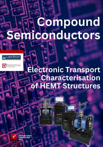
Lake Shore 8400 Hall Measurement System The Lake Shore 8400 Series can be used with both DC and AC field Hall measurement methodologies to facilitate the broadest range of research applications. The system includes fully integrated instrumentation, a magnet and power supply, plus software that dramatically helps you increase your research productivity and provides results that you can trust.
Learn more about Lake Shore 8400 Series
Features of the 8400 Series Ideal for variable temperature measurement and mobilities from 1 to 106 cm2/V s Optional AC field extends mobility measurement range down to 10-3 cm2/V s Maximum DC fields to 1.67 T (8404) and 2.25 T (8407) Optional AC fields to 1.18 T (8404) and 1.31 T (8407) Standard resistance range of 0.5 mΩ to 10 MΩ High resistance option widens range to 200 GΩ Low resistance option significantly reduces resistance noise floor Temperatures from 15 K to 1273 K Also available as an option for the CRX-VF cryogenic probe station
When used with the AC field measurement option, the system is ideal for use with emerging class of materials that typically have mobilities below 1 cm2/V s—the types of materials with electronic properties that can be difficult or impossible to measure with traditional DC field Hall methods. These include many contemporary semiconductor and electronic materials, such as photovoltaic (solar cell) and thermoelectric materials, new display technologies, and organic electronics.
Want to learn more about Lake Shore? Contact our Technical Director: Dr. Shayz Ikram Telephone: (01372) 378822 Email: shayz@qd-uki.co.uk
Read More In Our FREE Magazine