
9 minute read
New Desktop SEM Helps Improve Quality Control, Production Efficiency and Material Cleanliness

Source: ATA Scientific
New Phenom ParticleX SEM
To maintain an effective, cost-efficient operation, a growing number of manufacturing companies are establishing scanning electron microscopy (SEM) systems in-house. The ability to carry out high resolution imaging quickly, and easily, to assess the structure, surface morphology, in addition to chemical verification can help support and improve product development and process control.
Easy-To-Use, Multi-Purpose Desktop SEM
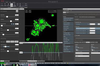
The Thermo Scientific Phenom ParticleX Desktop SEM is a versatile solution for high-quality analysis, that is both simple to operate and fast to learn, opening up the use of particle and material analysis to a wider group of users. The system requires little training and no expert oversight, and is automated for multiple sample analysis. Its ease-of-use, rapid sample preparation and handling, produce unparalleled time to data. Users can obtain high-quality images in just 40 seconds—three times faster than other desktop SEM systems. With an improved resolution of 10 nanometres, it enables even more resolving power, and the ability to explore large samples of up to 100 by 100 millimetres. When compared to the more common tungsten filament electron sources, its Cerium hexaboride (CeB6) electron source is longer lasting with higher brightness. The standard detector in the Phenom ParticleX Desktop SEM is a four-segment backscattered electron detector (BSD), that yields sharp images and provides chemical contrast information. An optional secondary electron detector (SED) collects low-energy electrons from the top surface layer of the sample, exposing detailed sample surface information. The SED is ideal for applications where topography and morphology are important, such as when studying microstructures, fibers or particles.
Elemental Mapping and Line Scan
In addition to fast, high-resolution imaging, the Phenom ParticleX has an integrated energy dispersive X-ray diffraction (EDX) detector for elemental analysis. A simple click on the spot of interest will provide a list of elements present using live energydispersive X-ray (EDX) analysis. Elemental distribution can be visualised with the elemental mapping and line scan option, which is especially useful for coatings, paints and other applications with multiple layers for analysing edges and cross sections. The all-new 24-inch diagonal user interface, combines what were once separate screens for images, and analyses them into a single full-screen image, providing faster and convenient access to information.
Additive Manufacturing, Steel Manufacturing and Technical Cleanliness
The ParticleX SEM (based on the Phenom XL-G2) offers a growing range of fully automated solutions, to help with specific industries and applications. These include particle analysis of metal powders at the microscale for the additive manufacturing industry, investigating inclusions in steel, and confirming that components fulfill technical cleanliness specifications according to VDA19 or ISO16232 standards. Users can monitor particle size distributions, revealing individual particle morphology, and identify foreign particles, providing great insights into production processes and environments.
For further information, contact us.
ATA Scientific Pty Ltd
+61 2 9541 3500 enquiries@atascientific.com.au
Left: Poor powder characteristics can lead to 3D-printed failures.
Below: Automated Energy Dispersive X-ray Spectroscopy (EDX) and Particle Analysis.
Building New Knowledge of Advanced Materials in Extreme Environments
Source: Sally Wood
Molten salt systems are being explored as next-generation low-emission energy generation systems, as well as energy storage systems, due to the superior. physical properties and the safety advantages of molten salts. A study published in Corrosion Science, led by UNSW student, Alexander Danon, and Dr Ondrej Muránsky identified the microstructural characteristics of a nickelmolybdenum-chromium alloy (GH3535) that accounted for its corrosion resistance in a metal used both as a structural material and for weld joints. Danon won third place at the Materials Australia NSW 2019 undergraduate student presentation competition with this research. Dr Muránsky is the Research Program Manager for the Reactor Systems group. The group is focused on the development, performance and degradation of materials in extreme environments, such as hightemperature, radiation, and molten salt corrosion, of near-future energygeneration and energy-storage systems, in Nuclear Fuel Cycle research at ANSTO. “Understanding the corrosion performance of structural materials, and their weld joints, is of technological importance in the design of molten salt-based energy generation and energy storage systems,” Dr Muránsky said. In general, the degradation of salt-facing materials in molten salt environments is known to be brought about by the thermodynamically-driven leaching of alloying elements, which is enhanced by the salt impurities and galvanic interactions between dissimilar metals. The investigators, however, reported that microstructural characteristics of an alloy, such as grain size, can further
An international research collaboration between the University of New South Wales (UNSW), the Shanghai Institute of Applied Physics and ANSTO, has provided insights into the performance of an advanced material for use in the high-temperature environment of molten salt systems.
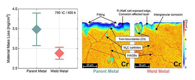
promote leaching of alloying elements, and thus accelerate their molten salt corrosion—leading to an increased material mass loss over time of exposure. The research examined the corrosion behaviour of the alloy GH3535, and its welds, in fluoride molten salt (FLiNaK), which has a low melting point, high heat capacity, and chemical stability at high temperatures. In an experiment conducted by Dr Inna Karatchevtseva at ANSTO, samples of the parent and weld metal alloy were immersed in FLiNaK salt for 500 hours at 750°C, simulating the upper-temperature limit for molten salt systems. The investigators then used Electron Back-Scatter Diffraction (EBSD) and Energy Dispersive X-ray Spectroscopy (EDS) techniques to characterise the chemical composition, and investigate the microstructure of the parent and weld metals after exposure to FLiNaK salt. “The parent metal lost more mass than the weld metal, suggesting a stronger corrosion attack,” Dr Muránsky said. EBSD and EDS revealed significant differences in the microstructure of the alloy matrix, in both the parent metal and the weld metal, following immersion in FLiNaK. The weld metal microstructure was characterised by large elongated grains, growing in the direction of the heat flow during the welding process, while the parent metal featured much smaller equiaxed grains. “Hence, the parent metal had a significantly higher density of High Angle Grain Boundaries (HAGBs), which are known to promote the diffusion of the present alloying elements towards the salt-alloy interface, and thus promote dealloying of the near-surface corrosion-affected layer of the alloy,” Dr Muránsky said. In contrast, the investigators found a greater density of Low Angle Grain Boundaries (LAGBs) and crystal lattice defects (dislocations) in the weld metal; these are also known to promote the diffusion of the alloying elements, but not to the extent of HAGBs.

Furthermore, it was found that HAGBs, which contained large Mo-rich M6C carbides, were impacted by corrosion to a greater extent than those without them. Other contributors to the publications from ANSTO included Tim Palmer, Dr Zhaoming Zhang, Dr Nick Scales and Professor Lyndon Edwards.
Researchers Just Recorded World’s Fastest Internet Speeds Using a Single Optical Chip
Source: Sally Wood
Researchers have achieved the world’s fastest internet data speed – enough to download 1,000 HD movies in a split second – using a single optical chip.
The ground-breaking results, published in Nature Communications by researchers from RMIT University, Monash University and Swinburne University of Technology, could fast-track Australia’s telecommunications capacity and also that of other countries struggling with demand on internet infrastructure. The research team, led by Monash University’s Dr Bill Corcoran, RMIT’s Distinguished Professor Arnan Mitchell and Swinburne’s Professor David Moss, recorded a data speed of 44.2 Terabits per second (Tbps) from a single light source. Professor Mitchell said these speeds were importantly achieved by attaching their new device to existing fibreoptic technology, similar to that used across Australia’s National Broadband Network (NBN). He said the future ambition of the project was to scale up the current transmitters from hundreds of gigabytes per second towards tens of terabytes per second, without increasing size, weight or cost. “Long-term, we hope to create integrated photonic chips that could enable this sort of data rate to be achieved across existing optical fibre links with minimal cost,” Professor Mitchell said. “Initially, these would be attractive for ultra-high speed communications between data centres. However, we could imagine this technology becoming sufficiently low cost and compact, that it could be deployed for commercial use by the general public in cities across the world.”
How it Works
Optical fibres, like those used in the NBN, transmit data on pulses of light. The team’s new device, known as an optical microcomb, creates a rainbow of infrared light, allowing data to be transmitted on many frequencies of light at the same time, vastly increasing bandwidth. Microcombs had not been used in field trials before this study, when researchers placed the fingernail-sized chip – contributed by Swinburne University – onto

Arnan Mitchell creates innovative microchip technologies advancing photonics, fluidics and biomedical research. Optical fibres transmit information as pulses of light.
optical fibres, and sent maximum data down each channel to simulate peak internet usage. That is when data speeds of 40Tbps were reached - about three times the record data rate for the entire NBN network, and approximately 100 times the speed of any single device currently used in Australian fibre networks.
Out of the Lab and Into the Testbed
Significantly, this was tested on 76.6km of ‘dark’ optical fibres between RMIT’s Melbourne City Campus and Monash University’s Clayton Campus. The fibre loop is part of the Australian Lightwave Infrastructure Research Testbed, established with investment from the Australian Research Council, by a consortium led by Professor Mitchell. The testbed allows researchers to investigate innovative new approaches to continually increase the amount of data capacity of existing optical fibre networks. “Having RMIT University as the central node of this world-leading communications testbed gives us insight into the challenges and opportunities for next generation fibre optic communications, in a real-world setting,” Professor Mitchell said. “It also gives us the ability to rapidly test new ideas,” he added.

The test was carried out on a 75km optical fibre loop between RMIT and Monash University in Melbourne.
A Solution for the World’s Insatiable Demand for Bandwidth?
Dr Corcoran, Lecturer in Electrical and Computer Systems Engineering at Monash University, said the unprecedented number of people using the internet for remote work, socialising and streaming, during the coronavirus pandemic, indicated how normal demand for internet infrastructure will look in two to three years’ time. “It’s really showing us that we need to be able to scale the capacity of our internet connections,” he said. “And it’s not just Netflix we’re talking about here – it’s the broader scale of what we use our communication networks for. This data can be used for self-driving cars and future transportation, and it can help the medicine, education, finance and e-commerce industries, as well as enable us to read with our grandchildren from kilometres away.”
