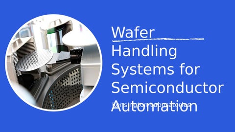
Wafer Handling Systems for Semiconductor Kensington Laboratories Automation
Nowadays, semiconductor and e l e c t r o n i c s c o m p a n i e s a r e o ff e r i n g a full line of industry-leading semiconductor and electronics handling robots. All these robots are built considering their use in cleanroom applications.
Speed, accuracy, and reach make semiconductor robot handl ing ideal for handling delicate semiconductor wafers, LCD panels, organic EL, and solar panels.
High-Performance Wafer Handling Systems
Nowadays, the total productivity of semiconductor fabrication depends on the performance of the robotic systems.
The manufacturers have shifted the directions of wafer handling equipment in the design of mechanical systems with improved manipulating capabilities, optimal application of the wafer handling equipments.
The Manipulating Task In the robotic handling systems (RHS), the common characteristic of the manipulating task is to make constrained straight-line motion at the center of the wafer.
• The straight-line segment is coincident with the longitudinal axis of the equipment (an open cassette, FOUP, a process chamber, etc.). • The linear motion requires a synchronized vertical move to account for equipment placement inaccuracies or deflections of the robotic-arm. • The linear motion requires a synchronized vertical move to account for equipment placement inaccuracies or deflections of the robotic-arm, whereas ideally, the straight-line segment lies in a horizontal plane.
GET IN TOUCH WITH US Website
Fax Number
www.kensingtonlabs.com
510.324.0130
Phone Number 510.324.0126
Company Address
Email Address sales@kensingtonlabs.com
Kensington Laboratories, LLC 6200 Village Parkway Dublin , CA 94568