International Research Journal of Engineering and Technology (IRJET) e ISSN: 2395 0056

Volume: 09 Issue: 07 | July 2022 www.irjet.net p ISSN: 2395 0072
International Research Journal of Engineering and Technology (IRJET) e ISSN: 2395 0056
Volume: 09 Issue: 07 | July 2022 www.irjet.net p ISSN: 2395 0072
2
1PG Scholar (M.Tech), Dept. of Electronics and Instrumentation Engineering, Odisha University of Technology and Research (OUTR), Bhubaneswar, Odisha, India
2Assistant Professor, Dept. of Electronics and Instrumentation Engineering, Odisha University of Technology and Research (OUTR), Bhubaneswar, Odisha, India ***
Abstract In this study, we have signified and interpreted various RF in preference to analog performance of a 80nm gate length AlGaN/GaN metal oxide semiconductor high electronmobilitytransistorgrownonincreasing K dielectric oxide material with numerical modeling based on TCAD simulation. WidebandAlGaN andnarrowbandGaN layersare used as the device channel in single gate devices, along with SiO2, Al2O3, HfO2 are used as the high K gate dielectrics. For improve DC performance, low gate leakage current and improve RF drain current, further double gate and dielectric pocket double gate MOSHEMTs have been designed. Specifically, a HfO2 dielectricMOSHEMTshaveshownexcellent RF performance such as high drain current (ID), high drain conductance (gd), high trans conductance (gm), high intrinsic gain(AV)and maximumcut offfrequency(fT).Alltheresultsof modeling and simulation are created by VISUAL TCAD simulator and hence, obtained up to the mark in terms of analog and sub millimeter wave applications. Here, the effective oxide thickness is specified at 3nm for SiO2, 6nm for Al2O3 and10nmforHfO2 gatedielectricMOSHEMTdevice.The proposedHfO2 gateDP DG MOSHEMT deviceshownhigher up performance like threshold voltage of 2V, high current in drain region (ID) of 8500mA/mm, high output conductance (gd) of 2300mS/mm, high transconductance (gm) of 3600mS/mm, intrinsicgain(AV)of21.82dBandmaximumcut off frequency (fT) of 1.95THz at VDS 5V corresponding to SG MOSHEMT and DG MOSHEMT. The performance of the device is significantlyenhancedbythehigh KAlGaN/GaNbasedDP DG MOSHEMT.
where they will be restricted close to the polarization procured electric field to produce a fine conduction layer. ThissurfaceofelectronsisdeclaredastheTwo Dimensional Electron Gas (2DEG). In contrast to the MOS Field Effect Transistor (MOSFET), electrons from 2DEG can move withoutcollidingwithimpuritiesbecausetheGaNlayeris undoped.Asaresult,thetransistorcanachievehighelectron mobility,whichshouldleadtolowernoisefigures[1 3].The firstHEMTtobemanufacturedwasaGaAs/AlGaAsHEMT. High frequencyperformanceisoftenbetterindeviceswith moreindium,althoughgalliumnitrideHEMTshavegained popularity in recent years due to their high power performance[3].TheadvantagesofHEMTscomprisetheir highgain,whichdrivesthemcompetentasamplifiers,high level switching speeds made possible by the fact that majoritycarriersdominatethechargecarriersinmodulation doped FETs (MODFET), while minority carriers are only moderately involved, and exceptionally low noise values generated by the fact that current fluctuation in these devicesisminimalincomparisontootherdevices[4,5]
The heterojunction is created by two distinct materials, namelyaluminiumgalliumnitrideandgalliumnitride,inthe High Electron MobilityTransistor(HEMT),toonotedasthe two dimensional Electron Gas Field Effect Transistor (TEGFET) and the Heterostructure Field Effect Transistor (HFET)[1].Apotentialwellformsintheconductionbandon theGaNsideoftheinterfaceattributabletothesignificant bandgap energy contrast in the middle of AlGaN andGaN. TheAlGaN layer'selectrons will transfertothe GaN layer,
Whencomparedtoothermaterials,theGaNmaterialhas a variety of special characteristics. For instance, its breakdownfieldisasubstantiallylargerthanGaAsandSi, andits electron mobilityis approximatelytwice ofsilicon. GaN's huge bandgap also makes it possible for a GaN transistor to operate at high temperatures (like 300 °C), whereasthesilicondevice'sfunctionalityisconstrained[1 4].GaN baseddeviceshave manybenefits,including good energydensity(>1000mW/mm),multi octaveradioband, high upefficiency(>50%),linearity,moderatephasenoise andlownoisefactors.GaNhasanhighdegreeofpolarityand isapolarmaterial. Asaresult,theendfacesofthecrystal accumulate sheet charge. Although it's possible that the overall channel charge will be three to four times greater thanthatofanAlGaAs/GaAsbasedHEMT.Theresearchis crucialforcreatingamodelforhigh levelspeedandpower applications[5,6].
Single gateMOS HEMTsimulationandfabricationhave been the subject of several studies [7, 8]. Device performance has improved in devices with several heterostructures, including AlGaN/GaN, InP/InGaAs and AlInN/GaN [4][7][8]. The impression of different high K gatedielectric,likeHfO2,Al2O3 andZrO2 onthegateleakage
International Research Journal of Engineering and Technology (IRJET) e ISSN: 2395 0056
Volume: 09 Issue: 07 | July 2022 www.irjet.net p ISSN: 2395 0072
currentwere exploredin[8 10].Also,theeffectoflow K dielectricoxidewasinvestigatedin[16,17].Pardeshietal. [15]havedetailedtheDCinvestingationofanunderlapping dual gate MOS HEMT and comparability with a silicon underlapMOSFET.GatestackedanddoublegateMOSHEMT andMOSFETwasalsoanalyzedin[9 14].Differentdevice structuressuchasgaterecessedMISHEMTwasdesignedand investigated in [18]. By taking different gate shapes and atomic layer deposition of different oxides in AlGaN/GaN MOHEMTwasdesignedin[19].
Thedouble gatecontrollabilityin[11]improvescurrent densityandtransconductance,whichimprovesthemodel's performance in expressions of half power frequency (fT), higherfrequencyofoscillation(fmax),andnoiseparameters comparedtoitssingle gateequivalent.In[20],GAAMOSFET anddielectricpocketGAAMOSFEThavebeencomparedand found that due to dielectric pocket DPGAA has better immunity towards SCEs and also leakage current is seen suppressedwithtemperaturevariation.
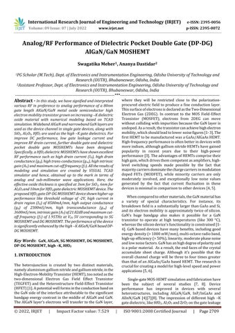
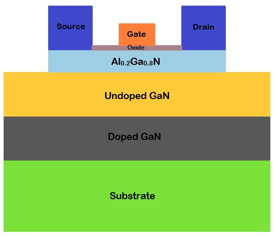
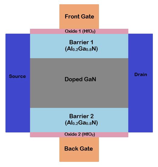
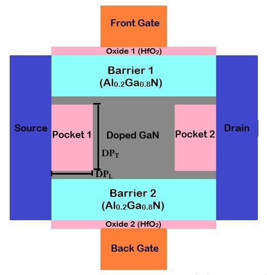
Thecategorizationofpaperisasfollows.Withthehelpof various oxide materials, we have shown the AlGaN/GaN basedsinglegateMOSHEMT.Wefurthersimulateddouble gate and dielectric pocket double gate MOSHEMTs to compare and evaluate the analogand linearity performances. The device architectures and modelling equationsaredescribedinSectionsIIandIII.InSectionIV, thesimulatedresultsofSGMOSHEMTsarecomparedand discussed. By keeping the same device dimensions, the transfercharacteristicsofSGMOSHEMTarecomparedwith DGandDP DGMOSHEMTs.FinallyinSectionV,thefinding isexplained.
interpolation method, the physical properties of
X X AlGaN materialcanbeexpressedas,
In table 1, effective oxide thickness (EOT), represented by TOX,isthegateoxidethicknessoftheSiO2layerofatransistor that would be needed to attain comparable electrical
2022, IRJET | Impact Factor value: 7.529 | ISO 9001:2008 Certified Journal
International Research Journal of Engineering and Technology (IRJET) e ISSN: 2395 0056
Volume: 09 Issue: 07 | July 2022 www.irjet.net p ISSN: 2395 0072
performance as the high K material is employed. The effective oxide thickness can be calculated using following formula, 2 highhighEOT = SiO k k
k t k (2)
Table 1: Oxidethicknessofdifferentdevicestructures
Oxide Material SG MOSHEMT DG MOSHEMT DP DG MOSHEMT EOT TOX EOT TOX EOT TOX SiO2 3nm 3nm Al2O3 3nm 6nm HfO2 3nm 10nm 3nm 10nm 3nm 10nm
PARAMETER NAME Single Gate Double Gate Dielectric Pocket Double Gate
Length of gate (Lg) 80nm 80nm 80nm
Length of source (Ls) 100nm 100nm 100nm
Length of drain (Ld) 100nm 100nm 100nm
Lengthofchannel (Lc) 200nm 200nm 200nm
Draindoping (n+type)(Nd) 1018 cm 3 1018 cm 3 1018 cm 3
Source doping (n+type)(Nd) 1018 cm 3 1018 cm 3 1018 cm 3
Channel doping (ptype)(Na) 1012 cm 3 1012 cm 3 1012 cm 3
Gate source spacing(Lgs) 100nm 100nm 100nm
Gate drain spacing(Lgd) 100nm 100nm 100nm
Barrierthickness (TBOX) 50nm 50nm 50nm
Undoped GaN thickness(TUOX) 100nm
C dopedGaN (ptype)(Na) 1016 cm 3 1016 cm 3 1016 cm 3
ForinvestigatingtheanalogasanalternativeRFperformance of theSG,DGand dielectric pocket doublegate MOSHEMT devices,alltheparameterssuchas,gatelength,source/drain length, HfO2 oxide thickness, barrier, and GaN channel thicknessarekeptsameassinglegateMOSHEMT.
Fig 1(c):HfO2 dielectricpocketdoublegateMOSHEMT structure
The gate voltage at which the least carrier charge density extendsaspecificesteemtobringoffswitchontheonstateis known as the threshold voltage (VT). The constant drain current(ID)approachofVT extortion,whichisoftenusedin numericalsimulationandinvestigationalestimations,isequal tothisdefinition[21].
Thethresholdvoltagecanbedemonstratedas,
Where, GC istheworkfunctiondistinctionconnectingthe gateandthechannel, F istheFermipotentialofthegate, BQ is the depletion region charge density, 2DEG Q is the 2DEG region charge density and OXC is the oxide capacitance.
Dependingonthegatematerial,theworkfunctiondifference forpolysilicongateis, (Substrate)(Gate)GCFF
Fermipotentialforthep typesubstrateis,
International Research Journal of Engineering and Technology (IRJET) e ISSN: 2395 0056
Volume: 09 Issue: 07 | July 2022 www.irjet.net p ISSN: 2395 0072
(5) The depletion region charge density can be calculated by usingfollowingformula.
(6) Here,thedepletionregionchargedensityis 8.83×10 8C/cm2 andtheFermipotentialforpolysilicongateis0.55V. The2DEGregionchargedensitycanbecalculated,
(8)
Here, r isrelativepermittivityordielectricconstant, o is permittivityoffreespace,and ox t isoxidethickness. GSV and CHV aregatetosourcealongwithchannelvoltages.
The drain current equation has been derived under the followingvoltageassumption[21].
Here, GSV and DSV aregatetosourcealongwithdrainto sourcevoltages, GDV isgatetodrainvoltageand DSATV is saturationdrainvoltage. Now, OXC and TV from Equation (8) and (3) can be calculatedindraincurrentequationsforMOSHEMTinlinear mode.
(11)
Forcut offregion, 0 DI ,Where GST VV (12)
Theoutput conductance(gd),trans conductance(gm),trans conductancegenerationfactor(TGF),intrinsicgain(AV),and cut offfrequency(fT)areultimatecrucialfactorsintermsof analog/RFperformance[6].
Thefractionofthechangein DI tothechangein GSV with steady DSV iscalledgatetransconductance(gm).Similarly, theratioofdraincurrent DI variationtodrainvoltage DSV andconstantgatevoltage GSV isknownasoutputordrain conductance(gd) Thenumericalequationshasbeenusedto measuretrans conductanceareasfollows: D m GS
I g V
,Where GSV isconstant. (14)
I g V ,Where DSV isconstant. (13) D d DS
The transconductance generation factorconveys how well thecurrentisusedtoproduceaspecific transconductance value.ThemathematicalequationusedtomeasureTGFis, m D
g TGF I (15)
The intrinsic gain is directly corresponding to the transconductanceandtothevalueofthedrainresistor. 0
g A g Agr
m V d Vm
(16)
Where, 0r isdrainresistor.
Cut offfrequencyorbreakfrequency(fT)isoneofthemost significant factors in determining the device's RF performances.Generally,fTisthefrequencyofaninputsignal atwhichthecurrentgainisunity[6]. 2 m T g
g f C
Where,gatecapacitance gox CCWL
International Research Journal of Engineering and Technology (IRJET) e ISSN: 2395 0056
Volume: 09 Issue: 07 | July 2022 www.irjet.net p ISSN: 2395 0072
Theprecisionandeffectivenessofamodelstructuredepend ontheprecisemeshing,size,andparameterselectionwith precisemeasurements.Afinemeshingisemployedfordevice simulationsatkeyplaceslikethechannelandsource/drain edge.Foreachandeveryproposedstructure,theresultsare produced.
Inthissection,thesimulationresultsofSGdevicewiththree different oxide materials are compared and described. Figure2(a),2(b)and2(c)representagoodmatchbetween simulated and theoretical output current drain voltage characteristic curves (ID VD) of SiO2, Al2O3 and HfO2 gate dielectric MOSHEMT in linear scale for different gate voltages. The mobility of carriers, which is influenced according to the doping concentrations, is an important factorofthedraincurrent.
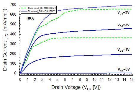
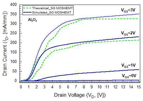
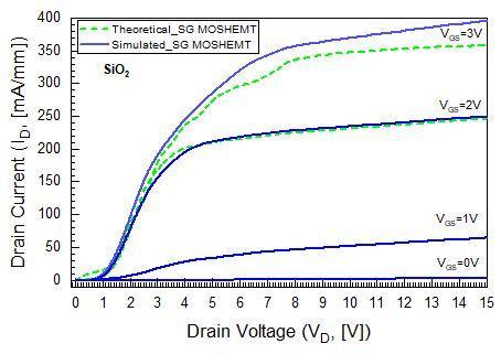
The GaN/AlGaN based SG devices have appeared high electronmobilityinthescale100to800cm2/V sec.Figure 2(c)displayshighestIDatVGS=3Vissimulatedat700mA/mm forHfO2 gatedielectricMOSHEMTwhileforSiO2 andAl2O3, IDmax are 400mA/mm and 350mA/mm. It reveals that the HfO2 gate dielectric layout has an elevated ON current as comparedtoSiO2 andAl2O3 gatedielectric structures.The HfO2 device indicated a highest current density of 440mA/mmatVGS=2Vand180mA/mmatVGS=1V.Thethree differentoxidematerialsstructureddevicesarepinched off completely which means GST VV and the devices are in OFFstateatVGS=0V.
Figure 3 displays the drain conductance drain voltage characteristic curves (gd VD) of SiO2, Al2O3 and HfO2 gate dielectric MOSHEMT for VGS=3V. Maximum output conductanceatVGS=3Vis170mS/mmforHfO2gatedielectric MOSHEMT while for SiO2 and Al2O3, gdmax are 100mS/mm and115mS/mm.
Fig 2(a):ID VD characteristiccurvesofSiO2 atgate voltages0Vto3V.
Fig 2(b):ID VD characteristiccurvesofAl2O3 atgate voltages0Vto3V.
Fig -2(c):ID VD characteristiccurvesofHfO2 atgate voltages0Vto3V.
International Research Journal of Engineering and Technology (IRJET) e ISSN: 2395 0056
Volume: 09 Issue: 07 | July 2022 www.irjet.net p ISSN: 2395 0072
Figure4,representsthedraincurrent(ID VG)togetherwith transconductance (gm VG) with respect to gate voltage characteristiccurvesofSiO2,Al2O3 andHfO2 gatedielectric MOSHEMTinlinearscaleatconstantdrainvoltage5V.Here, the ON current elevates as gate dielectric constant of the structureincreases.TheOFFcurrentdecreasesastheVTalso decreases.Duetoincreaseindielectricconstant,capacitance oxide also increases and hence, the drain current reaches maximum at high K dielectric. This proves the equations (10)and(11),inwhichdraincurrentisdirectlyproportional to dielectric constant and capacitance oxide and inversely proportional to threshold voltage. For output current gate voltage(ID VG),figure(4)showsmaximumdraincurrentis 800mA/mmforHfO2gatedielectricMOSHEMTwhileforSiO2 and Al2O3, IDmax are 320mA/mm and 350mA/mm. For transconductance gate voltage (gm VG), maximum transconductance at VDS=5V is 370mS/mm for HfO2 gate dielectric MOSHEMT while for SiO2 and Al2O3, gdmax are 190mS/mmand160mS/mm.
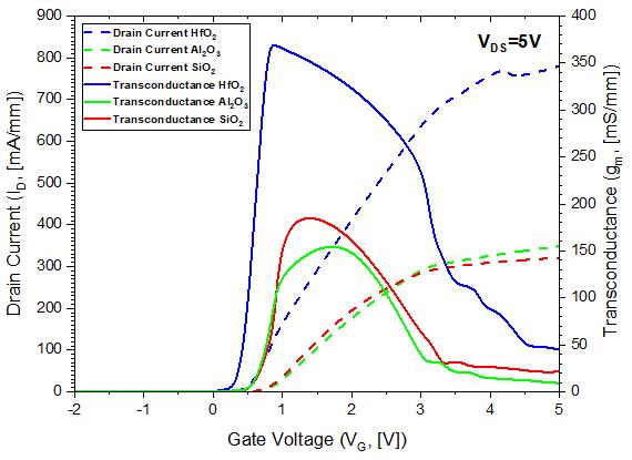
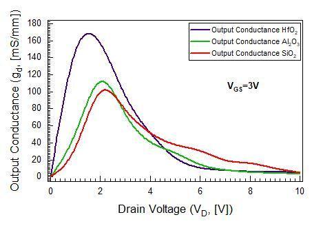
Fig 5:Comparative(fT VG)characteristiccurvesbetween SiO2,Al2O3,andHfO2 dielectricSGMOSHEMTs
Table -3: ComparativeanalysisofSiO2,Al2O3 andHfO2 gatedielectricSGMOSHEMT
OxideMaterial SiO2 Al2O3 HfO2 DielectricConstant(K) 3.9 8.5 25
ID(Max.)atVGS=3V[mA/mm] 400 350 700 ID(Max.)atVDS=5V[mA/mm] 320 350 800 gd (Max.)[mS/mm] 100 115 170 gm (Max.)[mS/mm] 190 160 370 fT (Max.)[GHz] 145 120 180
Fig 3:Comparative(gd VD)characteristiccurvesbetween SiO2,Al2O3,andHfO2 dielectricSGMOSHEMTsatVGS=3V
Figure(5)representsthecutofffrequency gatevoltage (fT VG) characteristics curve, which shows maximum fT at 180GHzforHfO2gatedielectricMOSHEMT.But,theSiO2gate dielectric has better frequency as compare to Al2O3 gate dielectric.Intransconductance(gm)plot,SiO2gatedielectric hasalsobettertransconductancethanAl2O3 gatedielectric. Hence, it demonstrates that transconductance is directly proportional to cut off frequency, which satisfies the equation(17).
Fromthetable(3),itisobservedthat,outofthesethree structures, HfO2 gate dielectric MOSHEMT has shown excellentDCandanalogperformance. Theprimarycauses responsibleforusinghigh Kdielectricmaterialsarelarger physicalthicknessthanSiO2,andprovidehighONcurrents.
4.2 DC and Analog/RF performance of HfO2 gate dielectric single gate, double gate and dielectric pocket double gate MOSHEMTs
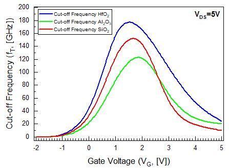
Fig 4:Comparative(ID VG)and(gm VG)characteristic curvesbetweenSiO2,Al2O3,andHfO2 dielectricSG MOSHEMTs
Considering analog/RF performance, the most important parameters are the trans conductance (gm), output
International Research Journal of Engineering and Technology (IRJET) e ISSN: 2395 0056
Volume: 09 Issue: 07 | July 2022 www.irjet.net p ISSN: 2395 0072
conductance(gd),trans conductancegenerationfactor(TGF), intrinsicgain(AV),andcut offfrequency(fT)tobecompared andanalyzedbetweenHfO2gatedielectricsinglegate,double gateanddielectricpocketdoublegateMOSHEMTs.
Figure 6, shows an appropriate match between the comparativesimulatedandtheoreticalthresholdvoltagesof SiO2,Al2O3 andHfO2 dielectricsinglegateMOSHEMTs,HfO2 dielectricDGandDP DGMOSHEMTs.Itisobservedthat,SG devicestructureshavepositivethresholdvoltages,whereas DG and DP DG device posses negative VT. So, for normally OFF operations SGMOSHEMT structure istheappropriate choiceduetopositivethreshold.Aswecansee,ifdielectric constant increases threshold voltage decreases and hence, draincurrentalsoincreases[20].Infigure7(a),atVGS=3V, DP DGdevicehasthehighestdraincurrentof8000mA/mm andoutputconductanceof2300mS/mmascomparedtoDG MOSHEMT. At VDS=5V, figure 7(b) compares the transfer propertiesofHfO2 dielectricSG,DGandDP DGMOSHEMTs onalinearscale.Fromthisresult,theION/IOFFcurrentratioin DP DGMOSHEMTwassubsequentlyimprovedwhichclearly shows that the existence of dielectric pockets reduces the chargesharingattheinterfacesofthesource channelaswell asdrain channeland,consequently,theIOFF current[20].
Figure (8), explores by varying in transconductance generation factor of HfO2 dielectric SG, DG and DP DG MOSHEMTsagainstgatetosourcevoltageatVDS=5V.Itcan benoticedfromthefigure(8)that,SGMOSHEMThashigher TGF,whichisconsideredtobehighlyefficient.HigherTGF leadsthedeviceperformancesincreasesandcanoperateat low supply voltage. For TGF between 10V 1 and 5V 1 variationswithVGSfrom 1Vto1.5Vtypicallyusedforanalog performance[20].
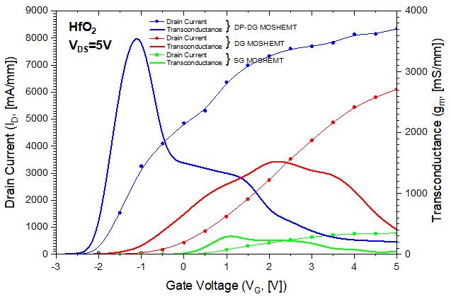
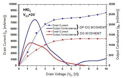
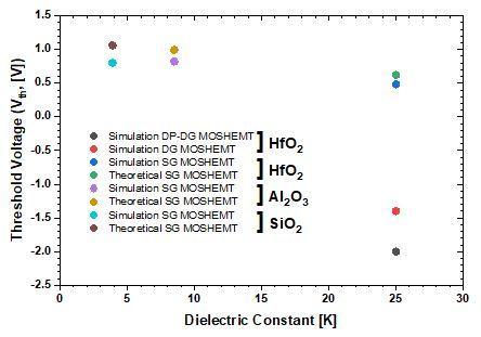
Fig 7(a):Comparative(ID VD)and(gd VD)characteristic curvesbetweenHfO2dielectricDGandDP DGMOSHEMTs
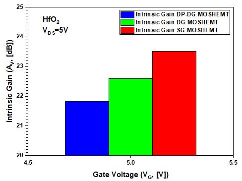
Additionallyshowninfigure(9),relationtogatetosource voltage (VGS) is the device's intrinsic gain, which is the transconductancetooutputconductanceratiofordifferent devicestructuresatVDS=5V.Here,DP DGMOSHEMTreduces thegainwhileimprovingthedevice'slinearity.
Fig 6:Comparisonof(VT K)betweendielectricSG,DGand DP DGMOSHEMTs
Fig 7(b):Comparative(ID VG)and(gm VG)characteristic curvesbetweenHfO2dielectricSG,DGandDP DG MOSHEMTs
International Research Journal of Engineering and Technology (IRJET) e ISSN: 2395 0056
Volume: 09 Issue: 07 | July 2022 www.irjet.net p ISSN: 2395 0072
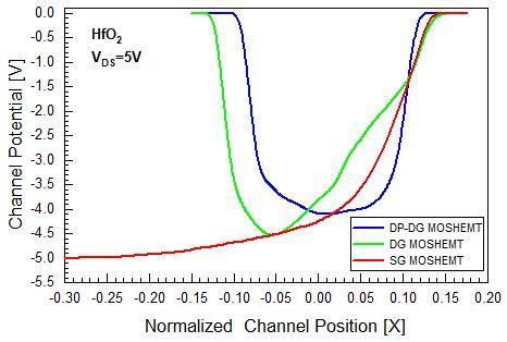
MOSHEMThasbeenthenegligiblechannelpotentialcurve amidstthethreewhichsignifiesthatDGstructuresustains fromminimalamountofhotcarriereffect[22].
Fig -8:ComparativeTGFvariationwithVGS betweenHfO2 dielectricSG,DGandDP DGMOSHEMTs
Fig 10:Comparativecut offfrequencyvariationwithVGS betweenHfO2dielectricSG,DGandDP DGMOSHEMTs
Fig 9:Comparativemaximumintrinsicgainvariationwith VGS betweenHfO2dielectricSG,DGandDP DGMOSHEMTs
For estimating the radio frequency performance of the device, cut off frequency is one of the most significant specifications. From figure (10), the deviation of cut off frequency can be observed in respect of gate to source voltage(VGS)totheorderofVDS=5V.Here,thehighervalueof cut off frequency obtained at 1.95THz for the dielectric pocket double gate device. By virtue of the previous statements,thegmvalueishighforDP DGMOSHEMTandlow for SG MOSHEMT. As per the above reference it is understandable that gm and fT are exactly sustained by the drain current. Figure (11) displays the modification of channel potential across the channel from source to drain sideforSG,DGandDP DGdevicestructures.ForSGmodel, theworkfunctionofgatematerial(NPolySi)isbetteratthe drain edge. But, for DG layout, the work function of gate materialisbetteratthesourcesideandforDP DGlayout,the workfunctionofgatematerialisbetteratsourceaswellas drainend.Thefigure(11)showsthat,atthedrainendDG
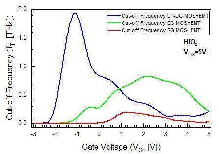
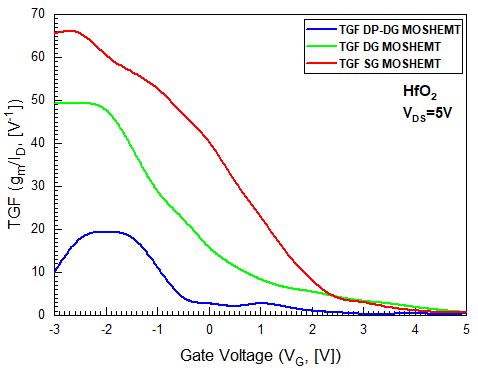
Fig 11:Comparativechannelpotentialdeviationwith normalizedchannelpositionbetweenHfO2dielectricSG, DGandDP DGMOSHEMTs
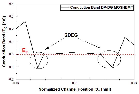
Figure (12), depicts the energy band diagram of the AlGaN/GaN formed DP DG MOSHEMT. The device's conductionbanddeviatesfromtheFermilevel(EF),forminga well across the interface. That well isknown as quantum/ potential well [8]. It shows that, 2DEGhas been formatted with electrons supplied by surface donor states in DP DG device[12].Table(4)comparestheRF/Analogparametersof thisworkusingHfO2dielectric.
International Research Journal of Engineering and Technology (IRJET) e ISSN: 2395 0056
Volume: 09 Issue: 07 | July 2022 www.irjet.net p ISSN: 2395 0072
Fig 12:TheproposedAlGaN/GaNheterostructure based DP DGMOSHEMT'sbandstructureoutline
Table -4: ComparativeanalysisofHfO2 gatedielectricSG, DGandDP DGMOSHEMTs
DeviceStructures Single Gate Double Gate Dielectric Pocket DoubleGate
ThresholdVoltage (VT,[V]) 0.48 1.4 2
ID(Max.)atVGS=3V [mA/mm] 700 4500 8000
ID(Max.)atVDS=5V [mA/mm] 800 6000 8500
gd (Max.)VGS=3V [mS/mm] 170 1200 2300
gm (Max.)VDS=5V [mS/mm] 370 1600 3600 TGF,VDS=5V [V 1] 65 50 19
Intrinsicgain(AV,[dB]) 23.52 22.6 21.82
fT (Max.)[THz] 0.18 0.8 1.95
From the above experiments, it is concluded that for RF/Analogperformancehigh Kdielectricmaterialismore preferable because of its better control over the channel electrons as well as larger physical thickness than low K dielectric.Byusinghigh Kdielectric,theDP DGMOSHEMT structure has been performed better because of dielectric pockettechnology.Evenif,ithasbeenlowTGFandgain,but it provides maximum transconductance and cut off frequency.Simultaneously,itcanbeeasilyseeninSGandDG MOSHEMT, stronger TGF results in improved device efficiencyandpreferablegainperformanceatlesservoltages.
This paper presents a modified study of the analog/RF characteristicsfortheAlGaN/GaNSGMOSHEMTandfurther, DGandDP DGMOSHEMTsarecontemplatedandanalyzed byusingdevicedesignguidelines.Bymaintainingaconstant channel length and gate length, the effects of high K dielectric on device performance have been investigated consideringDC,analog,andRFapplications.Ourcalculated and simulated results in SG device show that HfO2 gate dielectricwillbepreferableforanalogandRFperformance. By keeping the same device dimensions, further HfO2 dielectric DG and DP DG MOSHEMTs have been designed andobserved.WithreferencetoRFandanalogapplications, thedevicesneedtobeoperatedinabovethresholdregime. From the simulated results, DP DG device has lowest thresholdvoltageandhence,IOFFcurrentisalsodecreasing. Due to the implementation of dielectric pocket in DG MOSHEMT,italleviatesthechargesharingattheinterfaces ofthesourceaswellasdrain channel,andhence,ONcurrent ismaximumandobservedat8500mA/mm.Similarly,inDP DGdevicetheoutputconductanceisincreasedby91.66%, and transconductance is enhanced by 125% from DG MOSHEMT. But, in case of TGF and intrinsic gain [AV], SG device has been performed more efficiently and it can be operatedatlowsupplyvoltage.But,itisobservedthatDP DGdevicehasmaximumfrequencyof1.95THz,whichcanbe usedinsub millimeterwaveapplications.Hence,thepresent DP DGMOSHEMTusingHfO2gatedielectricleadstofurther improvement in TGF and intrinsic gain as it is providing superiortransfercharacteristics.TheperformanceofSG,DG, and DP DG MOSHEMTs can be enhanced by adjusting the other device parameters in accordance with the requirementsoftheapplications.
[1] KhanAN,Jena KA,RoutrayS,ChatterjeeG.RF/Analog and Linearity Performance Evaluation of Lattice matched Ultra thin AlGaN/GaN Gate Recessed MOSHEMTwithSiliconSubstrate.Silicon.2022Jan13:1 0.
[2] Zhang,Dabin."CharacterizationofGaNMOS HEMTtrap related effects for power switching applications." (2015).
[3] Mariappan, Revathi. "Drain Charactersitic Analysis of HighElectronMobilityTransistor(Moshemt)." Available at SSRN 3379286 (2019).
[4] Kumar,R.Saravana,etal."DCandRFCharacterizationof InAs based Double Delta Doped MOSHEMT Device." 2018 IEEE Electron Devices Kolkata Conference (EDKCON).IEEE,2018.
[5] Ajayan,J.,Ravichandran,T.,Mohankumar,P.,Prajoon,P., Pravin,J.C.,&Nirmal,D.(2018).InvestigationofDCand
© 2022, IRJET | Impact Factor value: 7.529 | ISO 9001:2008 Certified Journal |
International Research Journal of Engineering and Technology (IRJET) e ISSN: 2395 0056
Volume: 09 Issue: 07 | July 2022 www.irjet.net p ISSN: 2395 0072
RFperformanceofnovelMOSHEMTonsiliconsubstrate for future submillimetre wave applications. Semiconductors, 52(16),1991 1997.
[6] Mohapatra, Sushanta K., et al. "The performance measure of GS DG MOSFET: an impact of metal gate work function." Advances in Natural Sciences: Nanoscience and Nanotechnology 5.2(2014):025002.
[7] Ochi, Ryota, et al. "Gate controllability of HfSiOx/AlGaN/GaN MOS high electron mobility transistor." AIP Advances 10.6(2020):065215.
[8] Zine eddine,T.,Zahra,H.andZitouni,M.,2019.Design andanalysisof10nmT gateenhancement modeMOS HEMTforhighpowermicrowaveapplications. Journalof Science: Advanced Materials and Devices, 4(1), pp.180 187.
[9] EDWIN, LOW KIM FONG. "Characterization and Numerical simulation of Gallium Nitride based Metal oxide semiconductorHighElectronMobilityTransistor withHigh KGateStack."(2012).
[10] Baidya, Achinta, Srimanta Baishya, and Trupti Ranjan Lenka."Impactofthinhigh kdielectricsandgatemetals on RF characteristics of 3D double gate junctionless transistor." Materials Science in Semiconductor Processing 71(2017):413 420.
[11] Panda, Deepak Kumar, et al. "Single and double gate based AlGaN/GaN MOS HEMTs for the design of low noise amplifiers: a comparative study." IET Circuits, Devices & Systems 14.7(2020):1018 1025.
[12] Verma,M.andNandi, A.,2020.Designandanalysisof AlGaN/GaN based DG MOSHEMT for high frequency application. Transactions on Electrical and Electronic Materials, 21(4),pp.427 435.
[13] Kumar, Shubham, et al. "Impact of Source and Drain Underlap on Analog Performance of Double Gate AlGaN/GaNMOS HEMT." 2020IEEECalcuttaConference (CALCON).IEEE,2020.
[14] Chattopadhyay, A., Dasgupta, A., Das, R., Kundu, A., & Sarkar, C. K. (2017). Effect of spacer dielectric engineeringonasymmetricsourceunderlappeddouble gate MOSFET using gate stack. Superlattices and Microstructures, 101,87 95.
[15] Pardeshi, Hemant. "Analog/RF performance of AlInN/GaNunderlapDGMOS HEMT." Superlattices and Microstructures 88(2015):508 517.
[16] Zhu,Gengchang,etal."GaNmetal oxide semiconductor high electron mobility transistors using thermally evaporated SiO as the gate dielectric." Semiconductor Science and Technology 33.9(2018):095023.
[17] Hasan,MdRezaul,etal."Fabricationandcomparative studyofDCandlowfrequencynoisecharacterizationof GaN/AlGaN based MOS HEMT and HEMT." Journal of Vacuum Science & Technology B, Nanotechnology and Microelectronics: Materials, Processing, Measurement, and Phenomena 35.5(2017):052202.
[18] Kim HS, Kang MJ, Kim JJ, Seo KS, Cha HY. Effects of recessed gate structure on AlGaN/GaN on SiC MIS HEMTswiththinAlOxNyMISgate.Materials.2020Mar 27;13(7):1538
[19] Zhou, Hong, et al. "DC and RF performance of AlGaN/GaN/SiC MOSHEMTs with deep sub micron T gates and atomic layer epitaxy MgCaO as gate dielectric." IEEE Electron Device Letters 38.10 (2017): 1409 1412.
[20] Awasthi H, Kumar N, Purwar V, Gupta R, Dubey S. Impact of temperature on analog/RF performance of dielectric pocket gate all around (DPGAA) MOSFETs. Silicon.2021Jul;13(7):2071 5.
[21] Swain, R., K. Jena, and T. R. Lenka. "Modelling of capacitance and threshold voltage for ultrathin normally off AlGaN/GaN MOSHEMT." Pramana 88.1 (2017):1 7.
[22] KashemMT,SubrinaS.Analyticalmodelingofchannel potential and thresholdvoltageof triple material gate AlGaN/GaN HEMT including trapped and polarization‐induced charges. International Journal of NumericalModelling:ElectronicNetworks,Devicesand Fields.2019Jan;32(1):e2476.
2022, IRJET | Impact Factor value: 7.529 | ISO 9001:2008 Certified Journal