1Scientist ‘D’, Ministry of Electronics and Information Technology (MeitY), Government of India
©
3 Project Assistant, IIT Hyderabad, posted at Ministry of Electronics and Information Technology (MeitY)
Key Words: Low Power, MTCMOS, XNOR, High
Abstract The power usage had a significant role in integrated circuits and also enumerated as one ofthetopmost 3 challenges in the world semiconductor devices technology map. The low powered club has become a significant factor in recent changes to VLSI. This paper presents examples of pre designing a low level 2T XNOR unit at low voltages and consume less amount of power that existing design in this paper newly designed XNOR unit is compared with other low power XNOR units. The core determination of new strategy is to reduce usage of power and reduce absolute voltage to achieve low power as well as voltage of supply. In that article, 2T XNOR gate through MTCMOS. This MTCMOS technology without comparison is compared by considering power as a measurement according to different temperature, frequency and voltage. The designed circuits are tested on 32nm technology of XNOR design with MTCMOS technology for minimum usage of power.
Mr. Kamlesh Kumar1 , Mr. Mohit Dahiya2 , Mr. Manoj Kumar3 , Mr. Priyanshu Lakra4
In huge scope joining (VLSI) plan expansion in semiconductor thickness, power utilization and scaling of size of CMOS become a vital imperative. The scattering of power of circuit that designed using CMOS incorporates dynamicaswellasstaticforcedissemination.Atthepoint whenstructureispresentindynamicoperation, power in dynamicmodestays inthe circuit.Acc.to design of CMOS circuit the exchanging and power of short circuit is determined.Dischargingandchargingofthecapacitiveload thatbasespowerswitching aswell aschargingofinterior hub prompts impede scattering. The gate encouraged leakageofsubthreshold,drainandgateleakageandoxide tunneling are the fore most factor of dissipation of power scalevoltageThedisseminationorleakage[1].ThecurrentleakageincrementsasgadgetsizingscalinghappensthatleadstoexpandsthealloutpowerofCMOScircuit[2].powersupplycanbedecreasedbyincreasingthesupply.ThesupplyofDCcurrentalongadimensionalbeganwiththehalfmicrometertechnologybutthesize andincludesbeforetechniquetosupplementarytimemethodadjustingmethodscomparisonTheindividually.powerHere,energyinthedownallowthresholdheaderwherePowertheAbundantreducingThemaintainingpracticesusestechnologystructuregatesemergingMTCMOSAttemptssooftheelectricfieldcauseseffectonthespeedinessofcircuit,therequiredtimeforperformingexecutionreduces[56].todesignhighspeedandlowpowercircuitsusingthatleadstohighspeedexecutionofcircuits,asapromisingoptionforbuildinghighspeedlogicthatconsumeslesspowerthanpreviousexistingCMOSdesign.MTCMOSisanefficientstepbystepdeliverslowpowerandhighperformancedesignhighandvoltagetransistorsaswellasthisstrategythattoreducelowflowofemergencymodewhilecircuitperformance[4].lifetimeofbatteryofacellphonecancontrolledbyorstoppingtheirspillageduringrestmode.staticmethodologieshavedevelopedtodecreasecurrentinstaticformincircuitofCMOSdesign[3].Thegatingmethodsaregenerallyutilizedinlatesituation,powerinstaticformbeingabletodecreasedbyPMOSorNMOSfooterwithhighvalueofvoltageatlevel.Throughturningofforonofpowerswitches,measureoftheexchangingenergyabletobroughtthroughutilizingtheinnovativepowergatingalongchargereusingprocedure.Atbothinsleepingaswellasworkingmode,thesharingofchargeofexchangingofoccursinbetweenavirtualVSS&effectiveVDDlines.effectiveVSSandVDDconnectionareattachedtoandgroundthroughtheNMOSandPMOSchargereusedplanisabledropextraenergyasinwithmodeofrestthanconservativeforcegatingdeprivedofutilizingsharingofchargescheme.InvirtualVSSandVDDlines,thechargereusedofpowergatingwantsextratimeandthuslyawakenisextensive.Restmodeoffinegrainleakageisthanthecoarsegrainleakage.Ascomparedconventionalpowergatingtechniquesdualpowerisfast[5].Variousfactorsshouldbeconsideredsuccessfulimplementationofthecircuitwhichleakageofpowergate,switchingcapacitance,sizeslewrateofpowergate.
Volume: 09 Issue: 03 | Mar 2022 www.irjet.net ISSN: 2395 0072 2022, IRJET Factor value: 7.529 9001:2008
4Project Engineer, CDAC Hyderabad, posted at Ministry of Electronics and Information Technology (MeitY) ***
International Research Journal of Engineering and Technology (IRJET) e ISSN: 2395 0056

| Impact
Certified Journal | Page1109
2Project Engineer, CDAC T, posted at Ministry of Electronics and Information Technology (MeitY)
p
| ISO
Comparative Analysis and Designing of High Performance and Low Power XNOR Gate Circuit using Hybrid Sleep-Stack (MTCMOS) Technique
1.INTRODUCTIONPerformance,CMOS
2.Hybrid sleep-stack (MTCMOS)technique
FIG 2:- Schematicof2TXNORgateofHybridsleep stack (MTCMOS)techniqueinS EditofEDATool
p ISSN: 2395 0072 2022, IRJET Impact Factor value: 7.529 9001:2008
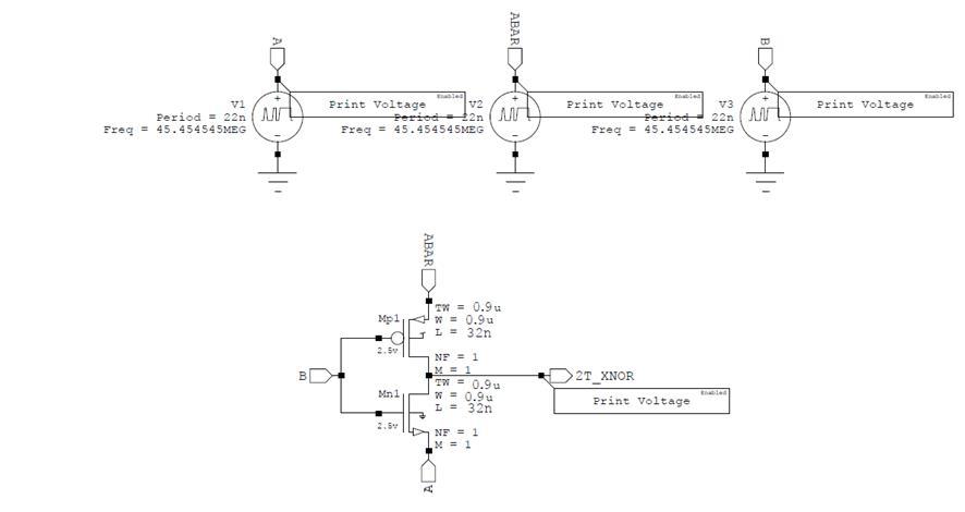
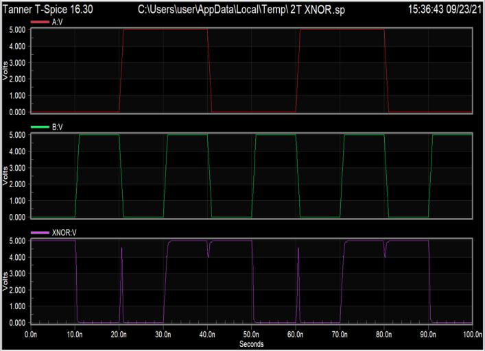
Whenoneoftheinputsishigh(A=0,B=1)or(A=1,B=0),in thiscasetheNMOSisONbutoveralloutputislow(Out=0) ignoringtheeffectofPMOSbeingON.Whenboththeinputs willarehigh(A=1,B=1)thentheNMOStransistorsareONwhichdrivethehighoutputsignalandPMOSisOFF.
The designed circuit of XNOR gate as shown in figure, contains two transistors one PMOS, PM1 and one NMOS, outputofswitchedANM1.OperationoftheXNORgateisdependentontheinputsandB.Whenboththeinputislow(A=0,B=0)thenNMOSisOFFandPMOSisswitchedONduetolargevoltagegatethenthreshold.AndPMOSinthiscasepasshigh(Out=1)logic.
Certified Journal | Page1110
| ISO
FIG1: Schematicof2TXNORgatedesignedinS Editof EDATool
Volume: 09 Issue: 03 | Mar 2022 www.irjet.net
|
International Research Journal of Engineering and Technology (IRJET) e ISSN: 2395 0056
©
3. Design of XNOR gate using Hybrid sleep stack (MTCMOS) technique
Thepowergatingmethodisutilizedtominimizedissipation ofstaticpowerofintegratedCMOScircuitbyswitchingthe power supply of the circuit for short interval of time. The power gating technique is also used in the testing of the CMOS circuit. The general working of the power gating method is externally switching of the power supply and alsotechnique,techniquesthestandbyreducethepowerleakage.InmostlyCMOScircuitduringthemode,leakagepowerismaincauseofreductioninefficiencyofthecircuit.ThemajorlyusedpowergatingwhichareusedintheCMOScircuitsaresleepstacktechnique,sleepystacktechniquewhicharecalledMTCMOSpowergatingstructuretechniques.
Thereiseffectontheleakagecurrentatsub thresholdpoint as the geometry of device scales down. Backup leakage current will turn out to be equal to the dynamic power modebatterypowerdissipationinvariousdifferentcircumstances,whichisduetosupplyandthresholdvoltagescaling.Toincreaselifeofthemobiledevices,leakagecurrentatstandbythatcouldreducedwhichisduetohighstandbyperiod
Nowadays,highspeedlowpowerCMOSdesignisthemost stimulating concerns in VLSI technology. As the VLSI technology is increasing towards the scaling reduction of technology, the consumption of static power had twisted intoaremarkableconcern.Thisresearchworktermpaper incorporatesthecomparisonfollowinggatingtechniqueof power reduction such as leakage control transistor technique (LECTOR), stack & sleep strategy, sleepy stack strategy,sleepykeeperstrategy,andsleepykeeperleakage controltransistorstrategy(SK LCT)forreductionofleakage of power [7]. In this paper, XNOR gate is designed with MTCMOS Power gating structure technique considering consumption of power as a parameter by changing versionbeenconsumptionMTCMOSwithfrequency,temperatureandvoltage.Thedesignsareverified32nmdeviceslibraryfiles.A2TXNORgatedesignwithtechniqueresultsoutminimumpowerAllthecircuitdesigningandexecutionshadimplementedwith32nmlibraryfilesonEDATool12.6.
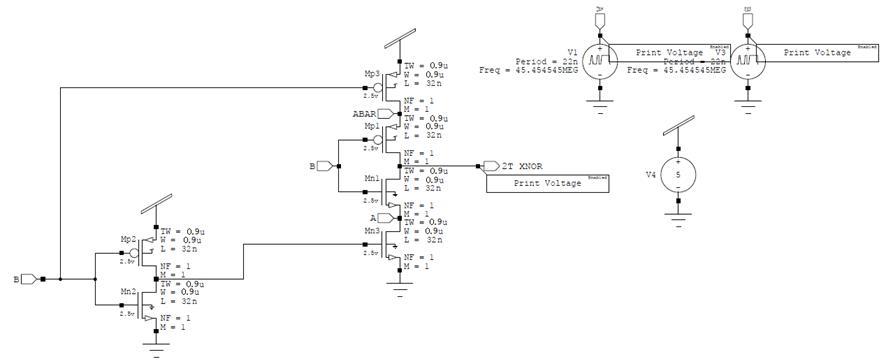
[8]. MTCMOS is one of the utmost operative technique to diminish the power leakage of the circuit. In MTCMOS technique, there are two different modes of operation, standby mode & active mode. It consists of two threshold transistortransistorswhereasingeneralthereisonlysinglethreshold(V t) in the CMOS circuit. There are two types of transistors used in the MTCMOS technique, one is high threshold voltage transistor (i.e., high Vt)) called sleep transistor, which isusedinavertingdissipation ofleakage powerandotherislowthresholdvoltagetransistor(i.e.,low Vt)whichisusedtoenhancetheperformanceofcircuit.One ofthesleeptransistorthatisplacedinbetweenthepull up networkandpowersupplyandotherisplacedbetweenpull GroundtheatconditionLOWstandbyThethesedownandground.Twocomplementarysignalsareappliedtonetworks[1].SEditcircuitshownbelow,operatesinactiveandmode.Inactivemode,whileTBARisHIGHandTisthenboththesnoozetransistorsareturnedON,inthisitworksasnormalCMOScircuit.Duringoperationstandbymode,TisHIGHandTBARisLOWthenitturnsoffsleeptransistors,resultinginhighresistancefromVDDtothatwillreducetheleakagepower.
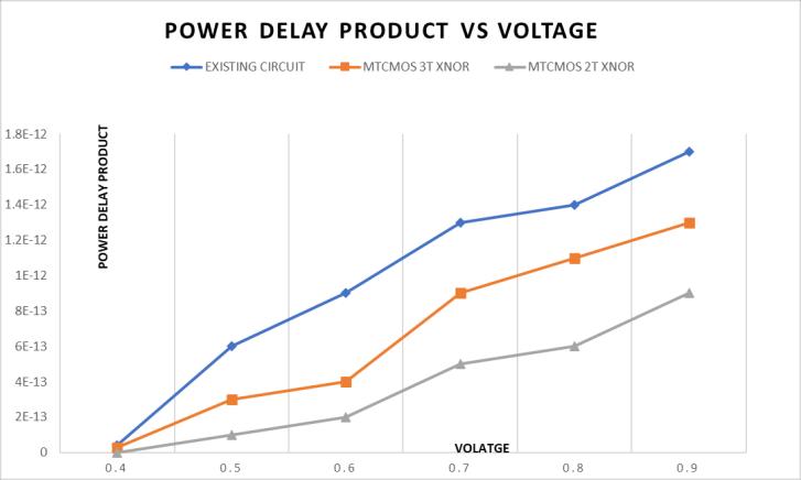
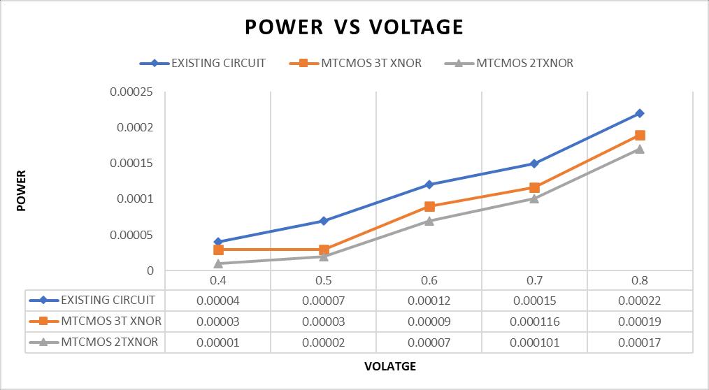
International Research Journal of Engineering and Technology (IRJET) e ISSN: 2395 0056 Volume: 09 Issue: 03 | Mar 2022 www.irjet.net p ISSN: 2395 0072 © 2022, IRJET | Impact Factor value: 7.529 | ISO 9001:2008 Certified Journal | Page1111 4.RESULTS enhanced2TXNORbetweennmAlltheschematicsimulationsareexecutedonEDAtoolat32technologyatdiverseinputvoltagelevelthatrangesin0.3to0.9Vinsmallintervalsof0.1V.Boththecircuitswillbetestedwithsameinputpatterns.TheXNORgatewithMTCMOSisobservedthatitshowsperformancethanthepreexistingXNORgate Table 1: PresentationTableof2TXNORgate (Input)A (Input)B OutcomeEstimated Attainedoutput 0 1 1 0.001 1 1 0 1.001 0 0 0 1.001 1 0 1 0.001 4.1Simulation of thecircuitresults inEDA tool Itisobservedthatusingvariousabove mentionedtechnique hasenhanced temperature sustainabilityandsuggestively power delay product (PDP) & less power at numerous differentinputfrequencies&voltages. FIG 3: Output2TXNORgateofHybridsleep stack (MTCMOS)techniqueinS EditofEDATool MTCMOSdesignedcircuitryhaveadrawbackthatitcauses throughGenerally,minimalescalationofareaasassociatedtotheCMOScircuit.werealizedthedissipationofminimalpowerMTCMOStechnique. Table 2: PowerDelayProductVsVoltageAnalysis (V)VOLTAGE POWER DELAY PRODUCT CIRCUITEXISTING XNORMTCMOS3T XNORMTCMOS2T 0.5 6E 13 3E 13 1E 13 0.6 9E 13 4E 13 2E 13 0.7 1.3E 12 9E 13 5E 13 0.8 1.4E 12 1.1E 12 6E 13 0.9 1.7E 12 1.3E 12 9E 13 Chart 1:PDPVsVoltageofexistingcircuit,MTCMOS3T XNORandMTCMOS2TXNOR Table 3: PowerConsumptionVsVoltageAnalysis (V)VOLTAGE CIRCUITEXISTINGPOWERCONSUMPTION(Watt)MTCMOS3TXNORMTCMOS2TXNOR 0.4 0.00004 0.00003 0.00001 0.5 0.00007 0.00003 0.00002 0.6 0.00012 0.00009 0.00007 0.7 0.00015 0.000116 0.000101 0.8 0.00022 0.00019 0.00017 Chart 2:PowerVsVoltageofexistingcircuit,MTCMOS3T XNORandMTCMOS2TXNOR
[7]HemanthaS,DhawanAandKarH,“Multi thresholdCMOS designforlowpowerdigitalcircuits”,TENCON2008 2008 IEEERegion10Conference,pp.1 5,2008.
| ISO
REFERENCES
[2]Pousia.S,Manjith.R(2018),“Designoflowpowerhigh speed SRAM architecture using SK LCT Technique”, IEEE International Conference on Current Trend towards ConvergingTechnologies,Nov2018.
5.CONCLUSION
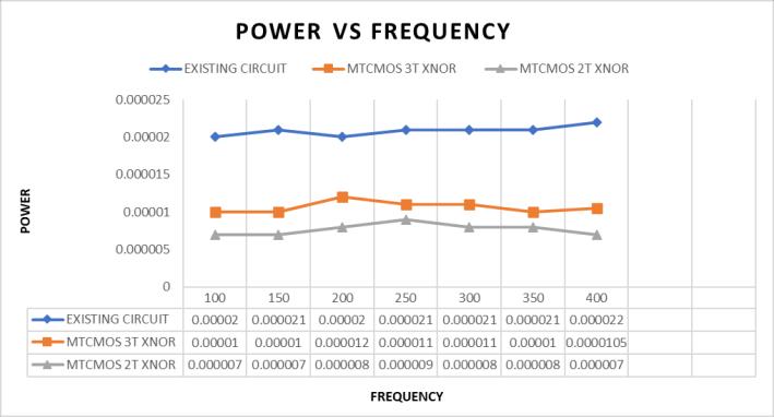
Chart-3: PowerVsFrequencyofexistingcircuit,MTCMOS 3TXNORandMTCMOS2TXNOR
© 2022,
Certified Journal | Page1112
[4]YeapG.K.etal(1998),“PracticalLowPowerDigitalVLSI Design’,KluwerAcademicPublishers”,Norwell,MA,ISBN: 0792380096,pp 233.
p
[8]Q.Zhou,X.Zhao,Y.Cai,X.Hong,“AnMTCMOStechnology forlow powerphysicaldesign”,IntegrationVLSIJ.(2008).
BIOGRAPHIES
Mr. Kamlesh Kumar received B.Tech degree in Electronics & NewTechnologyfromCommunicationEngineering(ECE)MaharajaAgrasenInstituteof,G.G.S.I.P.University,Delhi,Indiain2010.Heis


[3]AndreaCalimera,AlbertoMacii,EnricoMacii&Massimo Poncino(2017),“DesignTechniquesandArchitecturesfor Low Leakage SRAMs”, IEEE Transactions on Circuits and Systems,Vol.59,No.9,Sep2014,pp.1992 2007
e
| Impact
[6] Mutoh S et al, “1 V Power supply high speed digital circuittechnologywithmultithreshold voltageCMOS”,IEEE J.SolidStateCircuits,Vol.30,pp.847 854,August1995.
currently working as Scientist ‘D’ in Ministry of Electronics and Information Technology (MeitY), SystemandincludingStrategicConvergedQTP,differentforTechnologyMeteorologyincludingweatherAssistantofDepartmentserMinistry.variousGovernmentofIndiaandinvolveinR&DactivityintheBeforeJoiningMeitY,hevedinIndiaMeteorological(IMD)underMinistryEarthScienceasScientificandworkonDifferentforecastingactivityRadar,Synop,AviationalsoheservedinHCLasSoftwareEngineertwoyearsandworkedontools,i.e.,LoadRunner,Selenium.HisresearchareaisCommunication,/IndustrialElectronicsIoTandCognitiveRadioIntelligentTransportation(ITS)
The2T withcircuits;circuitslatencystabilitythegateversionexistingXNORgateisdesigned,simulatedandcomparedwithXNORunitsandsimulatedontheTannerEDA16.3instrumenton32nmtechnology.The2TXNORwithMTCMOSissaidtogivebetterperformancethanexistingXNORgate.Itistestedforsuperiortemperatureandprovidessignificantlylowerpowerandpoweratvariousinputvoltagesandfrequencies.MTCMOShaveaslightlyincreasedareacomparedtoCMOSOverall,weachievedthelowestpowerconsumptionMTCMOStechnology.
International Research Journal of Engineering and Technology (IRJET) ISSN: 2395 0056
[1] Pousia .S , Manjith.R (2018), “Proficient Static RAM design using Sleepy Keeper Leakage Control Transistor & PT Decoderforhandheldapplication”,InformacijeMidem: Journal of Microelectronics, Electronic Components and Materials,Vol.48,No.4,pp 197 203.
Volume: 09 Issue: 03 | Mar 2022 www.irjet.net ISSN: 2395 0072 IRJET Factor value: 7.529 9001:2008
[5] F. Catthoor, S. Wuytack, E.DeGreef (1998), “Custom MemoryManagementMethodologyExplorationofMemory Organization for Embedded Multimedia System Design”, KluerAcadamicPublishers,Boston.
Mr. Mohit Dahiya, received B.Tech in Electronics and CommunicationEngineeringfrom Maharaja Surajmal Institute of Technology, affiliated by Guru GobindSinghUniversityinyearof 2019 and currently pursuing M.Tech in Electronics and Communication from University School of Information Communication and Technology (GGSIPU).Heiscurrentlyworking as Project Engineer in Centre Development of Advance Computing (C DAC), posted at
Mr. Manoj Kumar, received TechnologyElectronicsHyderabad,assamepublishedpower(GGSIPU).HeCommunicationschoolEngineeringElectronicscurrentlyUniversityGuruEngineeringEngineeringB.TechinElectricalandElectronicsfromNorthernIndiacollege,affiliatedtoGobindSinghIndraprasthaintheyearof2018andpursuingM.TechinandCommunicationfromUniversityofInformationandTechnologyhasworkedonlowapplicationdevicesandtheresearchontheandHeiscurrentlyworkingProjectAssistantinIITpostedatMinistryofandInformation(MeitY)onproject
©
Ministry of Electronics and Information Technology (MeitY) on projects of Intelligent MethodologyVerificationVerification,RandomMethodologies|VLSI|FunctionalFundamentalsVerilogusingHisTransportationSystem(InTranSE).coreskillsincludeRTLCodingSynthesizableconstructsof|Simulation|CMOSCodeCoverageCoverage|Synthesis.DomainSkillsinHDLVerilogHVLSystemVerilog|VerificationConstraintCoverageDrivenAssertionBasedSVA|TBUVM.
p ISSN: 2395 0072 2022, IRJET Impact Factor value: 7.529 9001:2008
|
International Research Journal of Engineering and Technology (IRJET) e ISSN: 2395 0056
Certified Journal | Page1113
| ISO
“Real Time Edge Computing Architectures for LiDAR based IntelligentTransportationSystem”. His core skills include PCB Tool.&Designing|MotorandDrives|PLCSCADA|MentorGraphicsEDA
Advance Computing (C DAC), posted at Ministry of Electronics and Information Technology (MeitY)HiscoreskillsareMentor Graphics EDA Tool |VLSI | PCB Designing | Digital electronics. VLSIDomainSkillsinHDL Verilog |HVL Verification.RandomMethodologiesSystemVerilog|VerificationConstraintCoverageDriven
Mr. Priyanshu Lakra,completed his B.Tech in Electronics and CommunicationEngineeringfrom Ansal University, Gurgaon in the year of 2018 and currently EngineerHeIndraprastha(USICT)andUniversityCommunicationpursuingM.TechinElectronicsandEngineeringfromSchoolofInformationCommunicationTechnologyofGuruGobindSinghUniversity(GGSIPU).iscurrentlyworkingasProjectinCentreDevelopmentof

Volume: 09 Issue: 03 | Mar 2022 www.irjet.net