International Research Journal of Engineering and Technology (IRJET)
e-ISSN: 2395-0056
Volume: 07 Issue: 05 | May 2020
p-ISSN: 2395-0072
www.irjet.net
Leakage Power Attack Resiliency in Novel-7T SRAM C.Padmini1, B. Anjan kumar2, V. Prem kumar3 1Assistant
Professor, Dept. of E.C.E, Vardhaman College of Engineering, Hyderabad, India Tech Final Year student, E.C.E, Vardhaman College of Engineering, Hyderabad, India ---------------------------------------------------------------------***--------------------------------------------------------------------2,3B.
Abstract - Power analysis (PA) attacks have become a
As PA techniques can be used in extracting valuable information by the usage of dynamic power characteristics of a system, this has become a serious threat to the security of cryptographic systems [4], several works have shown the effectiveness of leakage power analysis on FPGA devices and more deeply scaled technologies [9]. The design of secured memory structures and the analysis of power attacks on embedded memories are highlighted during the study on power analysis attacks on logic circuits and the development of secured logic [9] [10]. Mostly, embedded memories are implemented using a 6-transistor (6T) SRAM array, which dominates the area and power of several VLSI system-onchips, 6T SRAM array acts as a key component in many cryptographic systems like smart cards and wireless networks employing cryptography algorithms [11]. In these systems, SRAM arrays are used to store instruction code and data. Hence, the analysis and design of secured memories has to be performed with utmost care.
serious damage to security systems by enabling secret data extortion through the analysis of the current consumed by the power supply of the system. Embedded memories, often implemented with six-transistor (6T) static random access memory (SRAM) cells, serve as a major component in many of these systems. However, conventional SRAM cells are prone to side-channel attacks due to the correlation between their current characteristics and written data. For reducing these types of attacks, we propose a security based design of 7T SRAM cell, which consists of an additional transistor to the conventional 6T SRAM cell and a two-phase write operation, which reduces the correlation between the stored data and the power consumption during read and write operations. The proposed 7T SRAM cell was implemented in a 45 nm technology and has a lower write energy standard deviation between write ‘1’ and ‘0’ operations compared to a conventional 6T SRAM. The proposed cell has a 38%–52% write power reduction and a 18%–37% reduction in write delay compared to other power analysis resistant SRAM cells.
1.1 DESIGN OF CONVENTIONAL 6T SRAM CELL
Key Words: Power analysis, SRAM design, Static noise margin.
1. INTRODUCTION A large portion of the chip is represented by SRAM, and it is predicted to be widely used in high-performance processors and portable devices. Low-power SRAM plays a major role in achieving higher reliability and longer battery life for portable application [3]. Major part of the power in SRAM is consumed by data lines, bit lines and periphery circuits. These represent the active power consumption [5] [6]. During a write operation out of total dynamic power consumption, nearly 50% of the power is dissipated in bit lines [7]. Low-power SRAM design techniques are mainly based on reducing the power consumption level. Data lines, bit lines, and word lines are the largest capacitive parts in the memory.
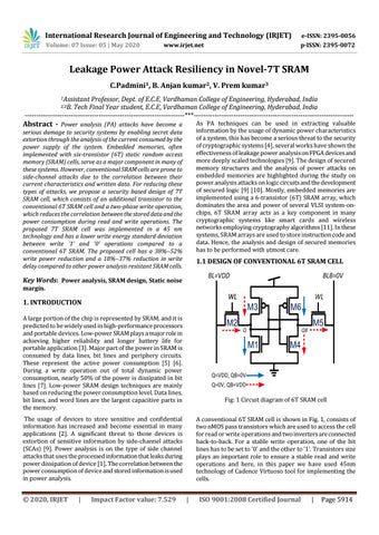
Fig: 1 Circuit diagram of 6T SRAM cell
The usage of devices to store sensitive and confidential information has increased and become essential in many applications [2]. A significant threat to those devices is extortion of sensitive information by side-channel attacks (SCAs) [9]. Power analysis is on the type of side channel attacks that uses the processed information that leaks during power dissipation of device [1]. The correlation between the power consumption of device and stored information is used in power analysis.
© 2020, IRJET
|
Impact Factor value: 7.529
A conventional 6T SRAM cell is shown in Fig. 1, consists of two nMOS pass transistors which are used to access the cell for read or write operations and two inverters are connected back-to-back. For a stable write operation, one of the bit lines has to be set to '0' and the other to '1'. Transistors size plays an important role to ensure a stable read and write operations and here, in this paper we have used 45nm technology of Cadence Virtuoso tool for implementing the cells.
|
ISO 9001:2008 Certified Journal
|
Page 5914