International Research Journal of Engineering and Technology (IRJET)
e-ISSN: 2395-0056
Volume: 07 Issue: 03 | Mar 2020
p-ISSN: 2395-0072
www.irjet.net
Green Electronics & Application of OFETs in Device Displays Ritika Chaudhary UG student, Dept. Of Electronics & Communication Engineering, Mahatma Gandhi Institute of Technology, Telangana, India ---------------------------------------------------------------------***---------------------------------------------------------------------2. OFET (ORGANIC FIELD-EFFECT TRANSISTOR) Abstract - The objective of this paper is to highlight the advancements in the domain of Green Electronics & Biodegradable Technology and design Bio-Compatible Display System using OFETs (Organic Field - Effect Transistors) . This technology proves to be crucial in the modern society as with the revolution in electronics, the necessity of eco-friendly materials in the design and manufacture of consumer products with display devices such as Smart Phones, Television, etc. are increasing in demand. Hence Non-Toxic & Sustainable components of natural origins are desired. Device Display is a current potential application area for sustainable component such as OFETs.. To reduce the number of contacts in displays and increase field contrast & selection ratio, introduction of elements such as transistors is highly desirable. Organic Field - Effect Transistors on plastic substrates including a mechanically flexible polymer dispersed liquid crystal display and displays containing e-Ink are used.
Transistors are the elementary foundation of any circuitry, and are used as switches or signal amplifiers. In field effect phenomenon the conductivity of a semiconductor changes due to the application of an electric field normal to its surface. The electric field is applied through a metallic gate in the device. OFETs are composed of three terminals i.e the source, drain, and gate, a semiconductor layer and an insulating layer between the semiconductor and gate. The OFET is similar to TFT (Thin-Film Transistor) in nature. A thin film deposited on a semiconductor, lies on nonconducting substrate.
Key Words: Green Electronics, Display, OFET, Transistor, Bio-compatible technology.
1. INTRODUCTION Green Electronics is the integration of electronics and environment friendly technology aimed at distinguishing the sustainable compounds which are of natural origin and non-toxic/biodegradable/bio-compatible. The main aim of this technology is to fabricate efficient substitute of synthetic compounds used extensively. "Green" electronics is oriented to deliver efficient energy consumption materials and low-cost devices and energy efficient materials and devices hence reducing E-waste.
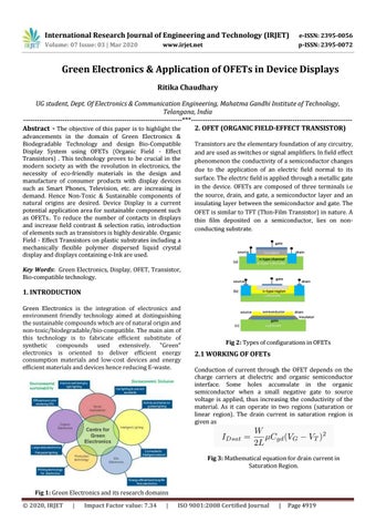
Fig 2: Types of configurations in OFETs
2.1 WORKING OF OFETs Conduction of current through the OFET depends on the charge carriers at dielectric and organic semiconductor interface. Some holes accumulate in the organic semiconductor when a small negative gate to source voltage is applied, thus increasing the conductivity of the material. As it can operate in two regions (saturation or linear region). The drain current in saturation region is given as
Fig 3: Mathematical equation for drain current in Saturation Region.
Fig 1: Green Electronics and its research domains Š 2020, IRJET
|
Impact Factor value: 7.34
|
ISO 9001:2008 Certified Journal
|
Page 4919