International Research Journal of Engineering and Technology (IRJET)
e-ISSN: 2395-0056
Volume: 06 Issue: 05 | May 2019
p-ISSN: 2395-0072
www.irjet.net
Design Verification of Universal Memory Controller IP Core (UMC) using System Verilog Architecture Jagadeesha Kolour1, Nagendra Reddy2, Venkata Siva Reddy3 1,2,3Dept.
of ECE Engineering, Reva University, Karnataka, Bangalore-India, 560064 ---------------------------------------------------------------------***----------------------------------------------------------------------
Abstract - An The word Design Verification itself tells that
having some specific function like, it has 8 chip select line and it support different types of memory. Single memory controller which is supporting different memories, for this UMC design, verification is done by generating a test cases in system Verilog language.
this paper does not involve Designing of Memory Controller Core, for the verification one needs its Design Specification Sheet to understand the working of the design so that it can be simulated in the Advanced Verification tools. The RTL logic is written in Verilog and the aim is verify every aspect of the design and to generate regression test cases in the Test-bench to obtain 100% Functional Coverage using System Verilog (SV). To understand Verification methodology first step is to understand about UMC IP Core specification and its role in as an intermediate Communication device which rest between memory & processor. MC commutes between the processor and memory accordingly as when the processor request for memory, each different type of memories connected at other end of MC has its own signals for communication which is taken care by the MC. Features of UMC includes SDRAM, SSRAM, FLASH, ROM and many other devices supported,8 Chip selects, each uniquely programmable, Flexible timing to accommodate a variety of memory devices, Burst transfers and burst termination, Supports RMW cycles, Performance optimization by leaving active rows open, Default boot sequence support, Dynamic bus sizing for reading from Async. Devices, Byte parity Generation and Checking, Multi Master Memory bus support, Industry standard WISHBONE SoC host interface, Up to 8 * 64 Mbyte memory size, Supports Power down Mode,
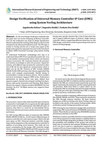
2. Universal Memory Controller F
Fig 1: Block diagram of UMC As can be seen in the above block diagram the processor communicates the UMC via wishbone interface and memories linked to the UMC are communicated respectively as per the signal required by the memories and the request generated via processor. Wish bone block is a place where we are verifying the UMC by checking read and write dada matching, if both read and write data matching then UMC is working properly and hence verification is done.
Key Words: UMC, DUT, WISHBONE, SDRAM, SSRAM, SYNC
Memory modules containing a different types of memory like SDRAM, SSRAM, and SYNC. These memories attached to the UMC through memory interface. All these memory designs are written in Verilog code, these Verilog codes are included in the top file of the system Verilog module. While verification system Verilog top modules are used.
1. INTRODUCTION The processor cannot really understand the type of memory connected to it and might not even generate the right signals need in order to fully communicate with different types of memory, thus there is a need for an intermediate device which seats between processor and the memories to handle such issues.
UMC is having its own architecture design with novel feature supporting. UMC is placed between WISHBONE and memory module. These blocks are interfaced by WISHBONE interface and memory interface to the UMC.
For SOC having different types of memories like SDRAM, DRAM, SSRAM, FLASH etc.., it will require different types of memory controllers for each memory types. Which will add extra space on SOC. Universal memory controller design, improved by integration of the existing memory controller in addition of providing novel features. This make the low power consumption for the design. UMC controller design which is supporting SDRM, SSRAM and SYNC memories what we call as Universal Memory Controller. This UMC design is
Š 2019, IRJET
|
Impact Factor value: 7.211
Wishbone is used as a portable interface in semiconductor IP cores whose purpose is to make system re-usability faster to overcome the Design integration problems. It also improves the portability and reliability of the system and results in faster time-to-market for the customer. Wishbone is not itself an IP core but is used as a specification required for the creation of IP core. It was created for the ease of interconnect interface understanding as well as for writing codes in HDL
|
ISO 9001:2008 Certified Journal
|
Page 1226