International Research Journal of Engineering and Technology (IRJET)
e-ISSN: 2395-0056
Volume: 06 Issue: 11 | Nov 2019
p-ISSN: 2395-0072
www.irjet.net
DESIGN OF ODD-EVEN PARITY GENERATOR USING SIX TRANSISTORS XOR-XNOR MODULE Abhishek Shukla 1, Subodh Wairya2 1M.Tech
scholar, I.E.T. , LUCKNOW I.E.T. , LUCKNOW ---------------------------------------------------------------------***---------------------------------------------------------------------2PROFESSOR,
Abstract -In the presented work we have used various XORXNOR modules to design the parity generator. Our main aim remains confined to the areas dealing with power, delay and power delay product. We have to design parity generator using various XOR-XNOR modules and compare their performance on the basis of above mentioned factors. The six transistors XOR-XNOR modules involved in the design of parity generator is basic fundamental unit simultaneously giving XOR-XNOR outputs. As we know that power and delay are inversely proportional quantities we will also calculate the power product delay. Simulations have been done on CADENCE VIRTUOSO software on 45nm Technology and all the simulations have been done at 27°C. Key Words: Parity Generator, CMOS Logic Gates, Power Delay Product Etc. 1. INTRODUCTION We know that in designing the electronic system today the one factor which is most concerned is that of energy consumption. Low energy consumption is needed for long durability of the energy supplying source such as for space applications where we need constant supply even for months or years.[10] Now as we have advanced various technologies have been evolved using CMOS logic, pass transistor logic, low power gates and many more. Now days to reduce the power consumption the testifying approach is to lower down the power supply but because of supply reduction there are various other anomalies which arise such as increase in delay functionality of the circuit vitiates.[7] So now a day while designing the electronic system our main aim remains to lower down the energy dissipation.
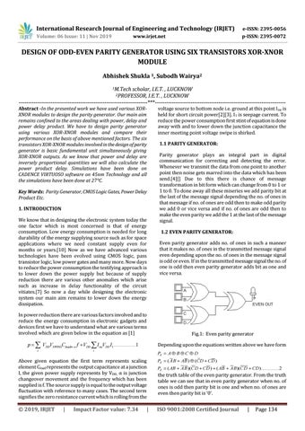
voltage source to bottom node i.e. ground at this point I isc is held for short circuit power[2][3]. I1 is seepage current. To reduce the power consumption first stint of equation is done away with and to lower down the junction capacitance the inner meeting point voltage swipe is shirked. 1.1 PARITY GENERATOR: Parity generator plays an integral part in digital communication for correcting and detecting the error. Whenever we transmit the data from one point to another point then noise gets marred into the data which has been send.[4][] Due to this there is chance of message transformation in bit form which can change from 0 to 1 or 1 to 0. To done away all these miseries we add parity bit at the last of the message signal depending the no. of ones in that message if no. of ones are odd then to make odd parity we add 0 or vice versa and if no. of ones are odd then to make the even parity we add the 1 at the last of the message signal. 1.2 EVEN PARITY GENERATOR: Even parity generator adds no. of ones in such a manner that it makes no. of ones in the transmitted message signal even depending upon the no. of ones in the message signal is odd or even. If in the transmitted message signal the no. of one is odd then even parity generator adds bit as one and vice versa.
In power reduction there are various factors involved and to reduce the energy consumption in electronic gadgets and devices first we have to understand what are various terms involved which are given below in the equation as [1]
Fig.1: Even parity generator
p VDDVSWINGCload f VDD I iscVDD I1..................1
Depending upon the equations written above we have form
i
i
Above given equation the first term represents scaling element Cload represents the output capacitance at a junction I, the given power supply represents by VDD, α is junction changeover movement and the frequency which has been supplied is f. The source supply is equal to the output voltage fluctuation with reference to many cases. The second term signifies the zero resistance current which is rolling from the
© 2019, IRJET
|
Impact Factor value: 7.34
|
PE A B C D PE ( A B AB ) (CD CD ) PE ( AB A B )(C D CD ) ( AB A B)(C D CD)...............2
the truth table of the even parity generator. From the truth table we can see that in even parity generator when no. of ones is odd then parity bit is one and when no. of ones are even then parity bit is ‘0’.
ISO 9001:2008 Certified Journal
|
Page 134