International Research Journal of Engineering and Technology (IRJET)
e-ISSN: 2395-0056
Volume: 06 Issue: 10 | Oct 2019
p-ISSN: 2395-0072
www.irjet.net
Implementation of Low Power 32-bit Carry-Look ahead Adder using Adiabatic Logic Muttappa Pujari1, Ashwini Desai2, Basavaraj C3 1PG
Student, Dept. of Electronics and Communication Engineering. Professor Dept. of Electronics and Communication Engineering. 3Assistant professor Dept. of Electronics and Communication Engineering. 123 KLE. Dr. M. S. Sheshgiri College of Engineering and Technology, Belagum-590008 Karnataka, India ------------------------------------------------------------------------***------------------------------------------------------------------------1.1 Conventional Logic Switching Abstract –Adiabatic logic is low power logic, in this 2Associate
paper an adiabatic logic based 32-bit carry look ahead adder is designed and implemented on the basis of efficient charge recovery logic (ECRL). Power dissipation of the proposed technique is compared with conventional CMOS circuit. The adiabatic (ECRL) shows less average power consumption than the conventional CMOS technique. The adder lies in the critical path of all the arithmetic operations so it plays a crucial role in determining the overall system performance. A schematic and simulation of proposed circuit is implemented in cadence virtuoso 6.1.5 using 45nm technology.
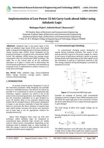
In conventional charging power dissipation is mainly during switching activities. The source of the pull-up network is given to the power supply VDD where as the source of pull-down network is given to ground. During steady state depending on the input signal one of the transistors in pull-up or pull-down network is ON. The energy required during discharging is provided by equations (1) to (4).
Key Words: ECRL adiabatic logic, Carry-Lookahead Adder, energy recovery, average power, cadence virtuoso, 45nm technology.
1. INTRODUCTION In present scenario power dissipation is one of the important parameter while designing any portable devices or embedded devices. The devices are said to be portable if it is minimized in terms of components like transistor, register, capacitor etc, which is one of the prime motto of present generation. According to Moore’s law the transistors embedded on IC gets doubled for every 18 months. Most of our customer demand long battery life for portable devices. If the power dissipation is larger in any devices, internally it heats the system. Hence to overcome the above situation it requires heat sink, which further increases the device size, therefore use of heat sink is not an appropriate solution for portable devices [2].
Figure -1: Conventional CMOS logic gate Consider an example of inverter with conventional charging as shown in figure1 here PMOS transistor turns ON when the input logic gate is low and hence if forms the direct path between VDD to output and load capacitor CL gets charged. The total charge Q taken from supply voltage can be given as 2 E C LVDD ..............1
During charging the energy stored in load capacitance is given by
Hence VLSI designers have come up with new technique called adiabatic logic. As compared to conventional logic, adiabatic logic circuits are widely used to reduce power consumption. Depending on the technique used in adiabatic logic i.e. either partially or fully, the energy is stored in load capacitor and can be recaptured back to power supply [5].
© 2019, IRJET
|
Impact Factor value: 7.34
Ech arg e
1 2 C L VDD ..........2 2
The NMOS transistor turns ON when the supply voltage is high. Hence it takes direct path from output to ground and whatever the charge is stored in load capacitance, it
|
ISO 9001:2008 Certified Journal
|
Page 1387