International Research Journal of Engineering and Technology (IRJET)
e-ISSN: 2395-0056
Volume: 04 Issue: 09 | Sep -2017
p-ISSN: 2395-0072
www.irjet.net
DESIGN AND SIMULATION OF A CMOS FUNCTION H. Abdul Wasay1 1Assistant
Professor, Dept. of Electronics and Communication Engineering, Deccan College of Engineering and Technology, Telangana State, India ---------------------------------------------------------------------***---------------------------------------------------------------------
Abstract – Implementing the function
using CMOS logic i.e. pull- up and pull- down combination and testing the implemented transistor based logical circuit using DSCH software aid. Key Words: DSCH software, pull- up and pull- down network, CMOS, NAND, NOR.
1. INTRODUCTION There are many transistor based functions which can be developed using CMOS logic. Significantly working with their design and accomplishing their switching performance via testing them using DSCH software, we able to study their working on all possible logical input combinations. Here I am implementing the function and testing it using DSCH software.
2. FUNDAMENTAL OF CMOS DESIGNING A CMOS function is fundamentally working on a basic combinational network of pull- up and pull- down network. The pull- up network is of pmos transistors and pull- down of nmos transistor combinations.
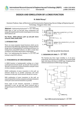
Fig.1. Pull- Up and Pull- Down Network
3. DESIGNING OF CMOS The function has three input variables i.e. A, B and C respectively. The function with a output F has A and B in NOR logic with along with them in NAND logic. Designing them with the fundamental of CMOS design topology.
NAND combination of pmos transistors in the pull- up network should be in parallel connection and nmos transistors in the pull- down network should be in series. NOR combination of pmos transistors in the pull- up network should be in series connection and nmos transistors in the pull- down network should be in parallel. Every input of the function represents a transistor separately in pull- up and pull- down network and is designed based on the NAND and NOR combination of CMOS logic.
Fig.2. CMOS circuit for the function
Š 2017, IRJET
|
Impact Factor value: 5.181
|
ISO 9001:2008 Certified Journal
| Page 1487