International Research Journal of Engineering and Technology (IRJET)
e-ISSN: 2395-0056
Volume: 04 Issue: 09 | Sep -2017
p-ISSN: 2395-0072
www.irjet.net
VHDL Implementation of High Speed and Low Power BIST Based Vedic Multiplier Manohar Mohanta1, P.S Indrani2 1Student,
Dept. of Electronics and Communication Engineering, MREC, Hyderabad, Telangana, India Professor, Dept. of Electronics and Communication Engineering, MREC, Hyderabad, Telangana, India ---------------------------------------------------------------------***--------------------------------------------------------------------2Asst.
Abstract - In modern electronics world applications of
integrated circuits are increasing day-to-day. All hardware segments which are produced are focusing on High speed, Low power and User agreeable application. Among these video and audio based processing applications are increasing. Multipliers are the essential consistent operational unit in any of the procedure. So we have outlined a high-speed multiplier utilizing our Indian customary multiplier called Vedic multiplier. Another vital equipment in testing modules is capacity to test the module independent from anyone else. The Built-in-selftest (BIST) feature encourages the user to verify the functionality and authenticate the module is defective or working fine. This paper presents a BIST based implementation of high-speed Vedic multiplier. The proposed design is realized by using Xilinx Tool using VHDL programming language. A low power Test Pattern Generator(TPG) used in design realization. Key Words: built-in-self-test, Pseudo Random Number Generator, Very Large Scale Integrated circuits, Very High Speed Integrated Circuit, Vedic Multiplier, Xilinx, VHDL.
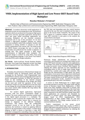
1. INTRODUCTION Nowadays, the performance of the hardware design can be evaluated using its operational speed and power consumed by the hardware. Field Programmable Gate Array(FPGA) is desired and promising high speed and low power consumption hardware. In FPGA the operation is based on the switching of the internal recourse architecture. For a development of the design, this FPGA can be used and verify the operation of the circuit architecture. If there are any modifications to be done, then we can change the circuit design and again we can verify. Low power system offers benefits like long battery life, high performance, etc. For modern digital applications, high-speed processor with low power consumption design is required. The most common and important module used in the digital signal processors is a multiplier. The multiplier is used to process the complex data. The selftesting feature is another feature that is required for testing or diagnosis of the different multiplier architecture. This feature helps the configurable integrated circuits to test by itself. In the self-test operation, the hardware is tested by applying different inputs for the functionality of the module. A simple block diagram of BIST is shown in Fig:1.Here a Logic BIST Controller is designed for controlling of the user data and
Š 2017, IRJET
|
Impact Factor value: 5.181
|
the TPG data and depending upon the control function selected by the user the mux is switched and the data is given to the Circuit Under Test(CUT). The output of the CUT is given to a response analyzer and the output of Logic BIST Controller is also given to the analysis the circuit which is developed.
Fig -1: Simple Block Diagram of BIST Design Numerous design adjustments are proposed by researchers and scientists are working with respect to low power BIST based rationale circuits for some applications. In this paper Low power test pattern generator designed by using Low-power Linear Feedback Shift Register. By utilizing this outline approach we have diminished the exchanging action in view of single input change design produced by a counter and a gray code converter. This design has the characteristics of high speed, low power consumption. A Low power Linear input move enlist based low power test design generator configuration is proposed. This paper mainly focuses on the BIST and how to reduce the power consumption. In this transition is reduced by generating the gray code with 1-bit distance. A review on Vedic Mathematics for a digital signal processing operation is present. This paper deals with the review of literature based Vedic Mathematics. A FPGA based 4-bit Vedic multiplier using LFSR is present. This document describes the implementation of the 4-bit Vedic multiplier enhances with the propagation delay. TPG is the major component of the BIST hardware design. Many BIST based applications are proposed and simulated by researches to propose power and speed optimization designs based on FPGA implementation. FPGA implementation of BIST enables UART for real time interface application. This design enables self-test of a common hardware interface. Today's requirement is low power circuit implementation of BIST Based logic circuits on FPGA to achieve high-speed operational circuits. The Test pattern is designed using a modified architecture by reducing the number of sequential circuits.
ISO 9001:2008 Certified Journal
| Page 799