
International Research Journal of Engineering and Technology (IRJET) e-ISSN: 2395-0056
Volume: 13 Issue: 06 | Jun 2026 www.irjet.net p-ISSN: 2395-0072
International Research Journal of Engineering and Technology (IRJET) e-ISSN: 2395-0056
Volume: 13 Issue: 06 | Jun 2026 www.irjet.net p-ISSN: 2395-0072
1Bhagyalakshmi Chinivalar, 2Dr M S Suma
1MTech Student, 2Professor, Dept of ECE,BMS College of Engineering, Bengaluru, India.
Abstract-This project presents the design and implementation of a 32-bit RISC-V processor integrated with a dedicated Floating-Point Coprocessor for high-performance floating-point computation. The core processor is based on the RV32I instruction set architecture, while the floatingpoint operations are offloaded to a separate IEEE-754 compliant Floating-Point Coprocessor, enabling efficient mixed-precision computing. The architecture employs a tightly coupled coprocessor interface that allows the main RISC-V core to dispatch floating-point instructions to the coprocessor and handle data exchange through dedicated registers and control signals. This modular approach provides better hardware separation, improved scalability, andeasier maintenancecomparedtoa unifiedexecutionunit. The design includes optimized modules for instruction fetch, decode, register file, integer ALU, control unit, hazard detection, and pipeline management in the main core, along with a complete floating-point coprocessor consisting of FPALU, floating-point register file, and coprocessor control logic. The entire system is implemented in Verilog HDL. It has been simulated, synthesized, and tested on an FPGA platform using the Vivado design suite. Pipeline hazards are effectively managed using forwarding, stalling, and hazard detection techniques to ensure smooth operation between the main processor and the floating-point coprocessor. Experimental results demonstrate significant performance gains in floating-point intensive workloads while maintaining low resource utilization on the FPGA. The proposed design offers an excellent balance between performance, flexibility, and hardware cost, making it highly suitable for embedded systems, IoT devices, signal processing, and other mixed integer-floating-pointapplications.
Keywords-RISC-V, Coprocessor, IEEE-754, Clock Gating, FPGA, Verilog HDL, Vivado.
The RISC-V architecture is an open-source Instruction Set Architecture (ISA) that is widely used in academics, research,andindustryduetoitsflexibility,simplicity,and free licensing model. Unlike traditional proprietary processor architectures, RISC-V allows designers to modify, extend, and optimize the processor based on application needs. This makes it an ideal platform for designing custom processors for embedded systems, digital signal processing, and machine learning applications. In this project, a RISC-V 5-stage pipelined processor is designed and implemented using Verilog HDL and synthesized on Xilinx Vivado. The five pipeline
stages Instruction Fetch (IF), Instruction Decode (ID), Execute (EX), Memory Access (MEM), and Write Back (WB) allow multiple instructions to be processed in parallel, improving overall performance. The final design isimplementedinVerilogHDLandtestedusingsimulation andsynthesisintheVivadodesignenvironment,makingit suitablefordeploymentonFPGAplatforms.Thisprocessor design demonstrates improved performance in applications involving real-time signal processing, data analysis, and embedded intelligent systems, while maintaining the modularity and openness of the RISC-V architecture.
A rigorous review of contemporary architectural exploration establishes the technical contextual baseline forthisstudy:
1) Banna Saif et al.: Implemented an FPGA-based educational RISC-V processor (RV32I) with a simple pipeline, emphasizing simplicity and hands-on learning forembeddedapplications.Thisaddressesaccessiblesoftcore configurations for basic controls but lacks singleprecisionnumericarithmeticaccelerationnetworks.
2) Saussereau et al.: ProposedAsteRISC,asize-optimized RISC-V core for design-space exploration, focusing on minimal area and efficient resource usage. The core focusesheavilyonoptimizingareafootprints,establishing structuralbenchmarksforresource-constrainedlayoutsat the cost of execution performance for data-intensive calculations.
3) Thanga Dharsni et al.: Presented a hazard-free pipelined RV32I RISC-V architecture, ensuring correct instruction execution without stalls for improved performance. Their techniques rely on optimized forwarding logic, minimizing structural bubbles across basicmathematicalworkflows.
4) Phangestu et al.: Implemented a five-stage pipelined 32-bit RISC-V soft processor in VHDL, supporting modular, FPGA-compatible educational and research applications, laying out classical instruction overlapping conventions.
5) Gupta et al.: Designed a high-speed, resource-efficient UART for reliable serial communication, suitable for peripheral integration with embedded processors like RISC-V, defining high-frequency clock divider methodologies.
International Research Journal of Engineering and Technology (IRJET) e-ISSN: 2395-0056
Volume: 13 Issue: 06 | Jun 2026 www.irjet.net p-ISSN: 2395-0072
RISC-V is an open-source Reduced Instruction Set Computing (RISC) instruction set architecture (ISA) that emphasizes simplicity, modularity, and extensibility. Developed at UC Berkeley, it is designed to support modern processor requirements while remaining straightforward enough for research, education, and customhardwaredevelopment. SimplicityandRegularity arepreservedviafixed-length32-bitinstructions(RV32I) whichmakeinstructiondecodingsimple,combinedwitha small set of general-purpose registers (32 registers × 32bit) for integer operations. It utilizes a Load/Store Architecture where only explicit load and store instructionsaccessmemory,whileallarithmeticandlogic operations operate exclusively on registers. Fixed instructionlengthandsimpleinstruction formatsmakeit ideal for pipelined implementations. RISC-V supports several instruction types, each optimized for a specific purpose: R-type (Register) for arithmetic/logic operations,I-type(Immediate)forarithmeticimmediates and loads, S-type for store configurations, B-type for conditionalbranches,U-typeforupperimmediates,andJtype for long jumps. Registers x0–x31 represent the 32 general-purposeregisters,wherex0ishardwiredtozero, x1(ra)servesasthereturnaddress,andx2(sp)operates asthestackpointer.
limitations whenappliedto modern real-worldworkloads. The absence of floating-point computation support restricts the processor to integer-only operations, making it unsuitable for applications involving signal processing, scientific computation, sensor data analysis, and control systems that inherently require floating-point arithmetic. Furthermore, implementing floating-point operations entirely in software on an integer-only core results in increased execution latency, higher power consumption, andreducedsystemthroughput.

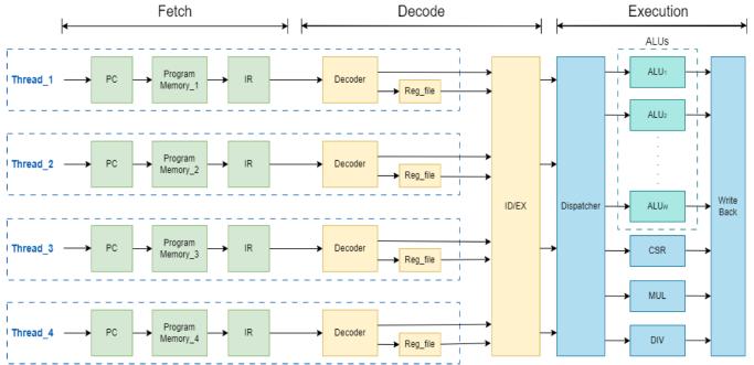
Fig. 2. Pipelined instruction sequencing and execution overlap mapping acrossthefivestructuralstages.


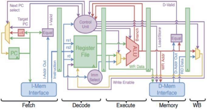
Fig. 1. Coresystemarchitecturalblockdiagramforthe baseline5-stage pipelinedintegerprocessor.
A pipeline architecture increases performance by executing multiple instructions simultaneously, each in different processing stages. The commonly used 5-stage pipeline (IF, ID, EX, MEM, WB) balances simplicity and performance. Research has shown that pipelining improves throughput without significantly increasing hardware complexity. However, pipelining also introduces challenges such as data hazards, control hazards, and structural hazards, which require hazard detection, stalling, and forwarding mechanisms to maintain correct execution. Although the existing 5-stage pipelined RISC-V processor based on the RV32I instruction set provides an efficient and resourceoptimized solution for integer-based embedded applications, it suffers from significant functional
A. Phase 1: Switchable Parallel Floating-Point Unit Architecture
Before achieving the final goals of implementing a floatingpointALUasanindependentcoprocessor,wefirst implemented a floating point ALU as a separate parallel block inside the same RISC-V processor in a switchable floating point methodology. This parallel arrangement ensured functional modularity, low hardware complexity, and seamless operation when floating-point capability is enabled.
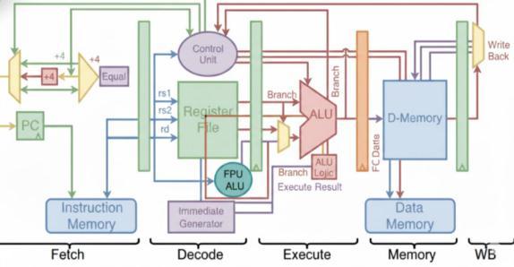
Fig. 3. Logical configuration of the 32-bit RISC-V pipeline with an integratedswitchableparallelFP-ALUexecution core.
The FP-ALU in this architecture supports the complete RV32F instruction set, including addition, subtraction, multiplication, division, floating-point to integer conversions,comparisons,andoptionalfusedmultiply-add operations. Internally, the FP-ALU is designed with IEEE754compliantdatapathsthatconsistofpre-normalization logic for operand alignment, multi-cycle arithmetic units
International Research Journal of Engineering and Technology (IRJET) e-ISSN: 2395-0056
Volume: 13 Issue: 06 | Jun 2026 www.irjet.net p-ISSN: 2395-0072
for multiplication and division, post-normalization stages for rounding, and exception-flag generation hardware. A multiplexer selects between the integer ALU output and the FP-ALU output in the Execute stage, allowing the Write Back stage to remain unchanged regardless of the operational mode of the FP unit. When floating-point support is disabled, the FP-ALU can be clock-gated or power-gated,reducingdynamicpowerconsumption.
B. Phase 2: Decoupled Floating-Point Coprocessor Topology
Toeliminatetheexecutionroutingoverheadofshared resource grids, a decoupled coprocessor model was developed. The proposed system integrates an efficient Floating-Point Unit (FPU) coprocessor with the main RISC-V processor. The main goal is to accelerate highprecision floating-point arithmetic operations while reducingtheworkloadonthemainRISC-Vcore,resulting insignificantlyimprovedoverallsystemperformance.
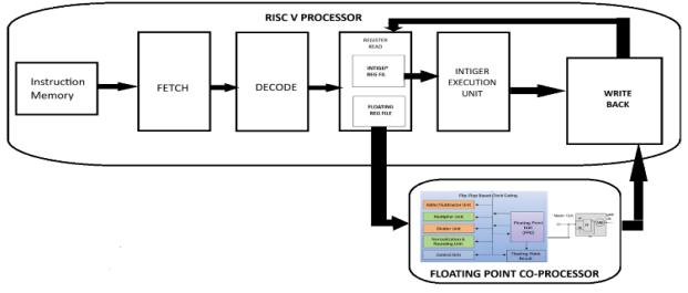
Fig. 4. Interconnecttopologyandisolatedstructural domainmappingofthe Floating-PointCoprocessor system
In this design, switching between execution units is performed cleanly via hardware opcode parsing in the Decode stage. Main integer instructions (OP=0110011, OP-IMM=0010011) route down the host pipeline, while floating-point paths (OP-FP=1010011, LOADFP=0000111, STORE-FP=0100111) are dispatched across the handshakeinterface.
x_issue_valid and x_issue_ready alongside instruction tokens, whereas signals from FPU to Core encompass x_result_valid, x_result_ready, output data, and updated exceptionflags.Thishandshakesupportenablesdecoupled execution, allowing the FPU to operate ahead of the main pipelinewhentherearenodatadependencies.
The design incorporates flip-flop-based clock gating to reduce power consumption. When a functional unit is not in use, its clock signal is disabled, preventing unnecessary switching activity and lowering dynamic power usage. It usesacombinationofaflip-flopandlogicgatestogenerate a glitch-freegatedclock.Theenablesignal issynchronized with the system clock using a negative-edge flip-flop. The gatedclock is then selectively distributed to modules such astheadder,multiplier,andregisters.Onlyactivemodules receive the clock signal at any time, which significantly improves energy efficiency, especially in applications wherefloating-pointoperationsareusedintermittently.
Comprehensive layout implementation, physical synthesis, and dynamic power estimation were conducted withinXilinxVivadotocapturethestrictoperationallimits ofthethreeprocessingparadigms.
The layout synthesis waveforms and physical reports fortheparallelintegrateddesignaredetailedbelow.Dueto routing resource competition within the unified Execution block, significant signal propagation overheads are observed.
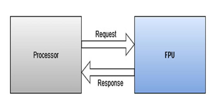

Fig. 5. Commandissueandresponsevalidation handshakeboundary protocol(X-IFInterface).
Modern RISC-V designs use a standardized Coprocessor eXtension Interface (X-IF) for clean integration. The signals from Core to FPU comprise
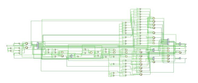
Fig. 6. Synthesized RTL schematic plot for the parallel switchable FPU systemlayout.
International Research Journal of Engineering and Technology (IRJET) e-ISSN: 2395-0056
Volume: 13 Issue: 06 | Jun 2026 www.irjet.net p-ISSN: 2395-0072
Vivado Utilization Sheet Fragment:
riscv_core:2146LUTs,391Registers,1F7Mux,0.5 BRAM,3 DSPs
└─ EX_STAGE:1172LUTs,0Reg,3DSPs
└─ ID_STAGE:83LUTs,0Reg
└─
└─
IF_STAGE:144LUTs,57Reg
WB_STAGE:746LUTs,0Reg,1F7Mux

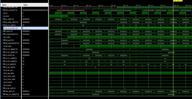
Fig. 7 Verification timing waveforms for instruction parsing under the parallelswitchabledesign.

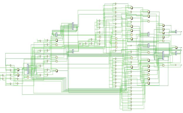
Fig. 11. Synthesized RTL schematic plot for the decoupled coprocessor systemsetup.
Vivado Critical Timing Paths:
Path 1: idex_rs1_addr_reg[0]/C → exmem_alu_result_reg[0]/ D | Total Delay: 82.577 ns (Logic: 59.519 ns)
Path 2: idex_rs1_addr_reg[1]/C → exmem_alu_result_reg[1]/ D | Total Delay: 79.533 ns (Logic: 57.457 ns)
Path 3: idex_rs1_addr_reg[2]/C → exmem_alu_result_reg[2]/ D | Total Delay: 77.123 ns
Fig. 8. FPGAAreautilizationlogsheetfortheintegrated parallelswitchable FPUconfiguration.
Vivado Power Analysis Summary:
TotalOn-ChipPower:94.508W(Junctiontemp exceeded!) Dynamic:93.467 W(99%)
└─ Signals:22.506W|Logic:29.862W| BRAM:0.134W| DSP:1.844 W| I/O:39.121
Junction Temperature: 125.0°C

Fig. 9 Synthesized total power dissipation spectrum for the parallel switchablebaselinelayout.

Vivado Critical Timing Paths:
Path 1: idex_rs1_addr_reg[0]/C → exmem_alu_result_reg[0]/ D | Total Delay: 82.577 ns (Logic: 59.519 ns)
Path 2: idex_rs1_addr_reg[1]/C → exmem_alu_result_reg[1]/ D | Total Delay: 79.533 ns (Logic: 57.457 ns)
Path 3: idex_rs1_addr_reg[2]/C → exmem_alu_result_reg[2]/ D | Total Delay: 77.123 ns (Logic: 55.656 ns)
Fig. 10. Propagation delay critical-path report tracking within the parallel switchableexecutionunit.
B. Paradigm II: Decoupled Floating-Point Coprocessor Reports
By moving the hardware blocks onto an independent coprocessor extension bus, the shared integer execute multiplexers are bypassed. The corresponding structural schematicsandhardwarereportsarepresentedbelow.
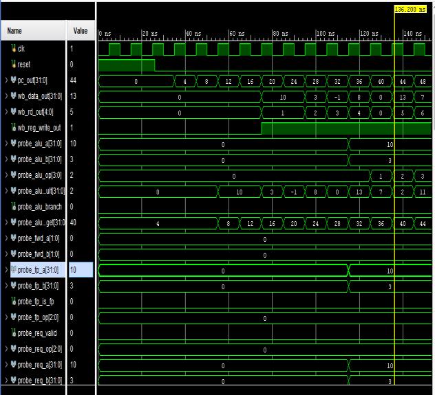
Fig. 12. Handshakecontrolvalidationwaveformsfor decoupledcoprocessor buscycles.

Vivado Area Sheet Fragment (Decoupled): riscv_core_with_ext_fpu:4308LUTs,732Registers, 8F7 Muxes,0.5 BRAM,2 DSPs
└─ EX_STAGE:472LUTs,0Reg,1F7Mux
└─ EXT_FPU:3540LUTs, 177Reg,7F7Muxes,2 DSPs
└─ FPU_INTF:14LUTs,37Reg
Fig.13. FPGA Area utilization report for the un-gated decoupled coprocessorarchitecture

Vivado Timing Sheet Fragment (Decoupled Loop): Path 1: exmem_rd_addr_reg[3]/C → EXT_FPU/ fpu_result_reg[0]/D | Delay: 73.309 ns (Logic: 36.34 ns) Path 2: exmem_rd_addr_reg[3]/C → EXT_FPU/ fpu_result_reg[1]/D | Delay: 70.357 ns (Logic: 34.81 ns) Path 3: exmem_rd_addr_reg[3]/C → EXT_FPU/ fpu_result_reg[2]/D | Delay: 67.330 ns (Logic: 33.28 ns) ns
Fig. 14. Critical path timing analysis summary sheet for the decoupled coprocessorloop.
International Research Journal of Engineering and Technology (IRJET) e-ISSN: 2395-0056
Volume: 13 Issue: 06 | Jun 2026 www.irjet.net p-ISSN: 2395-0072
Vivado Optimized Power Summary (Gated Decoupled):
Total On-Chip Power: 0.157 W
Dynamic Power: 0.052 W (33%) | Static Standby: 0.105 W (67%)
Dynamic Breakdown Signals: 0.022 W | Logic: 0.023 W
| BRAM: 0.000 W | DSP: 0.000 W | I/O: 0.007 W

Junction Temperature: 26.8°C | Thermal Margin: Fig. 15. Total power estimation metrics sheet for the decoupled un-gated coprocessornetlist.
C. Paradigm III: Clock-Gated Decoupled Coprocessor Reports
Integrating negative-edge D-type flip-flop synchronizationpathslimitsclocktreetogglingstrictlyto mathematically active modules, drastically cutting dynamic power. The physical layout, timing safety waveforms,andpowerreportsaregivenbelow.
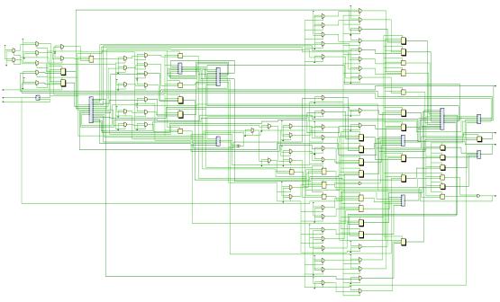
Fig. 16. Synthesized RTL schematic for the finegrained clock-gated coprocessorlayout.
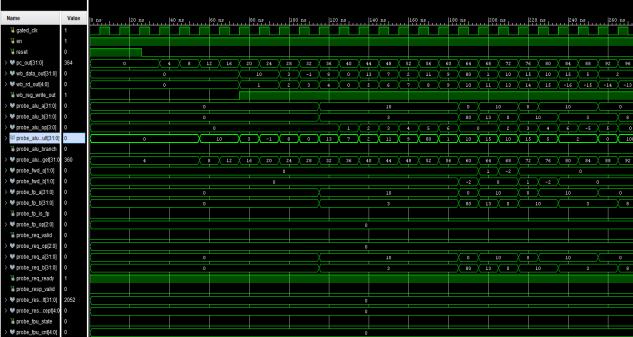
17. Simulation waveforms tracking clock disabling cycles during arithmeticidlephases.
Vivado Area Allocation Sheet (Gated Coprocessor):
riscv_core_with_ext_fpu_E:4309LUTs,733 Registers,8F7
Muxes,0.5 BRAM,2DSPs,2 BUFGCTRL
└─ EXT_FPU:3540LUTs,177Registers,2DSPs
└─ f10(Flipflop_CG):0LUTs, 1Register
Fig. 18 FPGA Area utilization sheet for the proposed clock-gated coprocessorcore.

Vivado Post-Synthesis Timing Summary (Gated): Path 1: exmem_rd_addr_reg[3]/C →
EXT_FPU/ fpu_result_reg[0]/D | Total Delay: 73.309 ns Path 2: exmem_rd_addr_reg[3]/C → EXT_FPU/ fpu_result_reg[1]/D | Total Delay: 70.357 ns Path 9: exmem_rd_addr_reg[3]/C → EXT_FPU/ fpu_result_reg[8]/D | Total Delay: 48.994
Fig. 19. Post-synthesis timing slack and propagation delay report for the gatedcoprocessor.
Vivado Power Summary (Decoupled Un-gated): TotalOn-ChipPower:33.057W(Junctiontemp exceeded) Dynamic:32.017 W(97%) └─ Signals:6.898W|Logic:7.448W|BRAM: 0.127W| DSP:1.890 W |I/O:15.654 W

Fig. 20. Optimizedpowerestimationspectrumforthe proposedclock-gated decoupledconfiguration.
D. Consolidated Comparative Analysis
The exact resource parameters extracted from the VivadolayoutengineareconsolidatedinTableIandTable II, providing a clear comparison of the physical design spaces.
TABLE I FPGARESOURCEALLOCATIONMETRICSACROSS MODULES
(Execute Block)
International Research Journal of Engineering and Technology (IRJET) e-ISSN: 2395-0056
Volume: 13 Issue: 06 | Jun 2026 www.irjet.net
TABLE II SYNTHESIZEDON-CHIPPOWERANDTHERMAL PERFORMANCE COMPARISON
32-bit RISC-V processing system featuring an independent IEEE-754 single-precision floating-point coprocessor. By offloading heavy math routines via an opcode-driven hardware routing mechanism, the architecture improves timing safety and eliminates the high execution latencies caused by software-based floating-point emulation. The integration of a glitch-free, flip-flop-based fine-grained clock gating framework provides an exceptional powersaving profile. It restricts clock tree switching to actively computing modules while preserving a compact logic footprint on the target FPGA. The proposed architecture achievesa99.83%dropinactiveon-chippowerdissipation and cuts critical path propagation delay by 11.22% compared to standard integrated alternatives, presenting an ideal framework for low-power edge platforms, IoT nodes, embedded signal processing, and real-time intelligentcontrolsystems.
[1]D. A. Patterson and J. L. Hennessy, Computer Organization and Design: The Hardware/Software Interface,5thed.,MorganKaufmann,2014.
[2]A. Waterman and K. Asanović, The RISC-V Instruction Set Manual - Volume I: User-Level ISA, Version 2.2, RISC-VFoundation,2019.
[3]RISC-V International, The RISC-V Privileged ArchitectureSpecification, Version1.12,2021.
[4]IEEEStandardsAssociation,IEEEStandardforFloatingPoint Arithmetic,IEEEStd754-2008.
[5]J. L. Hennessy and D. A. Patterson, "A New Golden Age for Computer Architecture," Communications of the ACM,vol.62,no.2,pp.48-60, Feb.2019.
[6]S.B.Furber,ARMSystem-on-ChipArchitecture,2nded., Addison-Wesley,2000.
The comparative findings confirm that the baseline integrateddesign(ArchitectureI)exhibitsextremepower dissipation (94.508 W) and hits a critical thermal ceiling of 125.0°C. Moving to a decoupled coprocessor model (Architecture II) isolates the execution nodes, dropping totalpowerto33.057W.Theintroductionoffine-grained clock gating (Architecture III) achieves a major breakthrough,loweringtotalon-chippowerconsumption tojust0.157W a99.83%powerreductioncomparedto the baseline system, while stabilizing the junction temperature at a cool 26.8°C. Critical path timing is simultaneously optimized by 11.22% (falling from 82.577 ns to 73.309 ns) due to the removal of long selection multiplexer paths within the core's Executestage.
This paper successfully presents the design, software verification,andsynthesisoptimizationofapower-aware
[7]D. Patterson, "Reduced Instruction Set Computers," Communications of the ACM, vol. 28, no. 1, pp. 8-21, Jan.1985.
[8]K. Asanović et al., "The RISC-V Instruction Set Manual," University of California, Berkeley, Tech. Rep. UCB/EECS-2014-54,2014.
[9]P.MishraandN.Dutt,ProcessorDesign:System-on-Chip Computing for ASICs and FPGAs, Morgan Kaufmann, 2007.
[10] S. Kilts, Advanced FPGA Design: Architecture, Implementation, and Optimization, Wiley-IEEE Press, 2007.