
International Research Journal of Engineering and Technology (IRJET) e-ISSN: 2395-0056
Volume: 13 Issue: 04 | Apr 2026 www.irjet.net p-ISSN: 2395-0072
International Research Journal of Engineering and Technology (IRJET) e-ISSN: 2395-0056
Volume: 13 Issue: 04 | Apr 2026 www.irjet.net p-ISSN: 2395-0072
Mrs.S. Jeyaseeli1 , K. Kaviya2
1Assistant Professor, Dept of EEE, VV College of Engineering, Tamilnadu, India
2Student, Dept of EEE, VV College of Engineering, Tamilnadu, India
Abstract - Multilevel inverters (MLIs) play an important role in modern power electronic systems due to their abilityto generate high-quality output voltage with reduced harmonic distortion. Among the different configurations, the three-level diode clamped multilevel inverter (DCMLI), flying capacitor multilevel inverter (FCMLI), and cascaded H-bridge multilevel inverter (CHBMLI) are widely used in various applications such as renewable energy systems and motor drives. This paper presents a comparative analysis of these three threelevel multilevel inverter topologies using MATLAB/Simulink. The comparison is carried out based on total harmonic distortion (THD), which is a key parameter used to evaluate the quality of the output voltage waveform. Each inverter topology is modeled and simulated under similar operating conditions to ensure accurate performance comparison. The output voltage waveforms and harmonicspectraare analyzed using FFT analysis in MATLAB/Simulink. The simulation results demonstrate the differences in harmonic performance among the three inverter topologies. The study provides insights into selecting the most suitable three-level multilevel inverter topology for applications requiring improved power quality and reduced harmonic distortion.
Multilevel inverters (MLIs) have become an important technologyinmodernpowerelectronicsystemsduetotheir abilitytoproducehigh-qualityoutputvoltagewithreduced harmonic distortion. Conventional two-level inverters generateoutputvoltageswithlargeharmoniccomponents, which may lead to increased switching losses, electromagnetic interference, and reduced efficiency in electricalsystems.Toovercometheselimitations,multilevel invertertopologieshavebeendevelopedtoproducestepped voltage waveforms that closely approximate a sinusoidal waveform. Among the different multilevel inverter configurations, the diode clamped multilevel inverter (DCMLI),flyingcapacitormultilevelinverter(FCMLI),and cascaded H-bridge multilevel inverter (CHBMLI) are the mostcommonlyusedtopologies.Theseinvertersgenerate multiple voltage levels by using power semiconductor switches,capacitors,andDCvoltagesources.Byincreasing thenumberofvoltagelevels,theoutputwaveformquality improves and the harmonic distortion decreases significantly. In power electronic systems, harmonic distortion is a critical factor that affects the overall performanceofelectricalequipment.Excessiveharmonics
cancauseadditionalpowerlosses,overheatingofdevices, and poor power quality. Therefore, Total Harmonic Distortion(THD)iswidelyusedasanimportantparameter to evaluate the performance of inverter topologies. This paperpresentsacomparativestudyofthree-levelmultilevel inverter topologies, including diode clamped, flying capacitor,andcascadedH-bridgeinverters.Thecomparison iscarriedoutusingMATLAB/Simulinksimulationmodels. Eachinverterisdesignedundersimilaroperatingconditions toensureanaccuratecomparison.Theperformanceofthe invertersisanalyzedbasedontheTotalHarmonicDistortion (THD)oftheoutputvoltagewaveform.Theobjectiveofthis studyistoanalyzeandcomparetheharmonicperformance of these three inverter topologies and identify the most suitableconfigurationforapplicationsrequiringimproved powerqualityandreducedharmonicdistortion.
Theadvancementofmultilevelinverter(MLI)technologyhas gained considerable interest in contemporary power electronics because of its capability to produce superior outputvoltagewithlowerharmonicdistortionandenhanced overall power quality. Various research studies have investigateddifferentmultilevelinvertertopologiesandtheir performancecharacteristics,particularlyfocusingonDiodeClamped Multilevel Inverter (DCMLI), Flying Capacitor Multilevel Inverter (FCMLI), and Cascaded H-Bridge MultilevelInverter(CHBMLI).
Acomparativestudypresentedin[1]analyzesthese three inverterconfigurationsbasedonparameterssuchascircuit structure, number of switching devices, output voltage waveform,andharmonicdistortioncharacteristics.Thestudy explains that multilevel inverters produce stepped output voltage waveforms that closely approximate sinusoidal waveforms, thereby reducing harmonic components and improving the overall efficiency of the power system. The results also indicate that the cascaded H-bridge inverter providesbetterharmonicperformanceandmodularitydueto its independent DC sources and flexible configuration. Anotherstudyin[2]highlightstheimportanceofPulseWidth Modulation(PWM)techniquesincontrollingtheswitching operations of inverterdevices. PWM methods,particularly multicarrier PWM techniques, help reduce harmonic distortion and improve the quality of the output voltage waveform.TheperformancecomparisonofCHB,NPC,andFC
International Research Journal of Engineering and Technology (IRJET) e-ISSN: 2395-0056
Volume: 13 Issue: 04 | Apr 2026 www.irjet.net p-ISSN: 2395-0072
inverter topologies under PWM control shows that the cascaded H-bridge inverter generally produces lower harmonicdistortionandimprovedvoltagewaveformquality compared to the other topologies. A simulation-based investigation reported in [3] analyzes multilevel inverter topologiesusingMATLAB/Simulink,wherediode-clamped, flying capacitor, and cascaded H-bridge inverters are modeledandevaluatedintermsofoutputvoltagewaveform, switching behavior, and Total Harmonic Distortion (THD). The harmonic spectrum of the inverter output voltage is obtained using Fast Fourier Transform (FFT) analysis, demonstratingthatmultilevelinverterssignificantlyreduce harmonic distortion compared to conventional inverters, while the cascaded H-bridge topology shows improved performance due to its modular structure and reduced switchinglosses.
Furtheranalysispresentedin[4]explainsthestructuraland operationaldifferencesamongmultilevelinvertertopologies. The diode-clampedinverterusesclampingdiodesandDCbus capacitors to generate multiple voltage levels, which makesitsuitableforhigh-voltageapplicationsbutincreases circuitcomplexityasthenumberofvoltagelevelsincreases. Theflyingcapacitorinverteremploysfloatingcapacitorsto produce intermediate voltage levelsand offersadvantages suchasvoltagebalancingcapabilityandredundantswitching states, although it requires a large number of capacitors, increasing system cost and complexity. In contrast, the cascadedH-bridgeinverterconsistsofmultipleH-bridgecells connectedinseries,eachsuppliedbyseparateDCsources, whichprovidesamodularstructureandscalabilityforhigher voltagelevels.Researchfocusingonharmonicperformancein [5] analyzes how different multilevel inverter topologies influence harmonic distortion levels in the output voltage waveform. Harmonics in power systems can lead to additionalpowerlosses,overheatingofelectricalequipment, and reduced system efficiency. Therefore, minimizing harmonic distortion is an important objective in inverter design, and increasing the number of voltage levels significantlyimproveswaveformquality.
Anotherstudyin[6]explainsthe use ofFFTtechniquesto analyzeharmoniccomponentsininverteroutputwaveforms. FFT converts time-domain signals into frequency-domain representations,allowingaccurateidentificationofharmonic frequencies. The performance of multilevel inverters is commonlyevaluatedusingTotalHarmonicDistortion(THD), which measures the ratio of harmonic components to the fundamentalcomponentofthewaveform.
Adetailedreviewpresentedin[7]describesthe operating principlesofthediode-clampedinverter,alsoknownasthe Neutral Point Clamped (NPC) inverter, where the DC bus voltageisdividedintomultiplelevelsusingcapacitorsand clampingdiodes.Thisconfigurationreducesvoltagestresson switchingdevicesandimproveswaveformquality,although voltage balancing becomes challenging at higher levels.
Another study in [8] investigates the simulation of the cascaded H-bridge multilevel inverter using MATLAB/Simulink and demonstrates that this topology produces stepped output voltage waveforms with lower harmonicdistortioncomparedtoconventionalinverters.The modularstructureofthecascadedH-bridgeinverterenables easyexpansiontohighervoltagelevelsandmakesitsuitable for renewable energy integration, industrial power converters, and motor drives. Furthermore, research presented in [9] discusses the design and simulation of a three-level multilevel inverter for power electronic applications, where the results indicate improved output voltagewaveformquality,reducedharmonicdistortion,and lower switching stress on power devices. Overall, the reviewed literature indicates that multilevel inverter technology plays a significant role in improving power quality in modern power electronic systems. Among the different inverter configurations, the cascaded H-bridge multilevel inverter is often considered the most advantageousduetoitsmodularstructure,lowerharmonic distortion, and flexibility in generating multiple voltage levels.Thesecharacteristicsmakemultilevelinvertershighly suitableforapplicationssuchas renewable energysystems, motor drives, electric vehicles,and high-power industrial powerconversionsystems.
Amultilevelinverter(MLI)isapowerelectronicdevicethat convertsdirectcurrent(DC)intoalternatingcurrent(AC)by producingmultiplevoltagelevelsattheoutputinsteadofjust twolevelsasinconventionalinverters.Bygeneratingseveral steppedvoltagelevels,theoutputwaveformbecomescloser toasinusoidalwaveform,whichhelpsinreducingharmonic distortionandimprovingpowerquality.Multilevelinverters are widely used in medium- and high-power applications such as renewable energy systems, motor drives, electric vehicles,andindustrialpowerconvertersbecausetheyoffer advantages like lower switching losses, reduced electromagneticinterference,andimprovedefficiency.The maintypesofmultilevelinvertertopologiesincludediodeclamped (neutral point clamped), flying capacitor, and cascaded H-bridge inverters, each having different circuit structuresandoperationalcharacteristics.Amongthese,the cascaded H-bridge inverter is often preferred due to its modularstructure,lowerharmonicdistortion,andflexibility in generating multiple voltage levels. Overall, multilevel inverters play a crucial role in modern power electronic systemsbyprovidinghigh-qualityACoutputwithreduced harmonicsandenhancedsystemperformance.
Fig.2.1illustratesthebasicstructureofathree-leveldiodeclampedmultilevelinverter,alsoknownasaNeutralPoint Clamped(NPC)inverter.Inthisconfiguration,theDCinput
International Research Journal of Engineering and Technology (IRJET) e-ISSN: 2395-0056
Volume: 13 Issue: 04 | Apr 2026 www.irjet.net p-ISSN: 2395-0072
voltage isdividedintotwoequalvoltagelevelsusingtwo capacitors and ,whichcreateaneutralmidpointinthe circuit. The inverter legconsists of four switching devices and ,whichcontrolthegenerationoftheoutput voltagesuppliedtotheload.Additionally,clampingdiodes and areusedtoconnectthemidpointofthecapacitors totheswitchingnodes,ensuringthatthevoltageacrosseach switch is limited and properly balanced. By operating the switchesindifferentcombinations,theinvertercanproduce threedistinctoutputvoltagelevels: , ,and These stepped voltage levels help generate an output waveform that closely resembles a sinusoidal waveform, therebyreducingharmonicdistortionandimprovingpower quality. Due to these advantages, the three-level diodeclampedinverteriswidelyusedinmedium-andhigh-power applications such as motor drives, renewable energy systems,andindustrialpowerconversionsystems.
alsohelpsmaintainvoltagebalancingandprovidesmultiple switching combinations to achieve the same output level, whichimprovestheflexibilityofcontrol.Duetothestepped output waveform produced by this inverter, harmonic distortionisreducedandtheoutputvoltagebecomescloser to a sinusoidal waveform, resulting in improved power quality.Therefore,theflyingcapacitormultilevelinverteris widelyusedinhigh-powerapplicationssuchasmotordrives andindustrialpowerconversionsystems.
2.2
Fig.2.2showsthecircuitconfigurationofathree-levelFlying CapacitorMultilevelInverter(FCMLI).Inthistopology,the DCinputvoltageisconvertedintoACusingmultiplepower semiconductorswitches(S1,S2,S3,andS4)alongwithflying capacitors that help generate intermediate voltage levels. The flying capacitor is connected between the switching nodesand actsasan energy storage element thatcharges and discharges during switching operations. Unlike the diode-clampedinverter,thistopologydoesnotuseclamping diodes;instead,itusescapacitorstomaintaintherequired voltage levels. By controlling the switching states of the inverter switches, the circuit can generate three output voltagelevels:+Vdc/2,0,and−Vdc/2.Theflyingcapacitor
Fig.2.3showsthebasicH-Bridgeinvertercircuit,whichis thefundamentalbuildingblockusedinaCascadedH-Bridge Multilevel Inverter (CHBMLI). The circuit consists of four powersemiconductorswitches(S1,S2,S3,andS4)arranged inanH-shapedconfiguration,alongwithaDCvoltagesource (Vdc)andaloadconnectedbetweenthemidpointofthetwo switchlegs.TheoperationoftheH-bridgeinverterisbased oncontrollingtheswitchingstatesofthesefourswitchesto generatedifferentvoltagepolaritiesacrosstheload.When switchesS1andS4areturnedONwhileS2andS3areOFF, theloadreceivesapositivevoltage(+Vdc).Whenswitches S2 and S3 are turned ON while S1 and S4 are OFF, the polarity across the load reverses and the output becomes Vdc. If switches S1 and S2 or S3 and S4 are turned ON simultaneously,theoutputvoltageacrosstheloadbecomes zero.
International Research Journal of Engineering and Technology (IRJET) e-ISSN: 2395-0056
Volume: 13 Issue: 04 | Apr 2026 www.irjet.net p-ISSN: 2395-0072
-3
InaCascadedH-BridgeMultilevelInverter,multipleH-bridge cellsliketheoneshowninthefigureareconnectedinseries, each supplied by a separate DC source. By combining the output voltages of several H-bridge cells, the inverter can generate multiple stepped voltage levels such as +Vdc, +Vdc/2,0,−Vdc/2,and−Vdc,dependingonthe numberof cells used. This stepped waveform closely approximates a sinusoidalwaveform,whichsignificantlyreducesharmonic distortion and improves power quality. The modular structureofthecascadedH-bridgeinvertermakesiteasyto increasethenumberofvoltagelevelsbysimplyaddingmore H-bridgecells,whichiswhythistopologyiswidelyusedin motordrives.
The figure 4 illustrates the MATLAB/Simulink model of a three-leveldiode-clampedmultilevelinverter(DCMLI)along withitscontrolcircuitryandoutputmeasurementsystem. The left section of the model represents the control signal generation unit, where a sine wave acts as the reference signalforgeneratingthedesiredACoutput.Tworepeating sequenceblocksareusedtogeneratecarriersignalsforpulse widthmodulation(PWM).Thesesignalsarecomparedusing relational operator blocks, which determine the switching conditions by comparing the reference and carrier waveforms. The logical outputs from the comparators are processed using logical operator blocks to produce gate signals (s1, s2, s3, and s4). These signals are transmitted through Goto and from blocks to control the switching devices in the inverter circuit. The power Gui block is includedtoconfigurethesimulationenvironmentandenable the analysis of power electronic components within the MATLAB/Simulinkplatform.
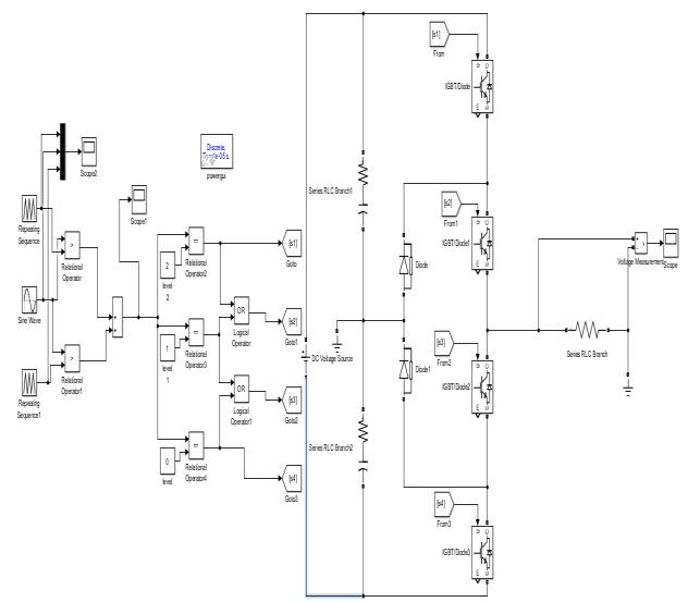
Therightsectionofthemodelrepresentsthepowercircuit of the diode-clamped multilevel inverter and the load system. A DC voltage source provides the input supply, whichisdividedusingcapacitivebranchestocreatemultiple voltagelevels.TheinverterconsistsoffourIGBTswitches withanti-paralleldiodes,whicharecontrolledbythegate signals generated in the control circuit. Additionally, clampingdiodesareusedtomaintainvoltagebalanceacross theswitchesandtogeneratetheintermediatevoltagelevel requiredforthree-leveloperation.Byproperlycontrolling the switching states of the IGBTs, the inverter produces three output voltage levels (+Vdc/2, 0, and −Vdc/2). The outputisconnectedtoaseriesRLCbranchrepresentingthe load,andavoltagemeasurementblockisusedtomonitor theoutputwaveformthroughascope.Thissimulationmodel demonstrates how a three-level diode-clamped multilevel inverter converts DC input into a stepped AC output with reduced harmonic distortion, thereby improving overall powerquality.
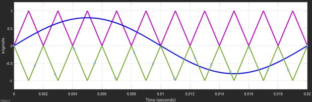
Fig -5:ReferenceandcarriersignalsusedinthePWM switchingscheme.
Thefigure5showsthecomparisonbetweenthereference sinewaveandthecarriertriangularsignalsusedforPulse WidthModulation(PWM)inthemultilevelinvertercontrol system. The blue waveform represents the sinusoidal referencesignal,whichcorrespondstothedesiredACoutput waveformoftheinverter.Themagentaandgreentriangular
International
Volume: 13 Issue: 04 | Apr 2026 www.irjet.net p-ISSN: 2395-0072
waveforms represent the carrier signals that are used for generatingswitchingpulses.Thiscarriersignalsoperateata higherfrequencycomparedtothereferencesinewave.By comparingthereferencesignalwiththecarriersignalsusing relationaloperatorsinthecontrolcircuit,switchingpulses are generated to control the inverter switches. When the reference signal is greater than the carrier signal, the switchingdeviceturnsON,andwhenitislower,thedevice turnsOFF.Thiscomparisonprocessformsthebasisofthe PWM technique, which allows the inverter to produce a stepped output voltage that closely approximates a sinusoidalwaveform.Asaresult,theharmonicdistortionin theoutputvoltageisreducedandtheoverallpowerquality ofthemultilevelinvertersystemisimproved.
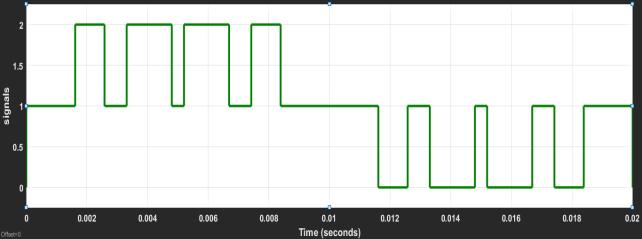
Thefigure6showstheswitchingsignalwaveformobtained fromtheoutputscopeoftheMATLAB/Simulinkmodelused to control the multilevel inverter. The horizontal axis representstimeinseconds,whiletheverticalaxisrepresents the logic level of the switching signal generated by the controlcircuit.Thesesignalsareproducedthroughthepulse width modulation (PWM) technique, where the reference sinewaveiscomparedwithcarriersignalsusingrelational andlogicaloperatorstogenerategatepulses.Thewaveform indicates the ON and OFF states of the inverter switches, wherehigherlogiclevelsrepresenttheswitchingdevicesin theONstateandlowerlevelsrepresenttheOFFstate.These switching pulses are applied to the IGBT switches in the inverter circuit, allowing the inverter to generate stepped voltage levels required for multilevel operation. The variationinpulsewidthovertimehelpsinapproximatinga sinusoidal waveform at the output, thereby reducing harmonicdistortionandimprovingtheoverallpowerquality oftheinvertersystem.
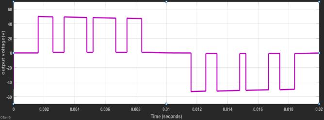
Thefigure7showstheoutputvoltagewaveformobtained from the MATLAB/Simulink simulation of the multilevel inverter. The horizontal axis represents time in seconds, whiletheverticalaxisrepresentstheoutputvoltageinvolts. Thewaveformexhibitsasteppedvoltagepattern,whichis characteristic of multilevel inverter operation. During the positivehalfcycle,theoutputvoltageswitchesbetweenzero and a positive voltage level (approximately +50 V), while duringthenegativehalfcycleitswitchesbetweenzeroanda negativevoltagelevel(approximately−50V).Thesevoltage levelsareproducedbycontrollingtheswitchingstatesofthe power semiconductor devices in the inverter using pulse widthmodulation(PWM)signals.
Fig. 8 illustrates the MATLAB/Simulink model of a threelevelFlyingCapacitorMultilevelInverter(FCMLI)alongwith its PWM control circuit and load configuration. In the left sectionofthemodel,thecontrolcircuitgeneratesswitching signalsusingthePulseWidthModulation(PWM)technique. Asinewaveblockactsasthereferencesignalrepresenting thedesiredACoutputwaveform,whilerepeatingsequence blocks generate high-frequency triangular carrier signals. Thesesignalsarecomparedusingrelationaloperatorblocks, whichproducePWMswitchingpulses.Thegeneratedgate signalsarethentransmittedthroughGotoandfromblocksto controltheswitchingdevicesintheinvertercircuit.
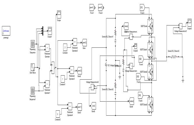
Therightsectionofthemodelrepresentsthepowercircuit of the flying capacitor multilevel inverter. A DC voltage sourceprovidestheinputsupply,andtheinverterconsistsof fourIGBTswitcheswithanti-paralleldiodes(S1,S2,S3,and S4).Aflyingcapacitorisconnectedbetweentheswitching nodes,whichstoresenergyandhelpsgenerateintermediate voltage levels during switching operation. By properly controllingtheswitchingstatesoftheIGBTsusingthePWM signals, the inverter produces three output voltage levels (+Vdc/2,0,and−Vdc/2).Theoutputisconnectedtoaseries
International
Volume: 13 Issue: 04 | Apr 2026 www.irjet.net p-ISSN: 2395-0072
Rload,andvoltagemeasurementblocksandscopedisplays are used to observe the inverter output waveform. This configuration demonstrates how the flying capacitor multilevel inverter converts DC power into a stepped AC voltage with improved waveform quality and reduced harmonicdistortion.
Thefigure9illustratesthereferenceandcarriersignalsused inthePulseWidthModulation(PWM)controltechniquefor the multilevel inverter. In the waveform, the red curve represents the sinusoidal reference signal, which corresponds to the desired AC output waveform of the inverter. The green and purple triangular waveforms represent the high-frequency carrier signals used for comparison in the PWM process. These carrier signals operateatamuchhigherfrequencythanthereferencesine waveandareusedtogeneratetheswitchingpulsesrequired forcontrollingtheinverterswitches.
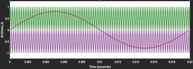
Fig -9:CarrierandreferencesignalsusedforPWM switchingintheinvertercontrolcircuit.
During operation,the reference sine wave iscontinuously compared with the carrier triangular signals using comparator or relational operator blocks. When the reference signal is greater than the carrier signal, the correspondingswitchisturnedON,andwhenitislower,the switchisturnedOFF.Thiscomparisonprocessgeneratesthe PWMgatesignalsrequiredfortheswitchingdevicesinthe inverter circuit. The use of multiple carrier signals helps producemultiplevoltagelevelsintheoutputwaveform.Asa result,the invertercan generate a steppedACoutputthat closely approximates a sinusoidal waveform, thereby reducingharmonicdistortionandimprovingpowerquality inthemultilevelinvertersystem.
The figure 10 shows the PWM gate pulse waveform generated for controlling the inverter switches in the multilevel invertersystem. The horizontal axis represents timeinseconds,whiletheverticalaxisrepresentsthelogic leveloftheswitchingsignal.Thewaveformconsistsofhighfrequency pulses that alternate between different logic levels, indicating the ON and OFF states of the inverter switchingdevices.Inthefirsthalfofthecycle,theswitching pulsesvarybetweenhigherlogiclevels,whileinthesecond halftheyswitchbetweenlowerlevels,correspondingtothe positive and negative halves of the reference sinusoidal signalusedinthePWMcontrolscheme.
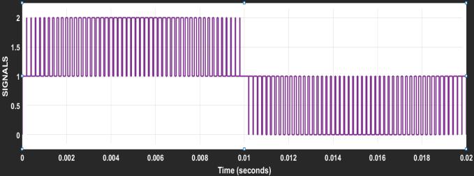
Thesepulsesaregeneratedbycomparingthereferencesine wave with carrier triangular signals in the PWM control circuit.Whenthereferencesignalisgreaterthanthecarrier signal,thecorrespondingswitchreceivesanONpulse,and when it is lower, the switch turns OFF. The varying pulse widthsindicatethepulsewidthmodulationprocess,which controls the inverter switching pattern. These gate pulses are applied to the IGBT switches in the inverter circuit, enabling the generation of stepped output voltage levels. This switching technique helps the multilevel inverter produceanoutputwaveformthatapproximatesasinusoidal waveform, thereby reducing harmonic distortion and improvingtheoverallpowerquality.
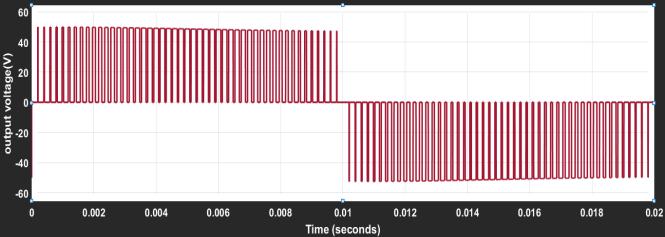
Thefigure11showstheoutputvoltagewaveformobtained from the MATLAB/Simulink simulation of the multilevel inverter system. The horizontal axis represents time in seconds,whiletheverticalaxisrepresentstheoutputvoltage in volts. The waveform consists of high-frequency pulses whoseamplitudealternatesbetweenpositiveandnegative voltagelevels,indicatingtheinverter’sswitchingoperation. During the positive halfcycle,the outputvoltage switches between 0 V and approximately +50 V, while during the negative half cycle it switches between 0 V and approximately −50 V. These pulses are produced by the PWM (Pulse Width Modulation) control technique, where switching devices such as IGBTs are turned ON and OFF accordingtothegeneratedgatesignals.Therapidswitching createsapulsedwaveformthatapproximatesasinusoidal AC output when filtered or applied to the load. This switchingpatterndemonstrateshowtheinverterconverts DCinputvoltageintoanACoutputvoltagewithcontrolled amplitude and reduced harmonic distortion, which is
International Research Journal of Engineering and Technology (IRJET) e-ISSN: 2395-0056
Volume: 13 Issue: 04 | Apr 2026 www.irjet.net p-ISSN: 2395-0072
essentialforimprovingpowerqualityinmultilevelinverter systems.
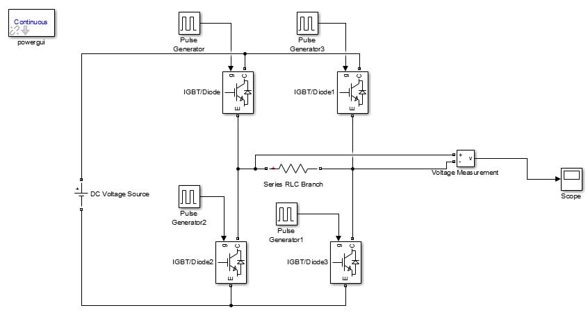
Thefigure12illustratesAcascadedH-bridge(CHB)3-level inverterisatypeofmultilevelinverterthatproducesthree distinct output voltage levels, namely +Vdc, 0, and −Vdc, usingasingleH-bridgecellinasingle-phaseconfiguration. The H-bridge consists of four power electronic switches, typicallyIGBTswithanti-paralleldiodes,connectedtoaDC voltage source.Bycontrollingthe switchingsequence,the inverter generates different voltage levels: when the diagonalswitches(S1andS4)areturnedON,theoutputis +Vdc;whentheoppositediagonalswitches(S2andS3)are ON,theoutputbecomes−Vdc;andwheneithertheupperor lowerpairofswitchesisactivated,theoutputiszero.This steppedoutputwaveformisclosertoasinusoidalwaveform comparedtoaconventionaltwo-levelinverter,resultingin reducedharmonicdistortionandimprovedpowerquality. TheCHBtopologyismodular,efficient,andwidelyusedin applications such as renewable energy systems, electric vehicles, and motor drives, although it requires proper switchingcontroland,forhigherlevels,multipleisolatedDC sources.
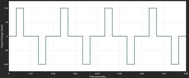
Thefigure13showstheoutputvoltagewaveformrepresents theoutputvoltageofathree-levelcascadedH-bridge(CHB) inverter, where the voltage alternatesamong+100 V,0 V, and−100Vinaperiodicsequence.Thissteppedwaveformis
produced by appropriate switching of the IGBTsin the Hbridge, such that the positive level is obtained when one diagonalpairofswitchesconducts,thenegativelevelwhen theoppositepairconducts,andthezerolevelwheneither the upper or lower switches are turned on together. The presence of the zero state between positive and negative levels results in a waveform that is closer to a sinusoidal shape compared to a conventional two-level inverter, therebyreducingharmonicdistortionandimprovingoutput quality.Thewaveformissymmetricalinbothpositiveand negative halves, indicating balanced operation and a constantDCinput,anditsperiodicnaturecorrespondstoa typicalfundamentalfrequencyusedinpowerapplications.
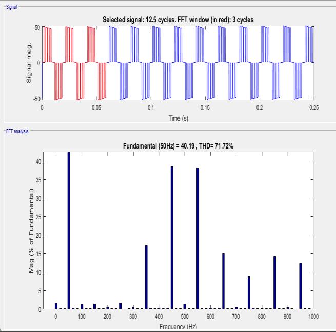
The figure 14 illustrates both the time-domain output waveformofaninverteranditscorrespondingfrequencydomain analysis using Fast Fourier Transform (FFT), providing a comprehensive understanding of the signal characteristics. In the upper portion of the figure, the inverter output voltage is shown as a stepped alternating waveform, which is typical of multilevel inverter configurations.Thewaveformalternatesbetweenpositive and negative voltage levels with intermediate transitions, indicatingcontrolledswitchingofpowerelectronicdevices such as IGBTs. A specific portion of the waveform, highlighted in red, is selected for FFT analysis, while the remainingpartisshowninbluetorepresentthecontinuity of the signal over multiple cycles. This selection ensures accurate harmonic analysis by focusing on a steady-state segmentofthewaveform.
Inbarrepresentation
In the lower portion, the FFT spectrum presents the frequency components of the selected signal, where the horizontalaxisrepresentsfrequencyinhertzandthevertical axisindicatesthemagnitudeofeachharmoniccomponentas
International Research Journal of Engineering and Technology (IRJET) e-ISSN: 2395-0056
Volume: 13 Issue: 04 | Apr 2026 www.irjet.net p-ISSN: 2395-0072
apercentageofthefundamental.Thefundamentalfrequency isobservedatapproximately50Hz,whichisstandardfor manypowersystems,whilemultipleharmoniccomponents appearathigherfrequencies.TheTotalHarmonicDistortion (THD)iscalculatedtobearound71.2%,whichisrelatively highandindicatesthatthewaveformdeviatessignificantly fromanidealsinusoidalshape.SuchahighTHDimpliesthe presence of strong harmonic components that can lead to increasedpowerlosses,andreducedoverallefficiencyofthe system.
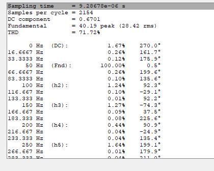
Thefigure15presentsthenumericalFFTanalysisresultsof the diode-clampedmultilevel inverteroutputvoltage.The samplingtimeis9.28678×10⁻⁶seconds,with2154samples per cycle, ensuring accurate harmonic evaluation. The fundamentalcomponentat50Hzhasapeakvalueof40.19V and an RMS value of 28.42 V. The table also lists the magnitude and phase angles of various harmonic components such as second, third, fourth, and fifth harmonics. These harmonics arise due to the switching characteristicsofthediode-clampedinverter.FFTanalysisis used to evaluate the harmonic performance and power qualityoftheDCMLIsystem,andtheTHDvalueprovidesan indication of the distortion present in the inverter output waveform.
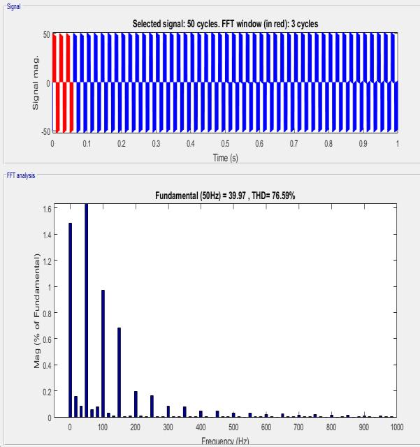
The figure 16 shows the FFT (Fast Fourier Transform) analysis of the output voltage waveform of the Flying Capacitor Multilevel Inverter (FCMLI) obtained from the MATLAB/Simulinksimulation.Theupperplotpresentsthe time-domainwaveformoftheinverteroutputvoltage,where aportionofthesignalisselectedforharmonicanalysis.The red-highlightedsectionindicatestheFFTanalysiswindow,
which contains three cycles of the waveform used to computetheharmonicspectrum.Thelowergraphillustrates the frequency spectrum of the output voltage, where the magnitudeofeachharmoniccomponentisplottedagainst frequency. The analysis shows that the fundamental frequencyoftheinverteroutputis50Hzwithamagnitude of39.97,andthecalculatedTotalHarmonicDistortion(THD) is76.59%,indicatingthepresenceofsignificantharmonic componentsinthewaveform.
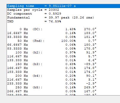
The Fig 17 represents numerical FFT results provide additionaldetailsabouttheharmoniccontentoftheflying capacitormultilevelinverteroutputvoltage.Thesampling time is 9.85111 × 10⁻⁷ seconds, with 20302 samples per cycle, ensuring high accuracy in frequency analysis. The fundamentalcomponentat50Hzhasapeakvalueof39.97V andanRMSvalueof28.26V.
International Research Journal of Engineering and Technology (IRJET) e-ISSN: 2395-0056
Volume: 13 Issue: 04 | Apr 2026 www.irjet.net p-ISSN: 2395-0072
The table also lists the magnitude and phase angles of several harmonic components such as 100 Hz (second harmonic), 150 Hz (third harmonic), 200 Hz (fourth harmonic), and 250 Hz (fifth harmonic). These harmonics are generated due to the switching action of the inverter devicesandthe PWM control technique used in the flying capacitor topology. The FFT analysis is therefore used to evaluatetheharmonicperformanceandpowerqualityofthe flying capacitor multilevel inverter, and the THD value of 76.59% indicates the level of distortion present in the inverteroutputwaveform.
The figure 18 illustrate the FFT (Fast Fourier Transform) analysisoftheoutputvoltagewaveformoftheCascadedHBridge Multilevel Inverter (CHBMLI) obtained from the MATLAB/Simulink simulation. The upper plot shows the time-domainoutputvoltagewaveform,whereaportionof the signal is selected for harmonic analysis. The redhighlighted section represents the FFT analysis window, which contains three cycles of the waveform used to determinetheharmonicspectrum.Thesteppedwaveform clearly indicates the multilevel nature of the cascaded Hbridge inverter, where multiple H-bridge cellscombine to produceseveralvoltagelevelsthatapproximateasinusoidal waveform.
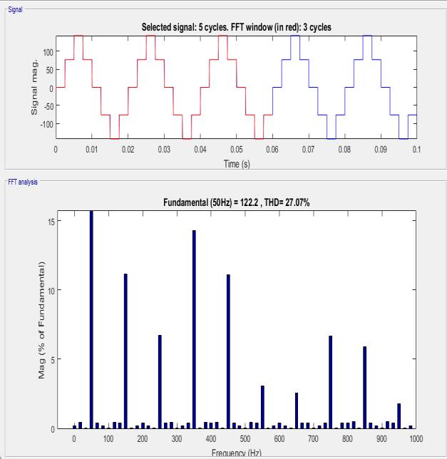
Fig -18:THDofCascadedHBridgeMultilevelInverterin Barrepresentation.
The lower graph presents the frequency spectrum of the output voltage, where the magnitude of each harmonic componentisplottedwithrespecttofrequency.Theanalysis shows that the fundamental frequency is 50 Hz with a magnitude of 122.2, and the calculated Total Harmonic Distortion (THD) is 27.07%, indicating a significant reductioninharmonicdistortioncomparedtootherinverter topologies
The figure 19 illustrates numerical FFT results provide detailed information about the harmonic components
presentinthecascadedH-bridgemultilevelinverteroutput voltage.Thesamplingtimeis9.56023×10⁻⁵seconds,with 209samplespercycleusedintheanalysis.Thefundamental componentat50Hzhasapeakvalueof122.2VandanRMS valueof86.44V.Theharmonictableliststhemagnitudeand phase angles of several harmonics such as 150 Hz (third harmonic), 200 Hz (fourth harmonic), and 250 Hz (fifth harmonic). These harmonics arise due to the switching operation of the MOSFET devices in each H-bridge cell. Compared with other multilevel inverter topologies, the cascadedH-bridgeinverterproducesalowerTHDvalueof 27.07%, demonstrating improved waveform quality and better power quality performance due to its ability to generatemultiplevoltagelevelsattheoutput.
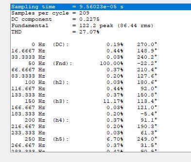
Fig -19:THDofCascadedHBridgeMultilevelInverterIn listrepresentation.
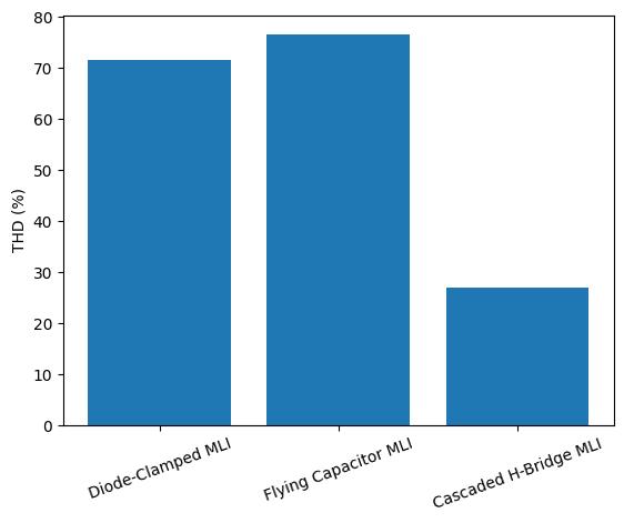
The figure shows a bar graph representing the Total Harmonic Distortion (THD) comparison of different multilevel inverter topologies obtained from MATLAB/Simulink simulation results. The horizontal axis represents the three inverter types: Diode-Clamped Multilevel Inverter (DCMLI), Flying Capacitor Multilevel Inverter(FCMLI),andCascadedH-BridgeMultilevelInverter (CHBMLI), while the vertical axis represents the THD percentageoftheoutputvoltagewaveform.Fromthegraph, theflyingcapacitormultilevelinverterexhibitsthehighest THDof76.59%,followedbythediode-clampedmultilevel inverter with 71.72% THD, indicating higher harmonic distortion in their output waveforms. In contrast, the cascadedH-bridgemultilevelinvertershowsthelowestTHD valueof27.07%,whichmeansitproducesawaveformthat is closer to a sinusoidal signal. This comparison demonstratesthatthecascadedH-bridgeinverterprovides betterharmonicperformanceandimprovedpowerquality comparedtothediode-clampedandflyingcapacitorinverter topologies.
International Research Journal of Engineering and Technology (IRJET) e-ISSN: 2395-0056
Volume: 13 Issue: 04 | Apr 2026 www.irjet.net p-ISSN: 2395-0072
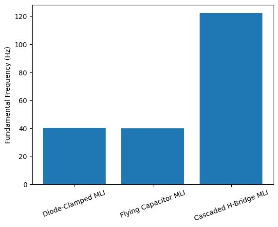
The figure 20 shows a bar graph representing the fundamental frequencycomparison ofdifferent multilevel inverter topologies obtained from simulation results. The horizontal axis indicates the three inverter types: DiodeClamped Multilevel Inverter (DCMLI), Flying Capacitor Multilevel Inverter (FCMLI), and Cascaded H-Bridge Multilevel Inverter (CHBMLI), while the vertical axis representsthefundamentalfrequencyinHertz(Hz).From the graph, both the diode-clamped and flying capacitor multilevel inverters operate at approximately 40 Hz, showingsimilarfundamentalfrequencycharacteristics.In contrast,thecascadedH-bridgemultilevelinverterproduces ahigherfundamentalfrequencyofabout122.2Hz.
Inthisproject,theperformanceofthreemultilevelinverter topologies Diode-Clamped Multilevel Inverter (DCMLI), FlyingCapacitorMultilevelInverter(FCMLI),andCascaded H-BridgeMultilevelInverter(CHBMLI) wasanalyzedand comparedusingMATLAB/Simulink simulation,with Total Harmonic Distortion (THD) as the main comparison parameter.ThesimulationresultsandFFTanalysisshowed that multilevel inverters produce stepped output voltage waveformsthatcloselyapproximateasinusoidalwaveform, thereby improving power quality. Among the three topologies, the Cascaded H-Bridge Multilevel Inverter exhibited better harmonic performance with lower THD compared to the diode-clamped and flying capacitor inverters. Multilevel inverters provide several advantages such as reduced harmonic distortion, improved output voltagequality,lowerswitchingstressonpowerdevices,and reducedelectromagneticinterference.Theyalsoallowhighvoltageoperationusinglower-ratedsemiconductordevices, which improves system efficiency and reliability. Due to these advantages, multilevel inverters are widely used in applications such as renewable energy systems, motor drives, electric vehicles, and high-power industrial power conversionsystems.
[1] J. Rodriguez, J. S. Lai, and F. Z. Peng, “Multilevel Inverters: A Survey of Topologies, Controls, and Applications,” IEEE Transactions on Industrial Electronics,vol.49,no.4,pp.724–738,Aug.2002.
[2] M.H.Rashid,PowerElectronics:Circuits,Devices,and Applications,3rded.,PearsonEducation,2004.
[3] S. Kouro, M. Malinowski, K. Gopakumar, J. Pou, L. G. Franquelo,B.Wu,J.Rodriguez,M.Perez,andJ.I.Leon, “Recent Advances and Industrial Applications of MultilevelConverters,”IEEETransactionsonIndustrial Electronics,vol.57,no.8,pp.2553–2580,Aug.2010.
[4] L.M.Tolbert,F.Z.Peng,andT.G.Habetler,“Multilevel ConvertersforLargeElectricDrives,”IEEETransactions onIndustryApplications,vol.35,no.1,pp.36–44,Jan.–Feb.1999.
[5] J.Rodriguez,S.Bernet,B.Wu,J.O.Pontt,andS.Kouro, “Multilevel Voltage-Source-Converter Topologies for IndustrialMedium-VoltageDrives,”IEEETransactions onIndustrialElectronics,vol.54,no.6,pp.2930–2945, Dec.2007.
[6] B. Wu, High-Power Converters and AC Drives, IEEE Press/Wiley,2006.
Thiscomparisonhighlightsthedifferenceinoutput frequencycharacteristicsamongthethreeinverter topologiesandindicatesthatthecascadedH-bridge inverterprovidesahigherfundamentalfrequencyinthe simulatedsystem,whichcontributestoimproved waveformformationwhencombinedwithitslower harmonicdistortion.
[7] M. Malinowski, K. Gopakumar, J. Rodriguez, and M. A. Perez,“ASurveyonCascadedMultilevelInverters,”IEEE TransactionsonIndustrialElectronics,vol.57,no.7,pp. 2197–2206,July2010.
[8] N. Mohan, T. M. Undeland, and W. P. Robbins, Power Electronics: Converters, Applications, and Design, 3rd ed.,Wiley,2003.
[9] F.Z.Peng,“AGeneralizedMultilevelInverterTopology with Self Voltage Balancing,” IEEE Transactions on
International Research Journal of Engineering and Technology (IRJET) e-ISSN: 2395-0056
Volume: 13 Issue: 04 | Apr 2026 www.irjet.net p-ISSN: 2395-0072
IndustryApplications,vol.37,no.2,pp.611–618,Mar.–Apr.2001.
[10] J.S.LaiandF.Z.Peng,“MultilevelConverters ANew Breed of Power Converters,” IEEE Transactions on IndustryApplications,vol.32,no.3,pp.509–517,May–June1996.
[11] A. Nabae, I. Takahashi, and H. Akagi, “A New NeutralPoint-Clamped PWM Inverter,” IEEE Transactions on Industry Applications, vol. IA-17, no. 5, pp. 518–523, Sept.–Oct.1981.
[12] P. Hammond, “A New Approach to Enhance Power Quality for Medium Voltage AC Drives,” IEEE TransactionsonIndustryApplications,vol.33,no.1,pp. 202–208,Jan.–Feb.1997.
[13] L. G. Franquelo, J. Rodriguez, J. I. Leon, S. Kouro, R. Portillo, and M. A. Prats, “The Age of Multilevel Converters Arrives,” IEEE Industrial Electronics Magazine,vol.2,no.2,pp.28–39,June2008.
[14] S. Kouro, J. Rodriguez, B. Wu, S. Bernet, and M. Perez, “Powering the Future of Industry: High-Power Adjustable Speed Drive Topologies,” IEEE Industry Applications Magazine, vol. 18, no. 4, pp. 26–39, July–Aug.2012.