5 minute read
International Journal for Research in Applied Science & Engineering Technology (IJRASET)

from Development of a Bidirectional DC-DC Converter with Dual-Battery Energy Storage for hybrid Electric
by IJRASET

ISSN: 2321-9653; IC Value: 45.98; SJ Impact Factor: 7.538
Volume 11 Issue III Mar 2023- Available at www.ijraset.com
Advertisement
C.
The voltage gains of the proposed BDC can be derived by applying the principle of inductor volt-second balance to the different modes. To enhance simplicity and practicality, the equivalent series resistances (ESRs) of the inductors L1 and L2 have been substituted into the state equations as nonideal cases, and the parameters RL1=RL2=RL=50mΩ are also given
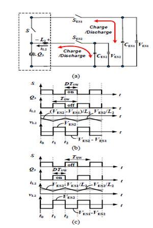
D. Low-Voltage Dual-Source-Powering Mode where VRL is the voltage difference across the ESR of inductance, k is the ratio of Vs1 =VES1 to Vs2 =VES2, and Du is the duty cycle of Q3 and Q4 and is >50%.
The relationship among the voltage gains of the three dc sources under steady-state operation are given by (17) and (18).
Using (17) and (18), the ideal static voltage gains of VH/Vs1 and VH/Vs2 can be expressed as (19) and (20).
ISSN: 2321-9653; IC Value: 45.98; SJ Impact Factor: 7.538
Volume 11 Issue III Mar 2023- Available at www.ijraset.com
Accordingly, the relation between dc-bus voltage VH and the dual-source voltages (VES1, VES2) is given by (21).
E. High-Voltage DC-Bus Energy-Regenerating Mode
Under steady-state operation, the relationship among the voltage gains of the three dc sources are given by where Dd is the duty cycle of Q1 and Q2 and is <50%. From (22) and (23), the ideal static voltage gains of Vs1/VH and Vs2/VH are given as (24) and (25)
Accordingly, the relation between the dual-source voltages (VES1, VES2) and the dc-bus voltage VH is given by (26).
Although these voltage gains are reduced by the ESR of the inductors under the nonideal situation, the parasitic effect is relatively small and thus the reduced voltage gain can be easily compensated for by increasing the duty control. In order to test the dynamic performance of the system, a load profile is chosen according to normalized ECE-15 driving cycle [25]; the analyzed section of this driving cycle is demonstrated in Fig,. This period is chosen to examine the system under maximum power demand and in the presence of regenerative braking energy. The load profile is created by utilizing dc load bank and dc generator which are shown in Fig.
Moreover, simulations are carried out via developed PSIM switching model including switch turn-ON resistances and output capacitor equivalent serial resistance; in the simulation, battery and UC are modeled as in. Note that in both cases battery and UC initial voltages are set to 38 V and 33.6 V (70% state-of-charge), respectively. Figs. 19-21 compare the experimental and simulation results. In Fig, the output voltage and output current are shown. Here, it is clear that the output voltage is successfully regulated at 48 V in both cases. Moreover, the fact that output current in the experiment and simulation match well indicates that the output power is adjusted as intended by load bank and generator Fig. shows the battery and UC average current. From Fig. 20, it can be noticed that the battery current variations in the experiment and in the simulation appear similar. In both cases maximum battery current is limited to 20 A due to the control strategy; at this instant, UC current is increased for compensating the load demand. Additionally, UC current becomes negative when it stores regenerative braking energy.Fig. highlights the input source voltages. This figure indicates that battery voltage as well as UC voltage in the experiment and in the simulation change in a similar way. Because of its equivalent serial resistance, battery voltage decreases substantially when it gives power. In addition to that, UC voltage decreases when it compensates load demand and increases when it is charged. The voltage and current of Q0 body diode are illustrated in one can see that when T0 is OFF, the diode starts to conduct as can be understood from its positive current. Conversely, when S0 is ON, the diode becomes OFF thus its current goes to zero. Illustrate the measured steady state waveforms when the converter operates in the charging mode. In this test, by controlling Q0 switch, the output voltage is again kept at 48 V while UC is charged under 400W constant power. Based on these figures, it can be asserted that the experimental results match the theoretical waveforms given in Fig. 4. Fig. 15 shows the experimental results of Q0 terminal voltages at steady state. In Fig.15, the duty cycle of Q0 is about 0.8 as expected according to (10) which explains the relationship between the duty cycle of Q0, UC voltage (~40V), and the output voltage. Figs. 15-16 illustrate the measured steady state waveforms when the converter operates in the charging mode. In this test, by controlling Q0 switch, the output voltage is again kept at 48 V while UC is charged under 400W constant power.
ISSN: 2321-9653; IC Value: 45.98; SJ Impact Factor: 7.538
Volume 11 Issue III Mar 2023- Available at www.ijraset.com
Based on these figures, it can be asserted that the experimental results match the theoretical waveforms given in Fig. 5.3. Fig. shows the experimental results of Q0 terminal voltages at steady state. In Fig., the duty cycle of Q0 is about 0.8 as expected according to (10) which explains the relationship between the duty cycle of Q0, UC voltage (~40V), negative since UC is charged. Moreover, when Q0 is turned ON, the voltage of the inductor becomes negative thus its current increases (negatively); conversely, turning it OFF makes the voltage of the inductor equal to UC voltage and decreases its current (negatively). Fig illustrates the proposed converter efficiency curves for the discharging and charging modes which are obtained by power analyzer. In the discharging mode, the power of one source is set to 200 W while other source is utilized to compensate the load demand. Besides, in the charging mode,dc bus is regulated when adjusting the charging power of the and the output voltage In Fig., the voltage and current variations of L2 are demonstrated. It can be noticed that the inductor current
F. Low-Voltage Dual-Source Buck/Boost Mode
The relation between the two low-side voltages is given by (27).
In (27), Ds is the duty cycle of S for the energy transferred from the main energy storage to the auxiliary energy storage, whereas D is the duty cycle of Q3 for the energy transferred from the auxiliary energy storage to the main energy storage. The relationship between the two low-side voltages without the effect of the ESR of inductors can be expressed as (28).
In (27), Ds is the duty cycle of S for the energy transferred from the main energy storage to the auxiliary energy storage, whereas D is the duty cycle of Q3 for the energy transferred from the auxiliary energy storage to the main energy storage. The relationship between the two low-side voltages without the effect of the ESR of inductors can be expressed as (28).
G. Charge-Pump Voltage
The voltage across the CB under different modes can be derived as follows.
1) Low-Voltage Dual-Source-Powering Mode
2) High-Voltage DC-Bus Energy-Regenerating Mode
H. Voltage Stresses on Switches
To simplify the voltage stress analyses of the converter, the voltage ripples on the capacitors were ignored. As shown in Figs. 4, 6, 8, and 9, the maximum voltage stresses of the main power MOSFETs Q1~Q4 can be obtained directly as (33)-(36)
ISSN: 2321-9653; IC Value: 45.98; SJ Impact Factor: 7.538
Volume 11 Issue III Mar 2023- Available at www.ijraset.com
I. Characteristic of Uniform Average Current Sharing
Through charge balance principles and the state-space averaging technique, the averaged state equations can be obtained directly as where IH=VCH/RH.
From (37)-(39), the following equation can be obtained:
From, the uniform average current sharing can be determined, independent of the values of the capacitors.
IV.SIMULATIONRESULTS
A. Existing Results
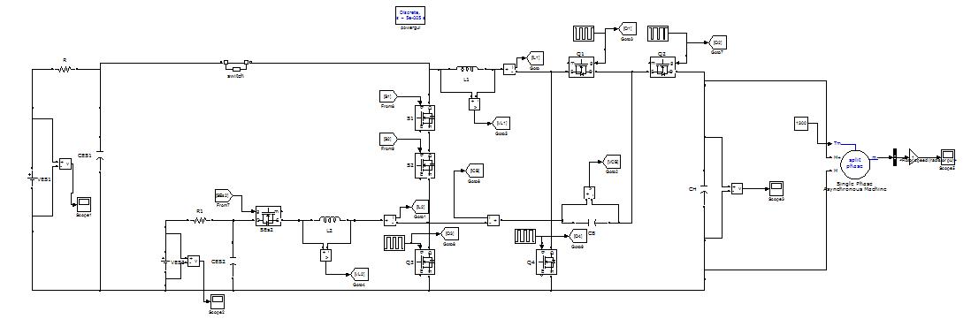
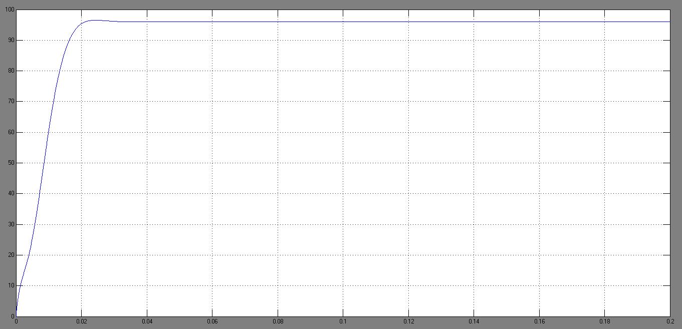
Fig 9. indicates the MATLAB/SIMULINK circuit diagram of proposed bidirectional DC/DC converter, Fig 10. shows the Lowvoltage dual sources (a) VES1 (b) VES2, Fig 11. shows the DC-bus voltage, Fig 12. shows the motor speed.