No part of this publication may be reproduced in whole or in part in any medium without the express permission of the publisher.
For editorial enquiries email contribute@fpgahorizons.com
For advertising enquiries email advertise@fpgahorizons.com
Welcome to issue 4 of the FPGA Horizons Journal
The latest issue continues to explore what’s happening now in FPGA design and development, and the trends and technologies that continue to shape its future. And once again there’s a lot to talk about.
Are FPGAs secure in the cloud, for example? Professor Dirk Koch, who leads the fascinating Novel Computing Technologies Group at Heidelberg University, decided to find out and the results of his research make for an interesting, if slightly worrying, read.
How can FPGAs break the constraints of DDR-driven architectures that dictate device and board design, and limit system performance? Mike Rather from AMD introduces an innovative approach that places high-bandwidth LPDDR5 directly alongside the FPGA die and fundamentally changes the rules of FPGA system design. (That’s not hyperbole, by the way. I’m genuinely intrigued by it.)
And how do you handle the tens to hundreds of megabytes of timing reports, congestion maps, Design Rule Check (DRC) logs, etc, generated by modern EDA workflows? Kevin Hubbard from Black Mesa Labs shows how Ash, a new open-source AI assistant, comes to the rescue.
Those are just three of the stories in this issue. You can also find out how to migrate from a legacy FPGA, why understanding the role of post-layout signal integrity really is crucial, and a lot more.
You may also notice there’s no Industry roundup this issue. That’s because one story has been rippling through the technology media over the last three months that’s bigger than any of the other announcements, news and updates. (Even the inspiring story about how a group of students at Cornell University created an FPGA implementation of the original Bletchley Park Bombe machine to break Enigma codes. Visit Hackaday.com and search for “breaking Enigma” to find out more.) Even that has been eclipsed by the chip shortage.
So in an editorial article for this issue, we find out what’s causing the chip shortage, what the impact on the FPGA supply chain is, and what the implications are, both now and in the future for FPGA design.
We hope you enjoy the latest journey of discovery.
Matt Hilbert Editor
In Issue 4
Matt HIlbert (editor) looks at Why the chip shortage means FPGA designs need a Plan B
Prof. Dirk Koch (Heidelberg University) reveals How to render cloud FPGAs useless (and why it’s surprisingly hard to kill one)
Mike Rather (AMD) explains why we need to be Rethinking how we build high-performance FPGA/ adaptive SoCs
Rachael Peterson (Concurrent Technologies PLC) takes us through Migrating from a legacy FPGA to a modern scalable platform
Dan Binnun (E3 Designers) talks about Validating your FPGA design: the role of post-layout signal integrity
Kevin Hubbard (Black Mesa Labs) introduces Ash, the open-source AI assistant for processing
Marius Elvegård (Inventas) discusses Hidden verification errors and how UVVM finds them
Dr. Pierre Maillard & Dr. Abhijitt Dhavlle (AMD) explore Validating single event resilience
Oliver Bründler (OpenLogic) proposes Designing
Disclaimer
The content published in the FPGA Horizons Journal is contributed by independent authors and researchers. While we strive to ensure accuracy and maintain a standard of quality, the views and opinions expressed in individual articles are those of the respective contributors and do not necessarily reflect the views of the FPGA Horizons Journal editorial team or its affiliates.
We are committed to using neutral and inclusive language wherever possible. However, given the diversity of voices and topics, variations in tone and expression may occur. The FPGA Horizons Journal does not accept responsibility for any errors, omissions, or differing viewpoints presented in the submitted content.
Readers are encouraged to critically engage with the material and consult additional sources where appropriate.
W hy the chip shortage means FPGA designs need
a
PLAN
BMatt Hilbert, Editor
There’s a technology landgrab going on. The race for bigger, better, faster AI needs more and more compute power. McKinsey predicts that spending on datacenters to feed AI will reach $6.7 trillion worldwide by 2030 just to keep up. That’s more than the GDP of Germany, the world’s third-largest economy. Oh, and annual global datacenter power demand will also rise from 460 TWh in 2024 to over 1,000 TWh in 2030 according to the International Energy Agency (IEA). That’s enough to power Japan … er, all of Japan.
The thing is, a large slice of the spending is going into the hardware that makes AI possible: advanced-node semiconductors, High Bandwidth Memory (HBM), custom AI accelerators, and advanced packaging. The same kind of hardware used in FPGAs as well as mobile phones, laptops, GPUs, and automotive electronics.
And we’re already seeing the ripples it’s causing. In 2026, datacenters are expected to buy up 70 percent of memory chips produced, up from around 30% in 2022. Companies like Micron, SK Hynix and Samsung have shifted their production capacity away from the consumer-friendly DRAM to the more profitable HBM to meet the demand. As a result, Gartner has predicted PC prices will rise by 17% and smartphone prices by 13%. There’s even a new word for it: the ‘RAMpocalypse’.
It’s happening for FPGAs as well. With foundries prioritizing the manufacture of advanced nodes, high-end FPGA devices have dropped down the queue. Meanwhile, legacy and mainstream FPGAs are marooned on mature wafer nodes where capacity expansion has stalled for years, and foundries are reallocating their remaining capacity to more profitable power-management ICs for AI servers. The result is that across almost all device classes, lead times have increased from around eight weeks to 52 weeks and longer.
And in an ironic plot twist worthy of a bad B-movie, the shortage of FPGAs caused by the increasing demand for those advancednode semiconductors has limited the supply of FPGAs needed for the equipment to test … semiconductors. How’s that for schadenfreude at work?
Welcome to change … again
None of this is new. We saw a similar situation when the COVID-19 pandemic started in early 2020. Labor shortages, lockdowns and foundry shutdowns broke the supply chain for semiconductors and FPGAs, and costs and lead times increased. Shipping delays and shortages in raw materials caused problems throughout the whole manufacturing process and Bills of Materials (BoMs) became a guessing game. The surge in cloud usage from late 2020 onwards then saw the datacenter and telecommunications sectors buy up available FPGA supplies, leaving other sectors to pick up what little was left.
In many ways, however, it is new. This is not a temporary glitch, it’s a structural shift to a different kind of computing that needs a whole new infrastructure to be built, equipped and maintained over what looks like the long term.
PwC and McKinsey have been analyzing what’s been happening in the semiconductor market and they concur in their opinions. PwC’s 2026 Semiconductor and beyond report and McKinsey’s January 2026 Hiding in plain sight analysis both cite computing and data storage as the fastest growing sector, with AI datacenters and servers a major factor in that growth. PwC expects the revenue share of AI accelerators in datacenter chips to grow rapidly and reach around 50 percent of the total. McKinsey goes further and estimates 62 percent of total growth will stem from leading-edge chips, primarily for AI.
In terms of numbers, PwC forecasts the global semiconductor market will grow from $627 billion in 2024 to $1,030 billion in 2030. McKinsey is more bullish and predicts it will increase from $775 billion to $1,600 billion. Either way, it shows the growth is here, it’s now – and its effect on the supply chain will continue for the coming years.
Both, however, are behind the curve. There is now a brutal supply and demand problem with datacenter hyperscalers fighting over a finite supply of semiconductors. In its Spring 2026 forecast, the World Semiconductor Trade Statistics (WSTS) organization predicted the global semiconductor market would grow beyond $1,500 billion in 2026, and reach approximately $1,900 billion in 2027.
Rather than demonstrating another increase in unit demand, however, a large part of that comes from a surge in prices, with chip makers seeing meteoric rises in revenue. The revenue of Micron and SK Hynix has doubled year-on-year, while Samsung has seen a jump of ~130%.
Quite simply, the market isn’t shipping more semiconductors, it’s charging more for them, showing how tight the supply is – and how strong the demand is.
It’s
time for that B
PLAN
Not normal has suddenly become the new normal. Unlike the pandemic, the current global chip and FPGA shortage hasn’t faded, it’s evolved. AI is taking over advanced node capacity, there are queues around the block for packaging and test lines, and even PCB costs are rising. The result? The FPGA you want may not be the FPGA you can get, and even entire device families may no longer be available.
The old assumption that you could choose one device, optimize around it and order it when you need it may no longer work. The new normal brings uncertainty into the equation. For some, flexibility may move from an option to an ongoing design challenge. That calls for rethinking how to approach FPGA design so that you have a Plan B. An option to move to if your first choice isn’t available.
Think about constraint-driven design
Many FPGA engineers have a particular liking for one kind of FPGA, or family of FPGAs. It may be familiarity, it may be that it’s easier to work with, it may simply be We’ve always done it this way. It’s time for a change of tack. With uncertain supply chains, a constraint-driven design approach offers more options. Keep that favored FPGA in mind so you have a goal to aim for but be prepared to move on if you have to.
Constraint-driven design thinks in terms of envelopes rather than specific devices. It defines the timing, resource, I/O, power and thermal, and latency budgets designs must operate within. Any FPGA that meets those envelopes then becomes a viable candidate. To make that possible, interfaces must be kept modular and technology neutral, and the power, clocking and PCB topology designed to accommodate the range of devices in the envelope. When the architecture is built this way, switching devices doesn’t require structural change. Only the device-specific wrappers need to be adapted.
It also opens up fallback options across vendors, families, grades and packages, turning a single device dependency into a set of practical alternatives. In practice, it can transform a 52 week lead time into a 12 week pivot to a different device. No promises on that one, but you get the picture.
2Design for substitution
The next step is to treat FPGA substitution as a normal part of the engineering process rather than an emergency workaround, by designing the system so that changing devices is routine, predictable and contained. The goal is not universal portability, but controlled substitutability.
That starts with abstracted interfaces. Standardized buses like AXI, Avalon or Wishbone provide stable boundaries that survive device changes. RTL can be written to those budgets rather than to device-specific primitives, for example. Parameterized RTL avoids hard-coded vendor primitives and keeps the logic aligned with the resource envelopes already defined. Clocking and high-speed I/O abstraction layers decouple the design from device architectures, and modular floorplanning keeps functional blocks isolated for easier device changes.
With these practices in place, substitution becomes a matter of adapting the devicespecific wrappers rather than restructuring the design. Moving to a different FPGA family is then an engineering task not a months long redesign. Again, no promises, but it will be easier.
Pre-qualify multiple FPGA families
The third step is to take single device dependency out of the equation by prequalifying more than one FPGA family before a project begins. The idea is simple: maintain a primary device, a secondary device and maybe even a third device, each from different vendors or families, so that a pivot is always possible.
That means keeping the toolchains installed and validated for both the preferred device and fallback devices. Minimal test designs should be built for each family to confirm synthesis, place and route behavior and timing closure. On the hardware side, this readiness can be mirrored by designing the baseboard to accept a modular daughtercard (SOM) or architecting a dual-footprint PCB layout for the alternative devices.
With this groundwork in place, a device shortage becomes an engineering pivot, and a pre-qualified alternative can be introduced soon if the bad news lands.
Reduce FPGA resource pressure
The fourth step is to reduce dependence on high-end FPGAs, where shortages are most acute. Heavy DSP, SERDES, and BRAM demands limit fallback options, so lowering resource pressure expands the range of devices that can be substituted.
One approach is to move DSP-heavy workloads to external accelerators or dedicated signal processing ICs. Controloriented logic can also often be shifted to microcontrollers, freeing LUT and BRAM inside the FPGA.
Where possible, utilizing standard parallel or LVDS interfaces instead of high-speed SERDES lanes keeps the I/O highly portable across vendors. Even partitioning the design across smaller devices can be effective, allowing the system to use families with better availability rather than relying on a single large part.
By lowering the resource footprint, the design becomes compatible with more FPGA families and grades, increasing fallback options and reducing the risk of being tied to a device class where there’s a sudden shortage.
5
Maintain procurement-driven design reviews
If procurement is part of the design review process, availability becomes a design constraint rather than a late surprise. In a supply environment where device families can disappear into allocation overnight, engineering decisions cannot be made in isolation. Procurement visibility becomes part of the technical workflow.
Each review should include a lead-time check for the identified devices. Multi-vendor availability assessments help expose allocation differences, and package-grade options should be confirmed, since some fallback devices may only be stocked in commercial temperature ranges. Even a simple distributor allocation status check can prevent committing to a device that will be unobtainable.
Treating availability as an engineering parameter keeps the design aligned with supply realities and ensures that the Plan B remains viable throughout the project.
Summary
These aren’t easy times for FPGA engineers. The shortage of FPGAs may mean months of work need to be followed by … er, months of work before the final iteration of an FPGA design gets to first silicon. That’s why availability now needs to be treated as an engineering parameter, so that switching devices becomes a routine, predictable pivot rather than an emergency redesign.
Your fallback strategies may look different from the framework outlined here, but building controlled substitutability into workflows is what will keep projects viable if allocations shift overnight. For practical insights on executing an architectural transition, look to Rachael Peterson from Concurrent Technologies, who has written a timely companion piece for this issue: Migrating from a legacy FPGA to a modern scalable platform (page 20).
HOW TO RENDER CLOUD FPGAS USELESS
(AND WHY IT’S SURPRISINGLY HARD TO KILL ONE)
Dirk Koch, Professor for Novel Computing Technologies, Heidelberg University
FPGAs in the cloud have changed the way we think about hardware security. In the old days, if you wanted to attack an FPGA, you needed a lab bench, oscilloscopes, EM probes, and a lot of patience to try and retrieve cryptographic keys. With FPGAs now available in cloud infrastructures, you just need a cloud account. And once you can run your own design on someone else’s hardware, it opens the door for remote attacks, mostly denial-ofservice, but also the leakage of keys and metadata.
The obvious question also arises: Can you do nasty things to the equipment there?
This triggered a wave of research and related work, including ours in the Novel Computing Technologies group at Heidelberg University. But as we pushed deeper, something unexpected happened. The story stopped being just about attacks and became a study in robustness. We tried very hard to break datacenter-class FPGAs. We stressed them, overheated them, aged them, and crashed them. And they survived far more than we thought possible.
This article walks through both sides of that journey: the attack primitives you can build on an FPGA, and the surprising resilience of datacenter FPGAs when you subject them to extreme stress.
How to turn an FPGA into a ring oscillator
An FPGA is a grid of configurable logic blocks (CLBs) with a network of multiplexers and routing channels which provide the infrastructure for switching different components together. Inside each CLB you’ll find Lookup Tables (LUTs), flipflops, and local routing. And the logic itself is created by the LUTs, which are the easiest form of function generators. It’s just a tiny memory where you say for a couple of input bits what the result should be.
With that alone, you can build almost anything, including a malicious circuit like a ring oscillator. Feed the output of an LUT back into its input with the right truth table and it oscillates. And once you have a ring oscillator, you have a temperature- and voltage-dependent sensor. You also have a primitive that cloud providers really don’t want you to deploy because it can cause interference or even create a security concern in a shared environment.
Providers, for example, typically scan for ring oscillators. But if you hide one behind a transparent latch, it passes Design Rule Checks (DRCs) just fine. And once it’s on the chip, it can spin at 1.6–1.8 GHz. With a simple time-to-digital converter, you can measure its frequency with sub-10 picosecond accuracy. That gives you a remote oscilloscope, if you like, which is perfect for side-channel analysis. It also, of course, could be used for side-channel attacks, although this is not a significant industry threat. It’s primarily explored in academic work.
It is, though, where the attack story begins.
Fig. 1. Schematic view of an FPGA
Denial-of-Service by design
Side channels are fun, but denial-of-service is where things get interesting and there are different ways to approach it.
Short-circuits through corrupted bitstreams
Multiplexers inside an FPGA are implemented using pass transistors or transmission gates. Under normal operation, only one input is ever selected. But if you activate multiple inputs at the same time and drive some inputs to 1 and some to 0, you create a short circuit. I discovered this accidentally while generating my own bitstreams and ended up damaging a chip.
That’s why I started this whole research exercise, trying to understand what was going on. What I found was that if I activated all MUX inputs on an FPGA, putting all configuration bits to 1, and then applied a specific input pattern, the device drew up to 7 mA extra. That doesn’t sound like a lot, but an FPGA has an enormous number of LUTs – hundreds of thousands eventually – and they have multiple inputs, so it all adds up.
Power-hammering with shift registers
Or take something simpler: a shift register. On a datacenter FPGA you have something like 20–30 million flip-flops through dedicated shift register primitives, and you can initialize them with a 1010 pattern in a ring configuration and shift it at around half a gigahertz. This creates a much larger power draw of something like 2 kW, and you can control it by increasing load steps on a per-cycle basis, which in turn creates voltage droops and sets the stage for a faultinjection attack. For instance, a single cycle shift will cause a voltage drop which may result in some parts of the remaining user design not being able to switch fast enough.
If a soft CPU is implemented and a compare instruction is executing, that droop gives you the window you need to activate the attack. For example, you can insert a fault by not giving the circuit enough time to set the condition flag correctly, causing the corresponding branch to take the wrong direction. You get the idea.
Higher frequency oscillation using glitch amplification
Another fun one is glitch amplification. We start with a toggle flip-flop that switches once per clock cycle. If I route that signal through two paths with different latencies to an XOR gate, each time my signal arrives at the XOR inputs with a slight offset, it will toggle the output. That allows me to generate faster switching activity.
Even if my signal isn’t fast enough, I can make it faster. Because the XOR output now toggles twice per input transition, I can route that output back into the clock input and get a self-running oscillator at ~0.5 GHz that burns a surprising amount of power. This principle can be pushed even further by driving multiple global clock trees with phase-shifted clocks and XOR-ing them together in an LUT. By using four global clocks overclocked to about 2 GHz, I could generate a toggle rate of ~8 GHz at an LUT (XOR) output.
These are all attack primitives that can be deployed in the cloud. But they also became tools for something else: pushing the hardware to its limits.
Creating faster and hotter ring oscillators
We looked into all kinds of ring oscillators to see how fast they can spin, because fast ones are specifically good for side-channel analysis and eventually also for power draw. We saw that most are equal, but a few are more equal than others, with one that spun at a frequency of around 6 GHz. We did this for 2,000 ring oscillators in parallel to better measure the impact and saw an average power draw of around 2 mW per LUT, or 16 mW for a cluster of eight.
The key to creating fast oscillators is to minimize latency, both in the routing and inside the LUT that implements the inverter. A ring oscillator’s frequency is set by how long it takes for a transition to propagate through the logic and back around the loop, so the shorter that path, the faster it spins.
If you look at how LUTs are physically implemented, it’s basically a multiplexer tree. If I switch something at the base of the tree, which is at entry point 10 on the left of Figure 2, it has to traverse all the way through the LUT. But if I use entry point 15, the path in red goes straight to the top of the tree and goes a little bit faster. The 6 GHz oscillator we saw above uses this path, which is just 41 picoseconds from input to output. And this also has a super-fast path from the output back to the input.
There are also other ways to do this, by the way, from multiplexers in the user logic to carry chain logic, DSP blocks to transparent latches, and asynchronous or synchronous resets to my personal favorite, glitch amplification.
To see how much power these oscillators could really burn, we conducted a power-hammering evaluation by filling an FPGA with ring oscillators and watching for the point where it either crashed or hit its power budget. The board could deliver about 11 W, and we reached that limit using only around 3% of the LUTs. That left 97% of the LUTs and nearly all routing resources unused, which tells you how much headroom there is:
NOW LET’S RENDER CLOUD FPGAS USELESS
Once we understood how to build fast and power-hungry oscillators, the next step was obvious: take them to the cloud and see what happens. Cloud instances are virtualized to the point where you don’t know which physical FPGA you’re talking to. You do, however, have the ability to run your own design and that was enough.
By simply running a set of ring oscillators in the user logic and measuring their speed, we could build a so-called physically unclonable function – a PUF. Depending on process variations, each of these oscillators spin at their own frequency which acts like a device fingerprint that reveals the cloud instance. And even better, the speed of the oscillators gets biased if the FPGA instance was in use before. With this, we not only know which physical FPGA instance we are talking to but also if that instance was in use before.
We took our thinking and applied it to an FPGA with the same specifications used by cloud providers, generating a design with kilowatts of powerhammering potential. It passed all the checks, meaning it could be deployed in the cloud, even though we only used a much smaller 360 W version for actual cloud experiments.
To test attacks, we firstly contacted the cloud service provider and asked for permission to run experiments … which they gave us. We then repeatedly launched and released FPGA instances in the cloud and then crashed them with a 360 W power-hammering design. We wanted to do something where we made a statement without creating real harm. When we didn’t crash the instance, we’d get the same instance back almost immediately. When it did crash, the turnaround time jumped to an hour or more. We continuously requested instances, released them, requested them, released them and did this for over 100 instances before we were finally detected and stopped by the cloud provider.
Fig. 2. A multiplexer tree.
Fig. 3. A power-hammering evaluation. VCCINT is the chip’s internal working voltage, and VCC_SMPS is the regulator output feeding the chip.
Fig. 4. Time between
We didn’t receive feedback from the cloud provider, but the long downtime suggests that some instances may have required a cold start, etc., for bringing them back to life.
Okay, so let’s try and kill an FPGA
Assessing the damage
We didn’t have a microscope, so we had to think differently. We needed a way to see whether the chip was slowing down, aging, or behaving differently under extreme stress, but from the inside. Instead of looking at the silicon, we looked at timing. The performance of a chip is basically defined by how long a signal takes to travel between two flip-flops. If the silicon ages or heats unevenly, that delay changes. And if you can measure that delay precisely, you can literally watch the chip degrade in real time.
We used two clocks that we could phase-shift against each other, and toggled a signal from zero to one and sampled it with the shifted clock. First, we read zeros, then it started flickering, and eventually it became stable. By cascading the clock managers in a clever way, we got phase-shift steps of about a picosecond, which was enough to characterize what was happening on the chip.
Doing the damage
In order to drive maximum power to our hotspot, we turned to a ring oscillator again. We used all of the possible outputs we could and routed the signal through other LUTS to get maximum fan out to drive the 6 GHz we could generate through everything on the chip. We played around with the design to maximize power consumption, and that gave us around 100 mW per CLB. If you scale that up, that’s something like 15 kW. And remember, the DSP blocks and block RAMs were still there, untouched.
We also looked at aging by examining the difference between rising and falling edges, because transistors age differently. We ran experiments for two to three weeks. After day two, we saw a jump in delay of around 0.3 picoseconds, but the aging wasn’t equally distributed. Most wires don’t age, or age just a little bit. But a few are real outliers. Still, none of them were fried, and some of the aging even gets better over time, so the chip could actually self-heal.
The next phase of the work was not just hammering cloud FPGAs, but understanding how close you can get to the physical limits of a datacenter FPGA. The real issue was not deploying kilowatts of power because there is some overpower protection logic that will kick in and protect the chip. It was more like, could we deploy 100 W on the tip of a needle? Could we fry a chip with a hotspot? Or at the very least damage or age it substantially?
That would take two steps – finding a way to assess the damage, and then doing the damage.
Those early results were on a smaller FPGA, something like 20 W which I thought would fry the chip. But then we turned to a datacenter FPGA and went all in. We created a 135 W hotspot in just 1.2% of the device and attacked the chip for three weeks. The average performance degradation was 1.39%, which doesn’t sound like a lot but, interestingly, the distribution was very wide. A few wires aged by 70% and were still alive but we had only a few wires that aged more than 50%.
What does all of this mean in practice?
If you have an aging and slow path in an FPGA, that alone won’t make everything slower. A critical path is made up of multiple segments. If only one of them is a slow outlier, it only impacts you to some extent. And not all paths in your design are critical. A non-critical path can slow down without biting you. In reality, the performance reduction we saw probably translates to something like 15–20%, which would mean a 500 MHz design could still operate safely at around 425 MHz.
Truth is, damaging FPGAs is much harder than I thought. I would have bet a crate of beer that 20 W would do the trick, and even 135 W didn’t. One reason is that an FPGA has a lot of dark silicon with about a gigabit of non-toggling configuration bit cells and a large number of multiplexers that are pretty big, and you only have one path that you route through, with the rest sitting idle. Silicon is also an incredibly good heat spreader.
Where this leaves us
Cloud FPGAs are powerful, flexible, and if you push them in the wrong ways capable of leaking information, inducing faults, crashing instances, and aging silicon. The attack surface is real. You can build oscillators that double as remote sensors, hammer power rails, and create damaging hotspots.
But the deeper we pushed, the more the story changed. Datacenter FPGAs don’t die easily. Even under 6 - 8 GHz oscillation, multi-kilowatt-equivalent stress patterns, and weeks of concentrated thermal and electrical abuse, the devices degraded only modestly on average. A few wires aged dramatically, but the chips kept functioning.
So the conclusion is more nuanced than the attacks alone suggest. Cloud FPGAs can absolutely be misused, and providers need better scanning, tighter isolation, and stricter control over clocking resources. But actually rendering the hardware permanently useless and killing the device is far harder than expected. Even aggressive, sustained, high density stress patterns only nudged performance rather than destroying it.
In the end, the real lesson isn’t how to break a cloud FPGA, but to make them robust and prevent such attacks.
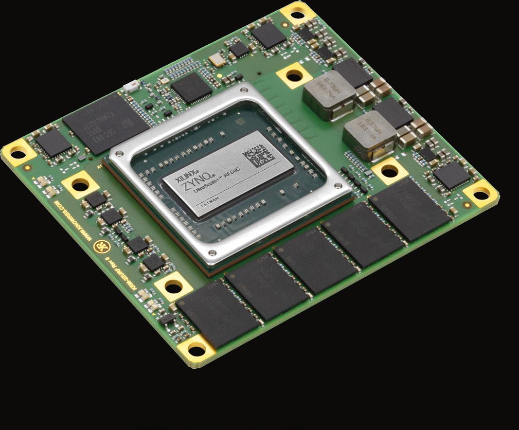
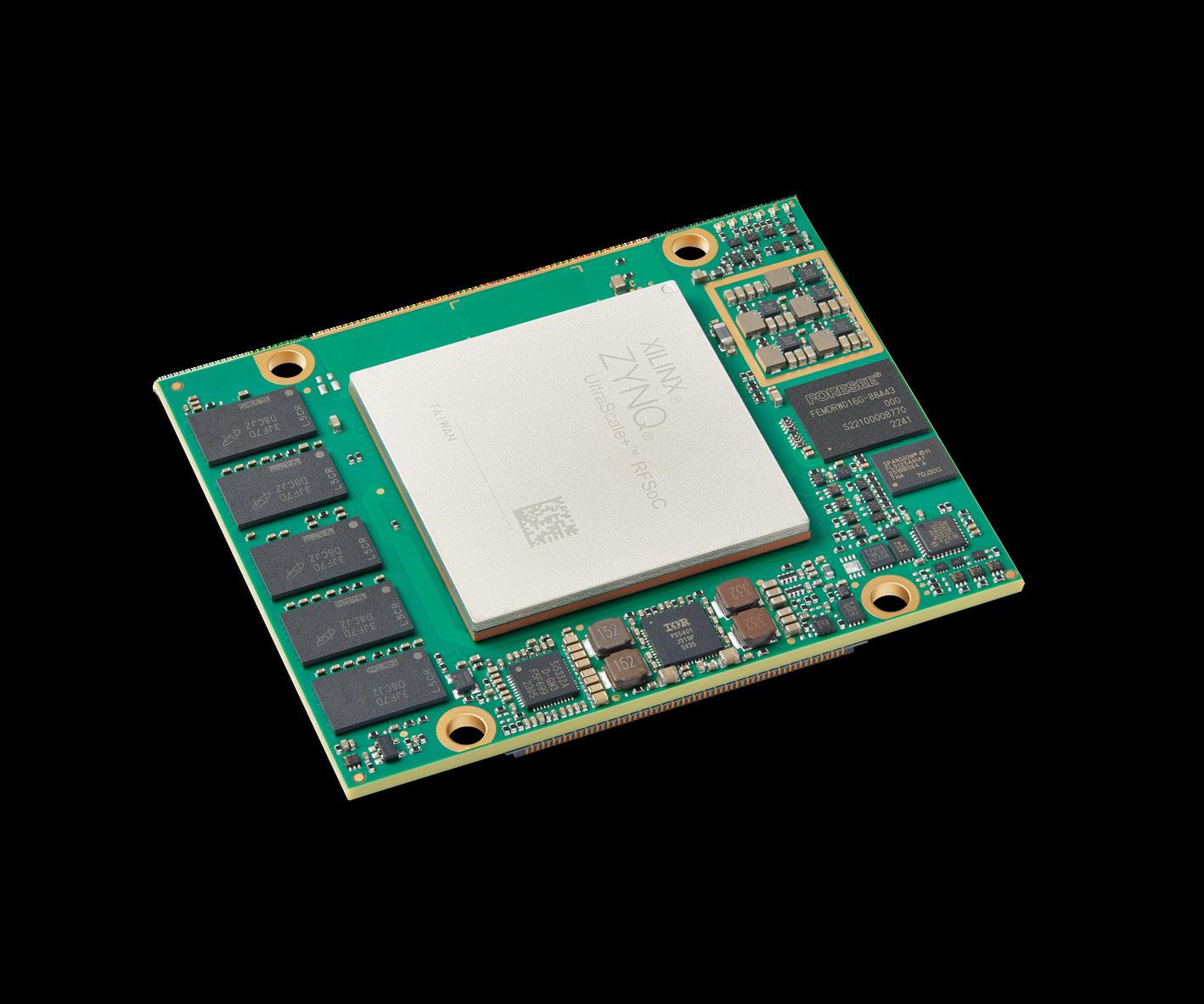
THE BROADEST RFSOM PORTFOLIO
• proven designs, shipping in volume since 2020
• ideal for communications systems, SIGINT, radar, T&M, and instrumentation of physics experiments
knowres com
Rethinking how we build highperformance
FPGA/ adaptive SoCs
Mike Rather, Sr. Manager Product Management, AMDD
High-performance FPGAs and adaptive SoCs increasingly need to be closely coupled with memory that can keep pace with evolving compute architectures. This is because a lot more is now expected of them. Each new FPGA generation adds more heterogenous compute capability, including upgraded programmable logic and DSP functionality. I/O bandwidth is also growing, with PCIe® Gen6, 100G and 600G Ethernet cores, as well as high-speed serial transceivers, which demand local highbandwidth memory for storage, buffering, and where necessary, SW application execution.
LPDDR5X is emerging as the preferred option in a wide range of applications from embedded applications to the datacenter, thanks to its high performance and lower power compared to DDR5. Yet this comes with multi-GHz signaling and tight Signal Integrity and Power Integrity (SI/PI) margins to ensure a robust solution. We can design these memories on the board to meet these challenges, but that comes with added complexity and cost.
Despite being capable of delivering higher bandwidth and lower power per bit, as well as offering significantly greater memory throughput and efficiency, the interface complexities of DDR5 and LPDDR5 are becoming factors that shape the rest of the system architecture. We have moved, almost by default, to a build-to-memory approach that constrains designs rather than optimizing them.
Exploring this constraint, the floorplan of FPGAs, along with I/O bank allocation, power domains, and even board stackups, are dictated by the DDR interface, rather than what the compute architecture actually needs. At the board level, SI/PI analysis is required for both pre- and post-layout, along with complex stackups and ultra high-density PCB design and manufacturing techniques; these drive cost and lead times. That’s a problem.
Security pressures add another layer. More systems are being deployed at the edge, and frameworks such as the Cyber Resilience Act (CRA) raise the bar for protecting data in flight and at rest. External memories expose a broad attack surface, and the combination of highspeed interfaces and exposed memory buses makes it harder to guarantee confidentiality and integrity across the platform.
At the same time, system-level footprints have become a hard constraint. Form factors are shrinking, and designs targeting VPX, PXI, or dense PCIe cards have little tolerance for the board area consumed by DDR devices. Memory placement and routing no longer just influence the board; they define the physical limits the entire system must fit within.
It’s time to think outside the box
The focus on system-level planning has traditionally guided FPGA design. But we are now seeing a shift toward tighter integration, where devicelevel considerations sit alongside the system view rather than beneath it. This isn’t done to replace the system perspective, but to free the device from the constraints imposed by DDRcentric architectures. What if the FPGA became the anchor point for this integration, rather than the board?
This kind of thinking opens the door to architectures where memory is placed to serve the FPGA, not the other way around. For example, this could bring high bandwidth memory physically closer to the fabric, eliminating the SI/PI, training, and routing constraints that dominate DDRbased designs. Shorter interconnects would also reduce latency and improve determinism for sensitive workloads and real-time systems. And the freed-up routing channels and simplified power domains would give more flexibility in how systems are designed. It could additionally enable compute, fabric, and I/O to scale without being limited.
For FPGA engineers, it could also reduce technical risk by removing those design and development stages now necessary. These changes could mitigate DDR-driven board stackups, tight length matching and impedance tuning, and multi-week SI/PI closure cycles. And, importantly, the bring-up issues and problems that can define early hardware validation, including the long debug cycles required to isolate whether faults lie in routing, signal or power integrity, or timing margins could be reduced.
This is where a Memory on Package (MoP) approach comes into the picture. If highbandwidth, low-latency memory is placed directly alongside the FPGA die, rather than outside of it, the existing constraints would be removed. If there’s no external DDR interface to route, there’s no SI/PI envelope to close.
With the memory integrated inside the package, it would also effectively remove the memory subsystem as an external attack surface. With no exposed DDR traces, sockets, or byte lanes, the memory path would become extremely difficult to probe, intercept, or tamper with. This would offer a significant advantage for edge-deployed systems and a solid foundation for meeting security requirements.
Instead of shaping the architecture around the memory interface, MoP would allow the architecture to be shaped around the compute again. This would restore the balance between the fabric, I/O, and memory, and enable devices to scale without the constraints imposed by traditional DDR-based designs.
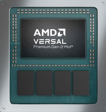
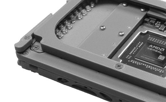
Fortunately, this is already happening. Take the new, industry-first AMD Versal™ Premium Gen 2 2VP3622 MoP as an example. Around the same size as a standard FPGA, it integrates 32 GB of LPDDR5X directly inside the package, enabling board sizes to be reduced by ~60%1, and designs to fit into PXI, 3U VPX, and PCIe form factors.
Fig. 1. The AMD Versal Premium Gen 2 2VP3622 MoP integrates 32 GB of LPDDR5X directly inside the package
By integrating the external DDR interface, the Versal Premium Gen 2 2VP3622 MoP allows the fabric, processing engines, and I/O to operate at their intended throughput without being gated by board-level signal integrity constraints. Because the LPDDR5 subsystem is integrated, it removes the high-speed memory interface, reducing SI/PI uncertainty, simplifying layouts, and cutting weeks to months from bring-up and validation.
The result is a predictable, factorycalibrated platform that delivers high bandwidth, lower latency, and consistent performance across temperatures and lifecycles. By doing so, it lowers technical risk and shortens development schedules, enabling teams to reach stable hardware and production-ready designs faster than traditional DDR-based architectures.
Now let’s think inside the box
AMD has explored this territory before with the Versal HBM adaptive SoC, which also integrates memory inside the package. However, it does so in a different way by vertically stacking DRAM dies, connecting them with through-siliconvias (TSVs), and mounting them on a silicon interposer. This delivers massive, multi-terabit per second bandwidth for memory-bound, compute-intensive workloads such as AI acceleration and HPC kernels. That maximum bandwidth does, though, come with trade-offs such as high thermal density, a limited temperature range, and a shorter product availability lifecycle.
This is where the Versal Premium Gen 2 2VP3622 MoP shines, with a fully integrated memory subsystem, a long operating life, industrial temperature robustness, and design simplicity.
What changes when memory moves inside the package
While HBM focuses on maximizing bandwidth, MoP devices address the board-level constraints that limit system performance. Integrating 32 GB of LPDDR5X inside the package removes the footprint and routing penalties of discrete memory devices, shrinking board sizes and freeing layouts that would otherwise be dominated by DDR placement.
With the memory subsystem on-package, the usual SI/PI issues associated with multi-gigabit DDR interfaces fall away, reducing technical uncertainty and making early hardware bring-up far more predictable by lowering risk. The shorter interconnects also improve LPDDR5X performance by removing the losses and conservative margins imposed by board-level routing and enabling much tighter coupling inside the package.
Eliminating long DDR traces removes a major source of EMI and signal degradation, while the package substrate enables much shorter, tightly controlled interconnects with lower parasitics than traditional PCB routing. The result is a high-performance memory solution with significant technical risk reduced.
And because the memory is no longer dictating placement, power domains, or stackups, MoP devices can be deployed cleanly into VPX and other constrained form factors where it was previously difficult to accommodate several highspeed external DDRs.
The architectural advantages of the Versal
Where MoP can make a real difference
The architectural advantages of the Versal Premium Gen 2 2VP3622 MoP translate directly to the kinds of systems that have been pushing hardest against the limits of external DDR.
High-performance networking platforms can take advantage of the connectivity provided by 600G Ethernet, PCIe Gen6, and high-speed transceivers without overwhelming external DRAM. The integrated LPDDR5 also provides the bandwidth and determinism needed for packet buffering, flow control, and real-time analytics.
In aerospace and defense, the on-package LPDDR5 improves security by eliminating exposed memory traces and reducing opportunities for physical probing. Tighter integration also supports established form factors such as VPX, enabling rugged and thermally-constrained designs.
While in test and measurement, the availability of 32 GB of integrated LPDDR5X memory inside the package supports deeper capture buffers and highrate data processing for oscilloscopes, analyzers, and instrumentation. High-performance PL and DSP blocks also interface cleanly with high-speed analog front ends, enabling more capable and compact equipment.
Similarly, real-time data-processing systems can take advantage of the predictable memory behavior and reduced board complexity, enabling designs that previously required multiple devices or larger form factors. The combination of integrated memory and high-performance I/O opens new possibilities for small-form-factor, power-efficient architectures.
All of these applications can also benefit from the time-to-market advantages of using Memory on Package devices. Starting with a performant, verified, working memory interface reduces the system design effort and can shorten the overall time to get products to market.
Footnote
1. Based on AMD internal measurements taken in April 2026, of the board area of a Versal Premium Series Gen 2 MoP 2VP3622 adaptive SoC, compared to the board area of a Versal Premium Series Gen 2 monolithic adaptive SoC with external memory. (VER-111)
Taken together, these capabilities mark a shift in how high-performance FPGA systems can be architected. By removing long-standing DDR constraints, MoP frees FPGA engineers to design what’s needed without restrictions, reduces technical risk, and provides a stable foundation for long lifecycle, industrial temperature deployments. For teams facing rising bandwidth demands and shrinking form factors, it offers a practical and forward-looking path.
Migrating from a legacy FPGA to a modern scalable platform
Rachael Peterson, Design Authority, Principal Engineer, Concurrent Technologies Plc
FPGA designs that met the requirements and technologies of ten years ago and more are now increasingly becoming legacy devices. While they still work, they’re now constrained by dated architectures, older clocking primitives, and limited DSP blocks. Interfaces like PCIe, DDR4 and DDR5, and multi gigabit transceivers are also often not fully supported.
At the same time, toolchains have moved on and integration complexity has increased, with Arm cores, hardened memory controllers, and high speed I/O. Designs that once required only small updates now need more substantial changes just to stay compatible with new processors and board-level requirements.
At Concurrent, for example, we design and manufacture Intel processor-based embedded computing cards and chassis systems. Our cards contain an Intel Xeon or Core CPU, depending on the target application, along with DRAM, storage, Ethernet and PCIe interfaces, and usually I/O such as USB or display interfaces.
The core logic that controls the power to the CPU, brings it out of reset, and enables it to communicate with and control other board functions is contained within an FPGA. For many years this has been implemented with a Microchip ProASIC3 FPGA, and the core logic and functionality have been migrated from product to product and adapted as necessary for each new platform.
In addition, there is usually a secondary processing element we use for the Intelligent Platform Management Interface (IPMI). This is typically implemented using a small microcontroller such as an STM32.
This has worked well as a core architecture and supported the development of many platforms over the years. However, it has limitations and the CPU platform is evolving beyond what we can easily and cleanly support within the existing design.
Legacy platform realities: ProASIC3 at its limits
The ProASIC3 has been around for almost 20 years. It’s a solid performer with flexible I/O, a reasonably sized FPGA fabric with dedicated FIFO logic for the RAM blocks, Flash-based instant-on operation, and low power. These are all things which made it a good choice when it was first selected.
However, the minimum I/O bank voltage is 1.5V which limits its ability to support the I/O standards at lower voltages that are becoming more common on devices we need it to interface with. The number of available I/O pins is also constrained, so we’re pin-bound in the parts we currently use. There are solutions that would have allowed us to continue with ProASIC3 for a little longer, like level translation, I/O expanders, etc, and these still have their place today. That said, we needed to consider the bigger picture and our long-term vision and strategy, not just Can we make it work today?
In order to develop our products and bring new functionality to the market, our FPGA platform needs to be able to support the needs of tomorrow as well as those of today. ProASIC3 will stop being able to support those needs as CPU technology and platform requirements move on, so we sought to identify a solution which could grow with the product roadmap.
New Intel architecture as the forcing function
In the Xeon CPU generation we were targeting, Intel has moved to a CPU-centric architecture where the traditional Platform Controller Hub (PCH) no longer exists in its own right. Instead, critical parts are embedded within the CPU itself, with boot sequencing and hardware initialization handled within the microcode of the System-on-Chip (SoC). This has knock-on effects for the power sequencing logic, I/O voltage compatibility, and required supporting functions.
These changes were going to have a deeper impact on the FPGA platform and transform the process from just copying what we’ve done before and tweaking a few bits to make it fit, to rewriting large chunks of the core functionality. This increased risk significantly and amplified any technical debt because more needed to be reopened and changed.
Ultimately, as the Design Authority for the platform, I needed to address the risks to the technical feasibility and schedule, while also factoring in future outcomes. The decision was made that the risk-reward ratio improved significantly if we migrated to a new platform, and this was the lowest risk option.
Selecting a modern FPGA platform
We needed to migrate to a new platform to enable easier interfacing with new CPU generations and enable our FPGA designs to scale for new functionality. There was a large selection of possible choices from a number of vendors, so the question became how to narrow this down to a vendor and eventually a part.
In order to support an increasing role for FPGAs beyond board support logic, the final choice had to be more than the same again with better I/O. We needed a platform designed to scale to much bigger applications, with a large ecosystem of solutions and available IP.
There were four main FPGA vendors to choose from: AMD (Xilinx), Intel (Altera), Microchip Technologies Inc. (Actel), and Lattice Semiconductor. While all four vendors have scalable solutions, AMD and Intel offered the broadest ecosystem and tool maturity for our requirements, which helped narrow the field.
The final choice was to identify parts which would work within the current target application and to narrow down the options. The combination of available board area and I/O count helped with selecting the suitable candidates. Combining this with the extent of the support ecosystem, the AMD Artix-7 family was chosen as the solution.
Platform strategy: Artix-7 as a stepping stone
The AMD Artix-7 offers many new architectural improvements but was never intended to be the final destination. It doesn’t solve one key issue, namely that the new CPU architecture moves away from the 1.8V I/O interface standard for key signals to much lower voltages of 1.0V and 1.1V for many signals.
To solve this, we needed to include I/O level translators to match the FPGA I/O voltages to the CPU I/O voltages. This comes at the cost of additional interfacing complexity, board real estate, and Bill of Materials (BOM) cost.
In addition, the board space constraints limited the package size and I/O count. This meant that in order to interface to a number of external devices we needed to include I/O expanders connected to the FPGA via I2C. Much like the I/O level translators, these have penalties, including the complexity of interfacing to the I/O expanders.
The solution to this would be to migrate from the Artix-7 to the Spartan UltraScale+ for our next platforms. This supports lower I/O bank voltages so we could directly interface to the CPU. It also has much more I/O in a smaller footprint so we wouldn’t need the I/O expanders.
We’d done the hard part of migrating to the AMD ecosystem already. The next stepping stone was to optimize for a simpler and more flexible solution to take us into the future. We didn’t just go straight to the Spartan UltraScale+, however. It’s a very new device from AMD and is only just starting to get a proper public release. Our project was slightly too far ahead of the launch to take advantage of it, so we used the Artix-7 as the ideal first step.
Architectural and debug capabilities unlocked
The Artix-7 family enabled us to immediately scale up what the FPGA does within our platform. The Board Support FPGA can be a complete platform in its own right, there to add system functionality, no longer just board support logic. We had the ability to include soft core processing (Microblaze V), interface to DDR3 SDRAM, create complex systems visually within the Block Design functionality of Vivado, and drop in standard IP from their extensive library which all connect together using the ubiquitous AXI interface. This enabled us to make significant architectural changes to improve the core platform.
As mentioned, we usually have a separate microcontroller for our IPMI functionality. Because of the greater capabilities of the new FPGA platform, we incorporated this within our FPGA design using a Microblaze V, enabling tighter coupling between the IPMI and CPU subsystems. We also added a second Microblaze V to provide additional board management functionality, giving much more insight into and control over the operation of the FPGA via one of the USB serial interfaces the new platform provides.
Development and debugging capability are where the new solution really shines though. We built the JTAG programmer and debug serial interfaces directly into the board using an FTDI USB serial device and these integrate tightly with AMD Vivado/Vitis so we now have one solution for programming the FPGA and the microcontrollers, all tied together with a neat little bow.
We were also able to leverage the Integrated Logic Analyzer (ILA) and Virtual I/O (VIO) functionality of Vivado to gain greater insights into where issues are occurring so they can be identified and fixed much more quickly.
A good example of the debug capability in action was getting our new Enhanced Serial Peripheral Interface (eSPI) IP block up and running. We could capture and decode the eSPI transactions on our oscilloscope but we couldn’t see from there the reason it was failing. After inserting an ILA on the eSPI block we were able to track down where it was getting stuck and the missing response. This enabled us to quickly find a solution and move on to the next step.
Similarly, when debugging the power sequencing of the rails for the new CPU we were able to use the ILA to provide insights into where things were stopping in the power-up process, and we were able to use the VIO to override the sequencer and enable each of the rails to test they were working.
The foundations have now been laid for our future FPGA developments. We have a scalable architecture with a large existing ecosystem we can leverage. We’ve got debug tools baked right in to eliminate the need for external programming tools. We have tighter coupling between various parts of our design, and hardware and software teams are now working within a familiar shared environment for easier collaboration.
Possibly the most important benefit for the long term is that it will allow us to scale up for future designs which are more FPGA-focused rather than CPU-focused, and this is where things will start to get interesting. For now, reusing the FPGA designs between projects is simpler and more maintainable, reducing design effort. The Board Support FPGA has become a well-defined platform in its own right, there to complement the CPU and provide additional functionality, not just to help the CPU to boot.
What surprised us:
Building a new FPGA platform was easier than expected
After deciding to take the leap and go ahead with a major step change in our FPGA architecture and capability, stakeholders quite rightly challenged the risks this could introduce both to the development lifecycle and in the product design where the change was being introduced. By using objective success criteria and early proof-ofconcept (PoC) work, we found the risks were manageable and the benefits compelling.
We approached the migration as a structured engineering change. We aligned on the ‘why’, agreed measurable acceptance criteria, ran early PoC activity, and then scaled the approach once confidence was established.
In the end though, implementing the new FPGA platform was surprisingly easy. There is a plethora of development boards available for most FPGAs and the Artix-7 is no exception. These come as self-contained development platforms with example FPGA and software designs to get FPGA and software engineers up and running quickly, as well as schematics and layout details for the board designers to use. We chose an Arty A7 and used the supplied schematics as the basis for our own, ensuring things like FPGA configuration, clocking, and DDR3 interfaces would be correct from the outset.
We had anticipated there would be challenges faced when making the architectural shift. In the end, this change was much easier than expected and the FPGA platform worked straight away and provided immediate benefits in debug visibility and development flow. That, in turn, reduced integration uncertainty elsewhere in the program and helped build confidence in the longer-term platform strategy.
Tooling and workflow: Where ambition got ahead of us
We also used the migration as a catalyst to improve build automation and reproducibility. Our first iteration aimed for a full CI/CD pipeline with ambitious goals. It delivered value, but we learned that FPGA workflows have different constraints (tool runtimes, licensing, artifact sizes and iteration cadence) and need a tailored approach.
We built a sophisticated CI/CD system, but it was optimized for software-style workflows. When hardware engineers started to use it, they found the setup and user experience added friction to day-to-day iteration. When errors occurred, we also learned we needed clearer ownership and support pathways to avoid over-dependence on a single team.
In practice, adoption lagged because the workflow added steps for rapid prototyping. We therefore simplified the path from change to bitstream for day-to-day engineering, and we’re iterating on automation with the hardware team so it delivers value without slowing iteration.
The key take-away here is not that CI/CD isn’t suitable for FPGA development. It is, but it can be complicated and you need to bring your hardware team along for the journey, building on the opportunity to do things correctly for the long term.
Results and outcomes
We now have a new, extensible FPGA platform fit for the future. It offers more capability and scalability, improved development tools, and better debug tools with programming and debug interfaces baked into the architecture. This has enabled us to more rapidly analyze and debug issues as we face them, speeding up development times considerably.
With the previous FPGA, the tools were limited so when something didn’t work we had to figure out how we could get the data we needed to solve the problem, relying heavily on simulation and trying to reproduce the failure as a test case in the testbench. Now we add the signals of interest to an ILA and in a matter of minutes we can start debugging live on the real hardware where the problem actually exists.
Future projects now have a powerful platform to build upon as we look further ahead to where we want to be, not just the next project.
Conclusion: Advice to teams considering a similar move
If you’re considering whether you should embark on a similar path, start by being clear about the driver. What is changing in your platform or requirements that makes maintaining the status quo more complex or riskier?
To give due diligence to the decision, evaluate whether you’re carrying any technical debt within your legacy architecture that is quietly sapping productivity, slowing down development, making debug harder. These factors can quietly add cost and time over multiple programmes.
Look at whether the benefits of future-proofing your architecture, reducing or eliminating technical debt, and introducing tighter integration of components within the subsystem, better development environments, and better debug capability are worth the extra development effort now. That’s not to say this isn’t without risk, but you can mitigate many of the risks associated with change, and weigh those that remain against the benefits you’ll gain.
Ultimately, the benefits for us have been significant, and made what was a very challenging project a lot more manageable because the FPGA subsystem was much more flexible and manageable.
Validating your FPGA design: The role of post-layout signal integrity
Dan Binnun, Founder, E3 Designers
Post-layout signal integrity is the process of validating that the physical implementation of a PCB supports the performance your system requires and was designed for. Many engineering teams take a reactive approach to signal integrity and this will be the first step they take in the process. Whether or not you perform pre-layout signal integrity, it’s the final opportunity to catch any issues before fabrication, and the significant risks of skipping it become crystal clear.
The primary goal is to verify that the design intent has been successfully implemented and that no issues were introduced during the PCB placement and routing processes. This verification approach typically unfolds in stages, moving from broad automated checks of the entire board to highly detailed, fullchannel validation of the most critical links.
Impedance and crosstalk scans
One of my favorite types of post-layout simulation and analysis is to perform automated scans of the entire board (or a subset of traces of interest) for impedance discontinuities and potential crosstalk violations. Electronic Design Automation (EDA) tools like Ansys SIwave make these scans relatively simple to set up, simulate and analyze. What I really love about these scans is that they act as powerful fresh eyes for the PCB layout and signal integrity engineering teams, systematically combing through every trace of interest on the PCB. Their value lies in their speed and comprehensive nature: the scans can quickly identify implementation mistakes or overlooked issues that are difficult to catch in a manual review.
Often, these scans flag problems that seem obvious after the fact. Perhaps a trace was accidentally routed with the wrong width, or a differential pair was routed with the incorrect traceto-trace spacing, or a signal trace unexpectedly crosses a split or void in a reference plane. These are precisely the kinds of errors that can easily creep into a complex design but can be catastrophic to signal integrity. When you have been working on a PCB layout for an extended period of time, these issues are far too easy to overlook due to design fatigue. Luckily, the EDA tool doesn’t have the same affliction, and can help us see things we might otherwise miss.
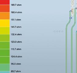
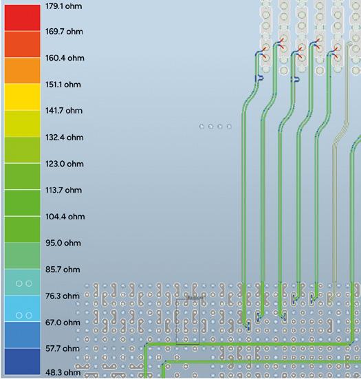
Impedance scans analyze the geometry of each trace of interest in relation to its reference plane(s) to calculate its characteristic impedance. The tool then generates a board-wide plot, color-coding any trace that deviates from its target impedance (e.g., 50 Ω single-ended or 100 Ω differential) beyond a specified tolerance. This provides a very easy-to-digest visual report on the impedance control of the entire design.
Crosstalk scans identify potential ‘aggressor’ nets that are likely to couple noise onto adjacent potential ‘victim’ nets. The analysis flags areas where traces run in parallel for too long, or too close together. In Ansys SIwave specifically, generic driver models are used to facilitate a quick analysis and provide prompt feedback, without requiring overly detailed and specific model assignments to potentially thousands of nets on a PCB.
It is important to note that this methodology is not a suitable replacement for the rigorous crosstalk analysis required in high-performance RF systems, which typically demand a full 3D EM solver that can account for all physical geometry including shielding, connectors, and the board enclosure to accurately predict electromagnetic coupling. These automated scans are a powerful tool for general analysis of PCB layout, not a onesize-fits-all solution for crosstalk analysis.
It’s also important to understand the limitations of these scans. Because they do not utilize 3D EM solvers, their accuracy is limited to a certain frequency range. However, they remain an indispensable part of the verification process, capable of catching a wide array of common layout issues. Performing these scans should be standard practice for any modern digital design, as they allow engineers to quickly pinpoint and evaluate potential problems before committing to more time-consuming, full-wave simulations.
S-parameter extraction
After performing board-wide scans, it can often be beneficial to look at a specific representative channel for each major interface type we have routed. The hope here is that the high-speed interconnect has been routed with consistent structures, spacing and methodology, whether through proactive planning or disciplined layout practice. This means we can make a reasonably sound correlation between the performance of a representative channel, perhaps a single lane of a PCIe x16 interface, and the other lanes within that complete interface.
This is accomplished through S-parameter extraction, a process where we convert the physical geometry of routed traces into a proven and highly accurate behavioral model that describes how that geometry affects a signal. The process begins by identifying the nets of interest in the layout and defining ports at their start and end points on our PCB, like the pads of the FPGA, SoC or ASIC footprint and a connector or another partner device. These ports act as the virtual measurement points for our simulations.
Modern EDA tools like Ansys SIwave, Ansys Electronics Desktop, and Siemens HyperLynx are then able to employ powerful hybrid solvers to combine the speed of 2.5D solvers for uniform trace sections (microstrip and stripline routing) with the higher accuracy of full-wave EM solvers for complex 3D geometries like transition vias and BGA breakouts. This approach provides a highly accurate S-parameter model without the prohibitive simulation time of a full 3D solution for an entire PCB.
Once extracted, this ‘as-routed’ S-parameter model can be used in two critical ways.
Standalone interconnect assessment
We can analyze the S-parameter model as a standalone entity to verify its compliance against specific performance targets. This is particularly useful for standardized interfaces that have this type of metric defined in their standards and specifications. The PCI Express specification, for example, defines a return loss target for each segment of the channel. By extracting the S-parameter model of our routed PCB, we can directly compare its return loss against the PCIe specification. This provides a clear pass/fail assessment of that specific segment, allowing us to confirm compliance or identify issues without needing to simulate the entire end-to-end channel.
Fig 1: A visual report of impedance scans using Ansys SIwave
Full-channel simulation
The other way we can utilize the S-parameters is to use the extracted model to evaluate how the routed interconnect performs as part of the complete system. In many workflows, early simulations when they are performed rely on proxy models and we can now replace them with the S-parameter model of the actual, physically routed interconnect.
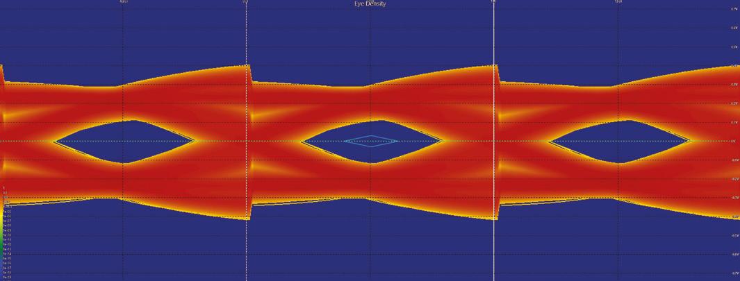
By running a full-channel simulation with our ‘as-routed’ data, we can quantify the impact of the physical layout on our design margins. The ideal scenario is one that ends with a full-channel simulation that shows sufficient margins against whatever metrics may be of interest (e.g., COM, insertion loss, return loss, eye-mask measurements or bit-error rate (BER) measurements). While the true pass/fail test is always the physical hardware, a positive result in this final simulation serves as the most comprehensive virtual sign-off possible. It provides the final, data-driven confidence needed to commit the design to fabrication.
Over to you
Post-layout signal integrity analysis plays a decisive role in ensuring a high-speed design performs as intended. By combining automated board-wide scans, accurate S-parameter extraction and full-channel simulation, it gives engineers a clear understanding of how the routed interconnect behaves under real operating conditions.
This structured approach transforms post-layout signal integrity from a last-minute check into a disciplined verification stage. It allows teams to uncover layout issues that are difficult to detect manually, validate compliance against interface standards, and quantify system-level performance before fabrication. The result is a more predictable design process, reduced risk of costly re-spins and a higher degree of confidence in the final implementation.
For many engineering teams, post-layout signal integrity analysis has been sufficient. As modern FPGAs increase density and pin counts, manage higher speed signals, and integrate with other technologies, teams are now turning to pre-layout signal integrity as well.
They’re front-loading the signal integrity engineering effort by diligently selecting components, engineering a robust stackup, simulating system-level performance with mock-up channels, and creating a library of pre-validated, high-performance building blocks.
The goal is no longer to discover if the design works, but to confirm that it does, turning the final simulation into the true stamp of approval every team hopes for.
Want to find out more? Read Dan Binnun’s article, ‘Avoiding costly respins: The case for pre-layout signal integrity’, in Issue 2 of the FPGA Horizons Journal online
Fig 2: An eye diagram showing BER with Siemens HyperLynx
Kevin Hubbard, Black Mesa Labs
Modern Electronic Design Automation (EDA) workflows typically generate an overwhelming amount of data. Even a single FPGA or ASIC place-and-route run can easily produce tens to hundreds of megabytes of timing reports, congestion maps, Design Rule Check (DRC) logs, synthesis summaries, and tool-specific diagnostics, each packed with thousands of lines of dense, highly structured text.
Engineers routinely sift through multi-megabyte Static Timing Analysis (STA) reports, sprawling RTL hierarchies, and vendor-specific output formats just to answer simple questions like What failed?, Where is the bottleneck?, or Why did timing suddenly collapse? These files are often too large to read manually and too irregular for simple grep operations.
All of which leaves developers spending hours using tools that were never designed for this scale or complexity, scrolling and cross referencing reports to extract the handful of insights needed to move a project forward.
Fortunately, there is another way.
Ash (eda_ai_assist) is a command-line AI assistant for FPGA and electrical engineers, built with an intentional, minimalist philosophy. It’s not trying to be a generic chatbot, it’s a precise command-line tool much like grep, but with AI intelligence. It speaks the language of electrical engineers and stays out of the way until invoked.
Ash allows engineers to ask natural-language questions and get precise, context-aware answers, even when the underlying files are enormous. Instead of scrolling through thousands of lines of tool output, engineers can finally interrogate their data directly and let Ash do the heavy lifting.
Ash and grep both run from the command line and operate on the massive text files common in EDA workflows like netlists, timing reports, synthesis logs, and more. But while grep is limited to strict pattern matching, Ash accepts natural-language questions and interprets what the engineer is actually trying to find.
The grep command is excellent for locating specific strings. Ash excels at understanding what those strings mean in the context of the design. It brings intelligence to EDA workflows without changing how engineers work, by introducing a different way of using the command line:
%grep ERROR synthesis.log
%ash summarize the errors in file synthesis.log and sort by severity
Getting started with Ash
To use Ash, you need a modern Python environment on a Linux, Unix, Windows, or macOS computer. You also need an API subscription to one or more AI cloud LLMs from vendors like Amazon, Microsoft, or Google.
A cloud subscription typically involves submitting a credit card in exchange for an API_KEY. Don’t worry, however. AI subscriptions are more like utility bills than streaming services: you only pay for what you use, with no monthly minimum charge.
Now, download the Ash command-line script, eda_ ai_assist.py, from the author’s GitHub at https:// github.com/blackmesalabs/eda_ai_assist.
Using your shell’s environment variables, you can then configure Ash to talk to your LLM provider. Note that the syntax varies slightly between Bash, CSH, and PowerShell. A Bash configuration file for use with Gemini, for example, would be:
export ASH_DIR="$HOME/.ash" export ASH_API_KEY="mykey123" export ASH_PROVIDER="gemini" export ASH_MODEL="gemini-2.0-flash" alias ash="$ASH_DIR/eda_ai_assist.py"
The ASH_DIR directory may be used to store the program itself as well as any optional configuration files.
USING ASH IN CLI ONE-SHOT MODE
The most basic way to use Ash is CLI one-shot mode. In this mode, Ash behaves like any other command-line utility, very much in the spirit of grep. You invoke the tool, pass it a question or instruction, and Ash returns a direct answer. There’s no session state, and no chat history. It’s ideal for quick queries, automation, and shell scripts where you want a single prompt in and a single result out.
Note the use of the keyword file in Example 1 below, which instructs Ash to upload a valid filename to the cloud for analysis. Similarly, using the phrase output to <filename> would tell Ash to write its result to a new file named <filename> instead of sending it to STDOUT.
In the second example, Ash correctly identifies Hsync and Vsync as VGA signals, even though ‘VGA’ does not appear in their signal names. Let’s see grep try to do that.
Example 1
Example 2
%ash tell me the pins for all the VGA signals in file post_route_io.rpt
The VGA signals and their corresponding pins are:
* vgaGreen[3]: D17
* vgaGreen[2]: G17
* vgaRed[0]: G19
* vgaGreen[1]: H17
* vgaRed[1]: H19
* vgaGreen[0]: J17
* vgaBlue[3]: J18
* vgaRed[2]: J19
* vgaBlue[2]: K18
* vgaBlue[1]: L18
* vgaBlue[0]: N18
* vgaRed[3]: N19
* Hsync: P19
* Vsync: R19
%ash what is the worst timing path in file post_route_timing_summary.rpt ?
The worst timing path in the file post_route_timing_summary.rpt is:
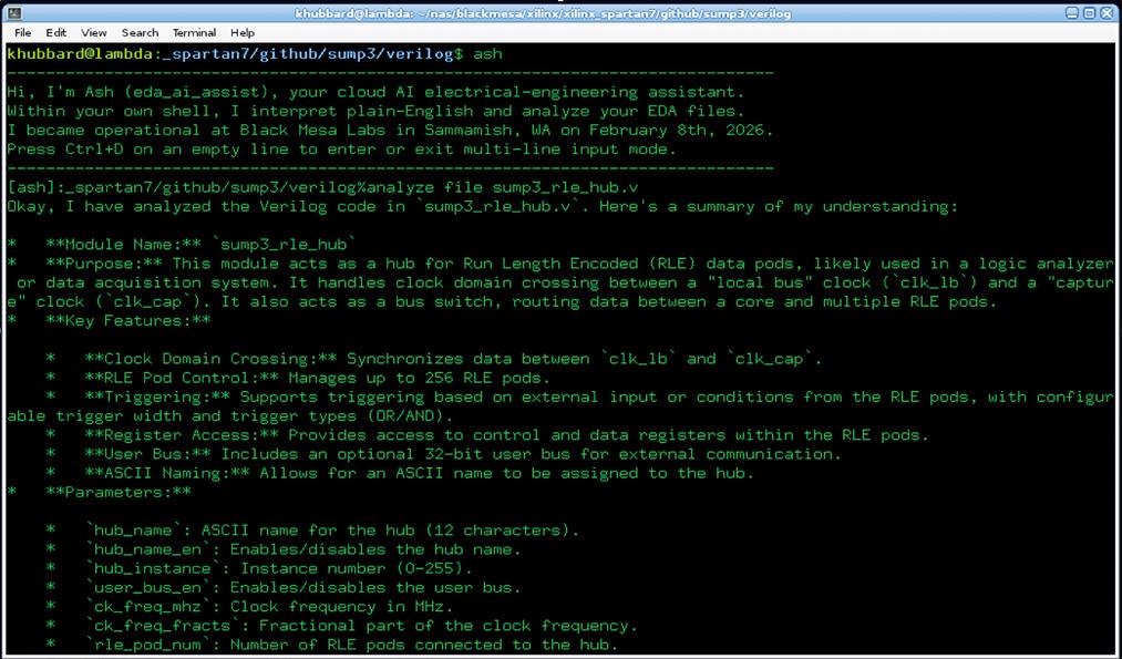
In interactive mode, Ash runs as a lightweight wrapper around the user’s existing shell, adding AI intelligence without replacing familiar workflows. Every command you type, whether it’s a shell command, an AI question, or a mix of both, becomes part of a running session with full history. This makes it easy to refine questions, compare results, and build on previous context just as you would in a chat environment, but without ever leaving the terminal.
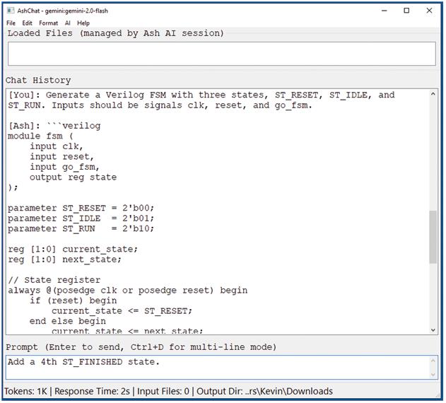
Interactive mode is ideal for longer debugging sessions or exploratory analysis, giving engineers a conversational layer on top of their real shell while keeping all the power of their native environment intact. In the following screenshot example, Ash is launched from the Linux command line in interactive mode and then a conversation is started from the CLI prompt.
In this next example, Ash maintains a conversation across multiple prompts while still allowing regular shell commands to run alongside it:
[ash]:%list the VGA signals in file post_route_io.rpt
Analyzing file post_route_io.rpt, here are the VGA signals:
* Hsync
* Vsync
* vgaRed\[3:0]
* vgaGreen\[3:0]
* vgaBlue\[3:0]
[ash]:%what are their voltage levels and drive strengths?
Analyzing the file post_route_io.rpt, here’s the voltage levels and drive strengths of the VGA signals:
| Signal | Voltage | Drive (mA) |
| Hsync | 3.30 | 12 |
| Vsync | 3.30 | 12 |
| vgaRed\[3:0] | 3.30 | 12 |
| vgaGreen\[3:0]| 3.30 | 12 |
| vgaBlue\[3:0] | 3.30 | 12 |
[ash]:%ls -l
-rwxr-xr-x 1 khubbard khubbard 73831 May 3 2025 post_route_io.rpt
-rwxr-xr-x 1 khubbard khubbard 9112 May 3 2025 post_route_pwr.rpt
-rwxr-xr-x 1 khubbard khubbard 2970 Oct 20 2024 post_route_timing_check.rpt
-rwxr-xr-x 1 khubbard khubbard 31385 May 3 2025 post_route_timing_summary.rpt
AshChat is the GUI-based companion interface for Ash, designed for users who want the intelligence and engineering focus of Ash without living inside a terminal session. It brings Ash’s reasoning engine, personality, and multi-provider backend into a clean, modern chat UI. Think of it as Ash’s conversational surface, while the CLI remains its precision instrument.
AshChat communicates with Ash through its public API interface, acting as a clean, GUI-based front end. All the intelligence, routing logic, and provider selection still happen inside Ash itself. AshChat simply sends requests through the API and displays the results in a more relaxed, conversational environment. In that sense, AshChat isn’t a separate product at all, but a different doorway into the same core system.
USING ASH IN ENTERPRISES
Ash is engineered to support enterprise environments, where access control and auditability matter just as much as raw capability. Instead of distributing raw API keys to every engineer, Ash employs a user-token system in which each user receives an encrypted, per-identity token derived from a single site-wide API_KEY.
The real API_KEY never leaves the administrator’s hands: users only receive a cryptographically-bound token that Ash can decrypt and verify at runtime. This gives enterprises centralized control over credential rotation, per-user authorization, and usage tracking without exposing sensitive keys across the organization. Combined with Ash’s transparent logging and multi-provider backend, the token system makes Ash behave like a tool designed for serious, policy-driven engineering teams.
To create user tokens, the admin establishes an $ASH_DIR/site_key.txt file containing a site key. From there, they can generate user tokens using the secret API_KEY and the user account names, by invoking the ash_token_maker.py command:
While the Ash command-line program itself is free and open-source, there is a small cost because it uses cloud-based AI LLMs. These are billed like utilities, based on the number of input and output tokens. For example, the author used Anthropic’s Claude LLM to build the AshChat GUI front end, and after a couple of weekends of development, the total Amazon AWS bill was just under US$10.
Where to go next with Ash
The Ash API makes it easy to add AI capabilities to any Python application. After importing the Ash module, you simply open a new LLM session, ask a question, and read the response. For example, Black Mesa Labs’ Sump3 ILA uses the Ash API to perform tasks such as counting signal transitions between cursors. The following example shows a typical hello world demonstration of how straightforward it is:
hello_world.py from eda_ai_assist import api_eda_ai_assist ai = ai.open_ai_session() api_eda_ai_assist() rts = ai.ask_ai("What do starter programs say to the World?") print(rts)
CONCLUSION
Ash makes it easy to work with the massive text files produced by modern EDA tools. Instead of digging through reports or building complex grep scripts, engineers can ask direct questions and get clear answers. Whether used from the CLI, in interactive mode, or through the AshChat GUI, Ash adds intelligence to existing workflows without changing how engineers work. It’s a lightweight, open-source tool that turns overwhelming data into useful insights.
PRODUCTS PER APPLICTION GUIDE
ONE PLATFORM. EVERY APPLICATION.
SWISS-ENGINEERED FPGA & MLSoC MODULES MATCHED TO YOUR DOMAIN.
From satellite radar and surgical robotics to edge AI and real-time industrial control, Enclustra's modular SoM ecosystem gives your team a proven, production-ready FPGA foundation, so you can focus on the innovation that matters.
Vendor-independent SoC Modules matched to your domain, delivered faster.
Hidden verification errors and how UVVM finds them
Marius Elvegård, Senior FPGA developer and UVVM Steering Group Member, Inventas
UVVM (Universal VHDL Verification Methodology) has over the years established itself as a practical and scalable verification methodology for VHDL-based FPGA designs. It combines well-known verification concepts with a lightweight structure that fits naturally into typical FPGA development flows.
However, in recent years, increasing design complexity and higher demands on verification quality have exposed some recurring challenges in traditional testbenches. These include inconsistent use of assertions, limited visibility of unintended behavior, uncertainty around when verification is actually complete, and the complexity of testbenches themselves.
Over the past two years, UVVM has therefore been extended with several new capabilities aimed at improving robustness, predictability, and structure in larger verification environments. These additions focus on assertions, the detection of unexpected activity, completion detection, and simplified testbench setup through new context files.
Ensuring assertions don’t become afterthoughts
Assertions are a well-established verification mechanism in VHDL and are commonly used to express assumptions, constraints, and expected behavior directly in code. A traditional assertion checks that a condition holds at a given point in time and reports a message if it does not.
While powerful, such assertions are typically isolated: they report directly to the simulator and are not naturally connected to the rest of the verification environment. In larger testbenches this often leads to inconsistent behavior. Some checks stop simulation, others do not, some produce large amounts of log output and others are easy to miss. As a consequence, handling assertion results consistently across simulations and regression runs becomes difficult, and errors creep in.
UVVM Assertions address this by integrating assertions directly into the UVVM logging and alert handling infrastructure. Instead of producing standalone simulator messages, UVVM Assertions report through the same alert system as the rest of UVVM. Assertion violations are treated like any other verification alert and contribute to the same alert counters and summaries.
This gives the testbench full control over how assertion violations are handled, and users can decide whether an assertion should stop simulation, how many times it should be reported, and at what severity level. Logging behavior can be configured to report every occurrence or only the first, making it easy to confirm that an assertion is active without flooding the log.
Value-based assertions
Value / range checks
One-hot / encoding checks
Stable / change detection
Sequence & pattern assertions
Bit / vector propagation
Signal relationship checks
Uses standard UVVM alert levels
Included in alert summaries & counters
Control and reporting
Simulation stop controlled by alert threshold
Window & timing assertions
Event must occur within N cycles
Signal stable during window
Timeout detection
Pipelined windows
Logging on every hit or first hit only
Enable / disable
UVVM Assertions cover the most common assertion use cases seen in real FPGA designs. These include value-based checks, such as range checks and encoding checks, sequence and pattern checks for signal relationships over time, and window-based assertions that verify behavior within defined timing boundaries. Window-based assertions make it possible to express requirements such as response deadlines, stability during transactions, and timeouts in a clear and readable way.
Assertions can be used both in testbench code and in synthesizable RTL. When used in design code, they can be enclosed in standard translate_off / translate_on pragmas, ensuring that they are active during simulation but excluded from synthesis.
The main benefit of UVVM Assertions is not that they replace traditional assertions, but that they make assertions a natural and fully integrated part of the verification environment. This leads to cleaner logs, clearer summaries, and results that are easier to interpret and trust.
Finding the ghosts in the machine
Most testbenches focus on verifying what happens when a stimulus is applied to the Device Under Test (DUT). What is often left unchecked is what happens when no stimulus is applied. In many FPGA designs, interfaces are expected to remain idle for long periods of time, and unexpected activity during these periods can indicate design errors.
Traditional Bus Functional Models (BFMs) and VHDL Verification Components (VVCs) are very effective at verifying transactions initiated by the testbench, but they do not detect cases where the DUT generates interface activity on its own. As a result, unintended reads, writes, or signal transitions may go unnoticed, as shown in figure 2:
Fig. 1. UVVM provides a focused set of assertion types
Fig. 2. During periods without stimulus, unexpected interface activity may occur without being detected by traditional stimulusdriven checks.covering value checks, signal relationships over time,
UVVM’s detection of unexpected activity addresses this directly. When a VVC becomes inactive, it automatically starts monitoring the associated DUT interface, and if the DUT generates activity while the VVC is idle, an alert is raised through the standard UVVM alert system. Unwanted activity is therefore handled in the same consistent way as other verification errors.
This mechanism is particularly useful for detecting spurious transactions or control logic that activates interfaces at the wrong time. These issues are almost impossible to catch using stimulus-driven checks alone, but they become immediately visible when unexpected activity detection is enabled.
The severity level for unwanted activity is configurable per VVC and can be controlled directly from the testbench. This makes it possible to adapt behavior to different verification phases, for example treating unwanted activity as a warning during bringup and as an error during regression testing. The feature can also be disabled when required, such as in shared-bus scenarios where only one interface is expected to be active at a time.
Establishing the finish line
Stopping stimuli in a structured verification environment is usually straightforward, but determining when the verification is actually finished is often less clear. In testbenches with multiple VVCs and scoreboards, a simulation may appear to be complete even though there are still pending commands or unchecked expected values.
In practice, this uncertainty can hide real verification issues. Developers can compensate with fixed delays or manual end of test logic, but these workarounds are easy to get wrong and make it harder to trust that the verification environment has actually completed.
UVVM completion detection provides a reliable mechanism for determining when a UVVM-based testbench has truly finished. The core of this functionality is a central activity register in the VVC Framework. All VVCs report their activity status to this register, including whether they are currently active and whether they have pending commands.
The UVVM scoreboards are also included through a dedicated central scoreboard status register. Each enabled scoreboard reports whether it still contains expected or actual values that have not yet been checked. This gives the testbench a global view of verification progress across all interfaces and checkers.
Fig. 3. When a VVC is inactive, it monitors the DUT interface and raises a UVVM alert if unexpected activity is detected.
Fig. 4. A test may appear complete even though VVCs still have pending commands or scoreboards contain unchecked expected values.
•
•
Fig. 5. All VVCs and scoreboards report status to central registers. The await_uvvm_completion() procedure uses this information to determine when the verification environment has fully completed.
The await_uvvm_completion() procedure uses information from both registers to wait until all VVCs are inactive with no pending commands and enabled scoreboards are empty. If completion is reached within a specified timeout, verification is considered complete. If not, an alert is raised, indicating that verification has not finished as expected.
Completion detection removes the need for fixed end-of-test delays and manual checking of individual scoreboards. With the new completion detection mechanism, the testbench can now wait until the entire verification environment has finished, or report with an alert that it has not. This results in clearer test code with more reliable results.
Cleaning house
As UVVM has grown, the number of commonly used libraries and packages has increased, resulting in longer include sections, inconsistent imports between testbenches, and a higher risk of missing or outdated dependencies.
To simplify modern testbench setups and reduce errors yet further, UVVM now has a new set of context files. These collect those libraries and packages into a small number of contexts that can be included with fewer lines of code. This makes testbenches easier to read and maintain, and lowers the entry barrier for new users.
context uvvm_support_context is library uvvm_util; context uvvm_util.uvvm_util_context; library bitvis_vip_scoreboard; use bitvis_vip_scoreboard.generic_sb_support_pkg.all; library bitvis_vip_spec_cov; context bitvis_vip_spec_cov.spec_cov_context; library uvvm_assertions; use uvvm_assertions.uvvm_assertions_pkg.all; end context;
Fig. 6. Commonly used libraries, packages and contexts are collected into context files, reducing code and improving testbench readability.
Summary
The latest UVVM extensions are all driven by practical experience from real FPGA projects. Instead of adding complexity, the goal has been to make it clearer what is being verified, make the results more predictable, and make testbenches easier to understand.
By integrating assertions, detection of unexpected activity, and completion detection directly into the UVVM methodology, several common sources of ambiguity and hidden errors are removed. Together with simplified testbench setup through context files, these additions strengthen UVVM as a robust and maintainable verification framework for professional FPGA development.
Validating single event resilience of the AMD Versal™ AI Edge Series Gen 2 processing system
In the first article of this series, we looked at why radiation still matters for modern FPGAs and SoCs, introduced the taxonomy of single-event effects, and outlined the layered mitigation strategies used across silicon, device, and system levels. The second article moved from overview to implementation, showing how radiation affects AI inference pipelines and how fault-aware training on the AMD Versal™ platform reduces datapath errors without additional hardware cost.
Pierre Maillard, Ph.D. Radiation Effects and RAS Solution Team Lead, AMD Abhijitt Dhavlle, Ph.D. Radiation Effects and RAS Solution Team Architect, AMD
This third article turns the focus to the processor subsystem itself. Modern adaptive SoCs do not just run neural networks. They boot operating systems, manage peripherals, coordinate Direct Memory Access (DMA) engines, and handle real-time control loops. All of that processing happens inside a complex multicore processor subsystem that is also exposed to radiation, and characterizing its behavior under particle bombardment requires a different approach than testing a datapath or configuration memory.
No universal benchmark exists for measuring how susceptible a processor is to single-event effects. You can’t simply count bit flips in a register file and call it done. Faults can hide in cache coherency logic, propagate through interrupt controllers, or silently corrupt DMA transfers before anyone notices. To address this, AMD developed a topdown processor validation methodology using its System Validation Tool (SVT), a self-hosted framework that generates constrained-random test traffic across the full processing system. We first introduced SVT on 16 nm AMD UltraScale+™ devices, refined it on the original 7 nm AMD Versal™ architecture, and have now extended it to the Versal AI Edge Series Gen 2 devices. [1, 2]
The results presented here come from accelerated beam testing at two facilities: the Crocker Nuclear Laboratory (CNL) using 64 MeV protons, and the Los Alamos Neutron Science Center (LANSCE) using a broad-spectrum neutron source covering roughly 1 MeV to 600 MeV, to evaluate the singleevent error (SEE) response in terrestrial (ground and avionics) environments.
AI Engines (AIE-ML v2)
Processing System (PS)
8x Arm Cortex-A78AE Application Processor
10x Arm
Cortex-R52 Real Time Processor
Platform Management Controller
The data was measured using more than a million SVT test iterations and a cumulative exposure higher than 1.5 million years of natural sea-level radiation at New York City.
Inside the Versal AI Edge Series Gen 2 processor system
AMD Versal AI Edge Series Gen 2 adaptive SoCs deliver end-to-end acceleration for AI-driven embedded systems, all in a single device built on a foundation of enhanced safety and security. Combining world-class programmable logic with a new high-performance processing system of integrated Arm® CPUs and next-generation AI Engines, these devices enable all three phases of compute in embedded AI applications: preprocessing, AI inference, and postprocessing. These devices are designed to support system implementations targeting ISO 26262 ASIL D, when used within an appropriate system level safety architecture and safety case, without the need for an external microcontroller unit (MCU). [3, 4]
The adaptive SoC integrates programmable logic, AI Engines, DSP Engines, and a multicore processor subsystem on a single 6 nm device. The processing system (PS) alone contains 18 Arm cores: 8 Cortex®-A78AE application processors delivering up to 200k DMIPS, and 10 Cortex-R52 real-time processors providing up to 23k DMIPS. These represent a significant architectural step from the earlier A72 and R5F cores used in firstgeneration Versal devices.
Programmable Logic (PL) LUTS
Engines
100G Multirate Ethernet Cores
PCIe Gen5 (PL PCIE5) 32G Transceivers
Programmable I/O MIPI
Fig. 1. 6 nm Versal AI Edge Gen 2 processing system (PS) architecture; w/ 10 x R52 and 8 x A78AE cores.
The PS is organized into two major power and function domains. The full-power domain (FPD) hosts the A78AE application processing unit along with shared L2 caches, cache coherency mechanisms, a system memory management unit (SMMU), and high-bandwidth DMA engines. This is where Linux® runs, where AI orchestration happens, and where complex decision logic is executed. Selected APU cores can be configured in lockstep for safety-critical applications.
The low-power domain (LPD) contains the R52 realtime processing unit with tightly coupled memories, low-latency caches, and deterministic access paths. The R52 cores can run in dual independent mode for maximum throughput or in lockstep mode for higher diagnostic coverage. The LPD also hosts the platform management controller (PMC), which handles secure boot, power sequencing, clock control, and domain management.
Communication between these domains, along with the programmable logic and AI Engines, flows over an integrated network on chip (NoC) that provides scalable bandwidth, quality-ofservice controls, and global address mapping. This partitioned architecture is important from a radiation perspective because it enables independent power control, safety partitioning, and workload isolation, all of which influence how and where single-event effects manifest.
Testing an entire processor: The System Validation Tool
Testing a processing system for radiation resilience is fundamentally different from testing configuration memory or a neural network datapath. You need to exercise cache fills and evictions, interrupt servicing, DMA activity, peripheral transactions, coherency protocols, and multi-master bus contention, all running concurrently, all checked against knowngood results.
SVT is an AMD proprietary, self-hosted validation environment designed for exactly this purpose. It runs natively on the target hardware rather than through external stimuli, thereby validating the platform under realistic execution conditions. The framework can launch hundreds of independent tests per second, creating sustained, high-density system-level traffic across the device. [1, 2]
System boot & initialization
Test sequence
Generate random test parameters & test-specific setup
Run loop
Run-specific setup
Trigger masters
Execute test on CPU (PPC/MB/x86/ARM)
Check results
Actual matches expected? AND !User initiated stop
Dump test & system state
Each test iteration, SVT selects participating subsystems pseudo-randomly and independently randomizes their configuration parameters: address ranges, transfer sizes, instruction counts, and transaction depths. It computes expected outcomes at creation time, then compares observed results against those predictions after execution. Multiple bus masters simultaneously generate traffic toward shared and private memory targets while producing interrupts and peripheral transactions. Processor cores execute instruction streams that trigger cache activity, interrupt servicing, DMA operations, and peripheral accesses, approximating realistic multitasking workloads.
During radiation testing, SVT initializes with the beam disabled and safety features enabled: processor lockstep modes, redundancy voters, and ECC protection for on-chip and external memories. When initialization completes and execution begins, irradiation is enabled. SVT performs continuous self-checking on every transaction, automatically correcting and logging recoverable faults while continuing execution. Testing proceeds until a non-correctable fault is detected, at which point execution halts and diagnostic data are captured.
Fig. 2. System Validation Tool (SVT) execution flow.
Classifying soft error signatures
Not all radiation-induced events are equal, and lumping them together would make the results meaningless for reliability or functional safety analysis. We classify observed events into four categories that directly map to how they affect a deployed system.
Three of these four categories are directly captured through SVT logging. The fourth, safe faults, can be inferred through log analysis. Because SVT generates such high-density traffic across the processor, a dangerous internal fault is unlikely to remain hidden without eventually propagating to an observable system effect.
Event Type
Masked / safe fault
Detectable, correctable
Detectable, uncorrectable
Undetected
SEE Type SEU, SET
SEU, SET
SEFI
SEFI
What it means
Event goes undetected; system runs uninterrupted.
Detected and corrected by ECC or safety mechanism.
Detected but not correctable; requires intervention.
We conducted accelerated beam experiments at two facilities. At Crocker Nuclear Laboratory (CNL), we used a 64 MeV proton beam from the CNL cyclotron, which can deliver high-intensity beams with tunable energies up to approximately 64 MeV. At the Los Alamos Neutron Science Center (LANSCE), we used a broad-spectrum neutron source covering roughly 1 MeV to 600 MeV.
The device under test, a Versal AI Edge Series Gen 2 (XC2VE3858) mounted on a custom AMD evaluation board, was installed in the respective beam lines. After device configuration and processor initialization, we exposed the DUT to radiation until prescribed fluence targets were reached. For statistical confidence, we accumulated total fluences on the order of 1 x 10¹¹ protons/cm2 and 1 x 10¹¹ neutrons/cm2, aggregated from multiple shorter irradiation runs.
Throughout the campaign, more than one thousand radiation-induced upset events were recorded, primarily dominated by cache and RAM SEUs. Over a million SVT test iterations were completed, exercising all the processor’s power domains.
For failure-in-time (FIT) calculations, which translate in the number of errors in a billion hours, we used a high-energy neutron flux of approximately 13 neutrons/cm2/hr at NYC sea level, consistent with commonly used atmospheric models. Using this reference flux and established proton-toneutron correlation methods, the accumulated test fluence corresponds to an equivalent exposure of approximately 1.5 million years of natural sea-level radiation.1
Single events results summary
The SVT test tool exercised >90% of every accessible block in the processing system. From the beam test measurements, the error coverage per ISO 26262, a measure of how effectively a safety mechanism detects or handles faults in a system, is >99%. Years of AMD beam testing have also confirmed that a 64 MeV mono-energetic proton source serves as a good proxy for terrestrial neutrons above 10 MeV, with published data showing less than 10% error between the two sources on previous technology nodes.[5]
The headline results are worth stating clearly. No single-event latchup was observed across the entire campaign, at a total fluence exceeding 1 x 10¹² p/cm2, with the device operating at maximum voltage and 110 degrees C. For cache and RAM single-event functional interrupts (SEFI) events specifically, zero uncorrectable events were recorded under both proton and neutron irradiation. The ECC and safety mechanisms caught and corrected everything that hit those memories.
The overall PS SEFI rate, combining both detectable-uncorrectable and undetected events across all subsystem blocks, measured approximately 2 FIT. To put that in practical terms: with all PS safety mechanisms enabled, you would expect roughly one SEFI every 50,000 years of continuous operation at New York City sea level (baseline per JESD89B std.).1
Table 1. Classification of single events by detectability and correctability.
Event Type
Overall PS SEFI
> 60 MeV protons
< 0.04 (zero)
< 0.04 (zero)
2.3 FIT > 10 MeV neutrons
< 0.04 (zero)
< 0.04 (zero) 1.7 FIT
Distribution of uncorrectable SEFI events in the PS
Looking at the distribution of the SEFI events that were observed, processor trap events (i.e., diverts the CPU from normal execution; if the handoff or handler fails, deterministic behavior or recovery can be lost) were the largest single contributor at 27%, followed by parity errors and UFS traps in the platform management controller at 18% each. NoC network management unit errors, FPX splitter faults (AXI protocol faults that indicate parity), ECC errors in Read/Write AXI channels, DDRMC5 events, and processor hangs (i.e., a fault condition where the processor stops executing instructions and becomes unresponsive) each accounted for approximately 9% of the total. This distribution is useful for system designers because it indicates which recovery mechanisms to prioritize; trap handlers and watchdog timers are the first line of defense for the most common failure modes.
Connecting the pieces
These processing subsystems complement what we presented in the previous two articles. In the first article, we described the three-layer mitigation strategy spanning silicon, device, and system levels and introduced how AMD validates these protections through accelerated beam testing. In the second article, we showed how that strategy extends to AI workloads, where fault-aware training reduced datapath errors by nearly 4X on the original Versal platform. [6]
The Gen 2 results confirm that the architectural improvements carry forward into the processing system as well. The partitioned domain architecture (FPD and LPD), the NoC-based interconnect, and the enhanced safety mechanisms all contribute to containing and managing radiation-induced faults. The fact that cache and RAM SEFIs came back at zero uncorrectable events, while the overall PS SEFI rate sits at approximately 2 FIT, shows that the combination of SEU-enhanced memory cells, ECC protection, lockstep modes, and redundancy voters is working as intended.
For engineers designing systems that need both AI inference and a robust processing system, the practical picture is now fairly complete. The AI datapath is protected by configuration scrubbing, architectural predictability, and fault-aware training. The processing system is protected by domain partitioning, ECC, lockstep, and built-in safety mechanisms.
Suggested best practice for PS testing
Enable every available safety mechanism. The FIT rates reported here assume all PS safety features are active: lockstep, ECC, and redundancy voters. Disabling any of these will increase exposure.
Design recovery paths for common failure modes. Traps and parity errors accounted for the largest share of observed SEFIs. Robust trap handlers and watchdog timers should be part of any highreliability PS design.
Table 2. AMD Versal AI Edge Series Gen 2 PS FIT rates at NYC sea level (LPD + FPD). Upper error bar at 90% confidence level is 40%.
Fig. 3. SEFI distribution for the entire PS.
Test the full system, not just components. SVT’s value comes from exercising the entire processing system under realistic workload conditions. Component-level data alone does not capture faults from the interaction of caches, coherency logic, DMA engines, and peripherals operating simultaneously.
Validate your own designs. While vendor-provided FIT data gives a strong baseline, application-specific testing provides the most representative results for your configuration, workload, and environment.
Conclusion
Over the course of these three articles, we have moved from the fundamentals of radiation effects, through AI datapath protection, modes and now into processing system validation. The AMD Versal AI Edge Series Gen 2 results demonstrate that a complex 18-core processing system, operating at advanced 6 nm process nodes, can achieve extremely low SEFI rates when the right combination of silicon-level hardening, on-chip safety mechanisms, and systematic validation methodology are applied.
The testing framework described here, based on the AMD SVT methodology, provides a repeatable approach to characterizing processor soft-error behavior that bridges traditional radiation-effects engineering with functional safety and reliability requirements. As multicore processing systems continue to grow in complexity, this kind of system-level validation becomes increasingly important.
For engineers deploying adaptive SoCs in safetycritical, mission-critical, or long-lifecycle applications, the data presented across this series of articles provides a concrete foundation for design decisions and reliability planning.
References
[1] P. Maillard et al., “Heavy-Ion and Proton Evaluation of AMD 7nm Versal Multicore Scalar Processing System (PS),” IEEE, 2023. (https:// ieeexplore.ieee.org/document/10265824)
[2] O. Ballan, P. Maillard et al., “Evaluation of ISO 26262 and IEC 61508 metrics for transient faults of a multi-processor SoC through radiation testing,” Microelectronics Reliability, Vol. 107, 2020. (www. sciencedirect.com/science/article/abs/pii/ S0026271419303385)
[4] AMD Inc., “Versal AI Edge Series Gen 2 Architecture Overview,” WP565, Automotive Functional Safety White Paper,” (https://docs.amd. com/r/en-US/wp565-automotive-fusa/Versal-AIEdge-Series-Gen-2-Architecture-Overview)
[5] P. Maillard et al., “Neutron, 64 MeV Proton & Alpha Single-event Characterization of Xilinx 16nm FinFET Zynq UltraScale+ MPSoC,” IEEE 2017 (https://ieeexplore.ieee.org/document/8115449)
[6] P. Maillard et al., “Proton Evaluation of 7nm Versal AI Engine-Based Radiation-Tolerant Platform for Deep Learning,” IEEE, 2023. (https:// ieeexplore.ieee.org/document/10759203)
Footnotes
1. Equivalent years figures are statistical models, not predictions of product lifetime.
This is the third article in a series exploring radiation resilience for FPGAs and adaptive SoCs.
Read the first article, ‘Building resilient FPGAs and SoCs for every radiation environment’, in issue 2 of The FPGA Horizons Journal. (www.fpgahorizons.com/journal/issue2/)
Read the second article, Developing a radiation-tolerant AI platform for space using AMD Versal adaptive SoCs’, in issue 3 of The FPGA Horizons Journal. (www.fpgahorizons.com/journal/issue3/)
Designing for portability with opensource FPGA libraries
Oliver Bründler, Maintainer of Open Logic
FPGA developers face many productivity challenges, but two stand out as particularly common: vendor IP libraries that lock designs to a single silicon supplier, and the endless reimplementation of standard building blocks every project needs. The first resembles a Trojan Horse: it looks like a gift until you need to migrate. The second is reinventing the wheel, implementing something that many others have done before. Open-source FPGA libraries can address both, so let’s explore how.
The FPGA ecosystem is dominated by vendor toolchains that bundle their own IP libraries. Whether named macros, primitives, megafunctions or IP-cores, they are all convenient…until you need to migrate to a different device. At that point, the true cost of a free library becomes visible: you potentially have to rewrite large parts of a design you architected around the library of a specific vendor.
The alternative – writing everything from scratch in HDL – carries its own cost. Every developer who’s implemented (and debugged) yet another synchronous FIFO or CDC synchronizer from first principles knows the feeling. It’s time invested that simply doesn’t advance your application.
Open-source libraries offer a different path. Projects like Open Logic, along with hdl-modules, Taxi, and Pile of Cores, provide battle-tested, reusable components that aren’t tied to any vendor toolchain. That independence matters beyond the obvious technical argument. The immediate case is cost flexibility: if a cheaper or more capable device emerges from a competing vendor, a portable codebase lets you move without directly re-investing the saved money into the porting effort.
Long-term product maintenance becomes cheaper for the same reason. And in today’s geopolitical climate, supply chain resilience has moved from theoretical concern to practical reality. Which devices are available, which face tariffs, and which fall under export restrictions can change faster than a product lifecycle. A design tightly coupled to one vendor’s library carries a risk that rarely appears on any project plan.
Making FPGA code truly portable
Even code written in pure HDL without vendor primitives or macros doesn’t automatically synthesize across different vendors. There are HDL dialect differences, with each vendor supporting a slightly different subset of VHDL and Verilog. Similarly, synthesis attributes vary, as does inference behavior. There are also corner cases, especially around reset handling, that consistently surface when porting between vendors.
To address this, every element in Open Logic is regularly synthesized with every supported toolchain. This ensures no unsupported language constructs slip in and all elements synthesize efficiently across all targets.
The correct synthesis attributes for every supported device vendor are also applied consistently, so that double-stage synchronizers work safely, regardless of the target device.
Open Logic is also transferable between languages. While it’s written in VHDL, the interfaces have been designed so that every element can also be used from Verilog, and corresponding examples are provided.
In contrast, most proprietary codebases are only ever synthesized for the current target device, and any portability issues remain hidden. By using truly portable code from the start, you avoid this entirely.
Full Portability
Balancing portability with resource and timing efficiency
FPGA libraries that support vendor-independent code can’t take advantage of every device-specific option or feature to save resources or optimize timing. This is the trade-off in portable design which works across toolchains and device families. Highly tuned logic often depends on vendor-specific primitives or attributes, so the focus instead is on providing standard design elements that cover the majority of use-cases.
This allows engineers to concentrate on implementing the highly optimized – and potentially device-specific – logic for the smaller portion where it really matters. Maximum optimization isn’t the goal. Saving effort on the default case is.
Fig. 1. How Open Logic makes designs portable across vendors and devices
Open Logic
That said, Open Logic has been designed with resources and timing in mind. Where applicable, you can select the level of pipelining or the target resource type (e.g. RAM resources), so the portable baseline doesn’t prevent you from guiding implementation where needed.
Open Logic also follows the principle of providing default values for all optional configuration parameters and ports. You only need to understand them if you use them. Here’s a FIFO example to illustrate how the default case looks in practice.
Instantiating a FIFO can be as simple as this – which is probably as simple as you could imagine a FIFO:
The FIFO actually has significantly more configuration options, like controlling the RAM resource, defining almost-empty and almostfull signals and more. All of them are optional, so you can omit anything you don’t need and keep the default, portable behavior.
If you want to constrain your FIFO to use UltraRAMs on an AMD UltraScale+ device, you can do that too. This does to some extent break portability because the resource selection will be ignored on other devices, but it shows that you can still control resource selection where optimization matters. The instantiation below shows how to set the RAM style explicitly.
The examples above are in VHDL, but every Open Logic element can also be instantiated from Verilog.
Providing the building blocks you need
As a vendor-independent FPGA component library, Open Logic provides the following foundational and reusable building blocks for portable designs:
Clock Domain Crossing
Vendor-independent RAM implementations
FIFOs (synchronous, asynchronous, and packetFIFO)
Width converters
Arbiters
Timing control (strobe generators, delay, latency compensation, etc.)
CRC handling
Content addressable memory (CAM)
AXI master and slave implementations
Standard interfaces like I2C, SPI, and UART
Fixed-point mathematics including a bit-exact modelling framework in Python
This provides the basic building blocks that can be integrated into your own custom logic, and they can be combined with other libraries when you need higher-level functionality. For example, you might use an open-source Ethernet stack, along with vendor IP for the AXI infrastructure.
Conclusion
Open-source FPGA libraries like Open Logic are a practical tool for reducing development time and avoiding vendor lock-in, particularly in greenfield projects. In these cases, it significantly improves development efficiency by removing the need to implement basic building blocks, rely on vendor-supplied components, or on an internal, unmaintained library.
If you’re curious, the easiest way to get started is to follow the tutorial for your device vendor at https://github.com/open-logic/open-logic. Once you’re comfortable, start replacing the components you’d normally write from scratch with Open Logic equivalents in your real projects.
The wheel has been invented. You don’t need to build it again. And the horse? At least check what’s inside before you bring it into your FPGA design.
Rene Brglez, FPGA developer at Aviat Networks, is also a contributor to Open-Logic. If you’d like to join him, visit https://github.com/open-logic/openlogic/blob/main/Contributing.md for more details.
Case study: Building a QoS subsystem with Open Logic
A good example of Open Logic in practice is a Quality of Service (QoS) subsystem developed for a network processing platform. The project required components that could control how bandwidth is shared, how congestion is handled, and how traffic bursts are smoothed. The goal was not to build a complete QoS system, but to provide reusable, modular components that system architects could select and combine as needed.
The main motivation was cost optimization. Instead of relying on expensive switches with built-in QoS support, the QoS subsystem was implemented in an FPGA placed after a simpler, lower-cost switch. Since the FPGA was already present in the device for other processing tasks, the approach did not significantly increase overall system cost.
Queue arbitration
The starting point was queue arbitration – scheduling multiple ingress AXI-Stream channels onto a single egress path. The initial implementation used a Round Robin component from Open Logic. While simple and effective, it does not support prioritization of individual streams, which is essential for QoS. It did, however, give the engineers a basis for developing a Weighted Round Robin (WRR) component which enables proportional bandwidth allocation across streams and forms the core of the arbitration stage in the QoS pipeline. A Deficit Round Robin (DRR) component was also developed for scenarios requiring more precise control over bursty traffic.
Congestion Management
Congestion Management
Congestion Management
2. QoS implementation and related Open Logic components
Fig.
Congestion management
The next stage in the QoS pipeline was congestion management. When multiple streams are merged into a single output, available bandwidth may be insufficient to forward all incoming traffic. At this point, packets may need to be dropped.
Rather than implementing frame-aware buffering from scratch, the design used the olo_base_fifo_packet component from Open Logic. This provides a storeand-forward packet buffer and allows the dropping, skipping and repeating of packets, and only the dropping capability was required. With a simple control FSM on top, entire frames can be dropped cleanly, preventing partial-frame corruption.
The design was extended further with Weighted Random Early Detection (WRED), which probabilistically drops lower-priority frames based on buffer occupancy before the buffer is actually full. The approach also improved behavior for Transmission Control Protocol (TCP) traffic, as early packet loss signals congestion to the sender, prompting it to reduce its transmission rate and helping to prevent buffer overflow.
Traffic shaping
The final stage in the QoS pipeline was traffic shaping, which smooths traffic bursts into a controlled bandwidth profile using the token-bucket algorithm. This prevents short term rate spikes from propagating downstream, reducing queue buildup and avoiding unnecessary packet loss.
The olo_base_rate_limit component from Open Logic provided the token-bucket mechanism, enforcing a defined output rate and ensuring that downstream links and buffers receive traffic at a predictable pace. By regulating burst size and sustained throughput, it avoids overwhelming slower downstream interfaces and keeps protocol behavior stable.
Running on real hardware
The complete QoS system was verified on an Alinx AXKU5 development board featuring an AMD Kintex UltraScale+ FPGA, connected to a Quad SFP28 FMC card from Opsero for 10 Gigabit Ethernet connectivity. The QoS module was configured with four ingress streams, each with its own congestion management, feeding into WRR arbitration and traffic shaping. All components were configured at runtime via a register bank accessible over UART, using the UART implementation provided by Open Logic. The system worked as expected, and no issues related to Open Logic components were encountered on hardware.
The Forgix pairs a Raspberry Pi RP2354 microcontroller with an Efinix Trion
T8 FPGA — giving you the flexibility of programmable logic alongside a powerful MCU, all in a board you can hold between two fingers.
Everything you need to explore the intersection of microcontrollers and FPGAs — at a price that makes experimentation effortless.
RP2354 MCU USB-C Interface
Efinix Trion
T8 FPGA Push Button
Teensy Form Factor RGB LED
All this for just
$50 Learn more and buy now at
Help your missions soar...
Meet the Adiuvo product range: SpaceWire Cores
Reliable. Standard-Compliant. Ready for your FPGA Designs
Designed to support demanding space applications which require low power, high performance and a low single event upset rate
Supporting developments ranging from simple logic and embedded systems, to image processing
Providing a risk-free way of integrating a Spartan 7, without the worry of designing a chipdown solution
Developed using the same FPGA as the Galaxia Board, this tile can be designed into missions or used for more advanced prototyping/ testing solutions
A sandbox platform for deploying and benchmarking edge AI, offering a broad catalog of compute architectures, from conventional CPUs to next-generation accelerators
Taking either a Galaxia or Astria tile, the Carrier Card is designed for prototyping solutions