KW tech hub expands into automotive, mobility sector p.12
SEMI LIFECYCLES
Navigating the complexities of semiconductor product lifecycles p. 14
TAKING THE HEAT
Advanced silicones handle high temperatures, stress and more p.20
PROMISE & PERIL
Chip supply adjusts for Canada’s transforming automotive sector p.10
JANUARY/FEBRUARY 2025
4 EDITORIAL
Automotive tech takes a turn at CES
8 WEST TECH REPORT
UBC student grabs award for ultrasound
9 THINK GREEN MIT researchers reduce enviro impact In every issue 6 NEWSWATCH
26 PRODUCT SOURCE
27 SUPPLY SIDE
29 AD INDEX
30 DEV BOARDS
Infineon TRAVEO T2G Body High Lite Kit
10 THAT THING GOT A SEMI
Rapid adoption of EVs & hybrids is reshaping the global automotive industry.
12
14
CATALYST CONVERTER
Ontario Vehicle Innovation Network revs into Waterloo Region co-working space.
CHIP LIFECYCLE MANAGEMENT
How to navigate the challenges in semiconductor product lifecycles.
20 TO COOL YOU DOWN
Thermal management materials facilitate AI ecosystem designs.
A turning point for automotive tech: CES
The annual Consumer Electronics Show (CES) in Las Vegas has always been a hotspot for unveiling cutting-edge innovations. This year, the focus on automotive technology underscored a pivotal moment for electronics designers, who are key players in transforming concepts into commercial products. CES 2025 wasn’t just a showcase—it was a forecast of where the automotive industry is headed, and for those involved with development, the takeaways were nothing short of transformative.
Vehicles to highlight
BMW’s Panoramic iDrive, set to debut in late 2025, redefines what an in-cabin experience can be. Anchored by its Panoramic Vision display, this digital interface spans the base of the windshield, projecting critical information like EV range, navigation, climate, and audio data.
Paired with an advanced headup display capable of 3D-like projections and an easy-to-reach central touchscreen, the system demonstrates the potential of seamless human-machine interaction. BMW’s emphasis on usability—including a new squared-off steering wheel with illuminated buttons—marries technology with design.
The Panoramic iDrive isn’t just a feature; it’s a signal. Automakers are no longer just building cars; they’re creating immersive environments. This shift presents a unique challenge and opportunity for those designing the electronic systems that power these experiences.
From sensors and processors to displays and connectivity modules, the development of
such interfaces demands a multidisciplinary approach where design precision and functionality converge seamlessly.
Honda made waves with the unveiling of its 0 SUV and 0 Saloon—two EVs set to hit the market in 2026. While these models boast an aggressive design aesthetic, their real innovation lies beneath the surface.
Both cars will feature Level 3 automated driving capabilities, allowing hands-free operation under specific conditions. At the heart of this system is Honda’s Asimo interface, which promises a high degree of personalization for drivers.
Honda’s approach is a case study in the complexity of integrating advanced driver-assistance systems (ADAS) with intuitive user interfaces. The move toward Level 3 autonomy—and eventually full self-driving—requires collaboration across hardware and software domains. Sensors, cameras, and AI-driven algorithms must not only coexist but operate harmoniously to ensure safety and reliability.
Honda’s partnership with seven other automakers to build 30,000 high-speed charging stations across North America by 2030 is another noteworthy development. For those in power electronics and infrastructure design, this initiative represents a massive market opportunity. Designing systems that can handle high-speed charging while maintaining efficiency and reliability is critical.
As vehicles become more connected, stable and reliable Internet access has emerged as a critical component of the driving experience. Enter Stellar, a French company combining satellite, cellular, and Wi-Fi networks into a unified pipeline for uninterrupted high-speed internet. By leveraging existing automotive hardware,
Stellar’s technology promises to optimize data streams in real time, ensuring connectivity even in challenging environments like tunnels or remote highways.
This development holds significant implications. Integrating multi-network hardware into vehicles requires innovative antenna designs, advanced signal processing capabilities and robust software solutions. For professionals in telecommunications and automotive electronics, Stellar’s approach highlights the growing importance of connectivity as a cornerstone of modern design.
Vision beyond the car
Toyota’s ambitious Woven City project in Japan takes automotive innovation to an entirely new level. This experimental city will integrate everything from transportation and housing to food supply and education, all optimized for efficiency and sustainability.
As Woven City scales from 50,000 to 700,000 square miles and grows to house more than 2,000 residents, it will become a proving ground for integrated systems. From IoT-enabled devices to energy management solutions, the project underscores the importance of cross-industry collaboration. Woven City offers a glimpse into the future of interconnected ecosystems where vehicles, homes and infrastructure are integrated.
CES 2025 demonstrated that while fully autonomous vehicles remain an aspirational goal, the industry is making significant strides in other areas. Advanced user interfaces, electrification, connectivity, and holistic urban planning are reshaping the
STEPHEN LAW Editor slaw@ept.ca
JANUARY/FEBRUARY 2025
Volume 47, Number 1
READER SERVICE
Print and digital subscription inquiries or changes, please contact Angelita Potal Tel: (416) 510-5113 Fax: (416) 510-6875
Email: apotal@annexbusinessmedia.com Mail: 111 Gordon Baker Rd., Suite 400 Toronto, ON M2H 3R1
EDITOR Stephen Law slaw@ept.ca · (416) 510-5208
WEST COAST CORRESPONDENT Mike Straus · mike@brandgesture.ca
BRAND MANAGER Joanna Malivoire jmalivoire@ept.ca · direct (416) 881-0731
MEDIA DESIGNER Brooke Shaw bshaw@annexbusinessmedia.com
AUDIENCE DEVELOPMENT MANAGER Anita Madden amadden@annexbusinessmedia.com (416) 510-5183
GROUP PUBLISHER Paul Grossinger pgrossinger@annexbusinessmedia.com
CEO Scott Jamieson sjamieson@annesbusinessmedia.com
EP&T is published eight times per year by ANNEX BUSINESS MEDIA 111 Gordon Baker Road, Suite 400 Toronto, ON M2H 3R1 Tel (416) 442-5600 Fax (416) 510-5134 annexbusinessmedia.com
SUBSCRIPTION RATES Canada – $59.67 one year; $95.88 two years USA – $136.68 (CAD) per year International – $187.17 (CAD) per year Single copy – Canada $15.00
ISSN 0708-4366 (print)
ISSN 1923-3701 (digital)
PUB. MAIL AGREEMENT NO. 40065710 Return undeliverable Canadian addresses to: EP&T Circulation Department, 111 Gordon Baker Rd. Suite 400, Toronto, ON M2H 3R1
PRINTED IN CANADA Canada’s information leader for electronic engineers and designers
NEWSWATCH
SEMICONDUCTORS
CHIP TALK HIGHLIGHTS HARDTECH PANELS
The top minds from the semiconductor and AI industries gathered at the HardTech event in Markham this fall to discuss critical topics shaping North America’s tech landscape. A bevy of panel discussions underscored the growing urgency for Canada to play a significant role in the global semiconductor supply chain and highlighted the transformative potential of AI-driven semiconductor technologies.
Leading the discussion were Dr. Dick Thurston, Chairman and CEO of Hudson Valley FastFab, and Hugh Chow, CEO of ventureLAB. This fireside chat delved into the pivotal role Canada could assume in building a resilient semiconductor ecosystem in North America.
The panelists outlined how leveraging Canada’s strengths—such as its advanced research institutions and skilled workforce—could bolster supply chain security and foster innovation in areas like artificial intelligence and advanced manufacturing. Thurston emphasized the need for advanced packaging facilities and robust R&D frameworks, noting, “Canada’s collaborative infrastructure and proximity to U.S. markets position it uniquely to be a key player in semiconductor resurgence.”
Chow echoed this sentiment, suggesting that Canada’s future success hinges on strategic public-private partnerships. “Balancing economic growth with supply chain restoration will not only strengthen North America’s tech autonomy, but also ensure Canada remains competitive globally,” according to Chow.
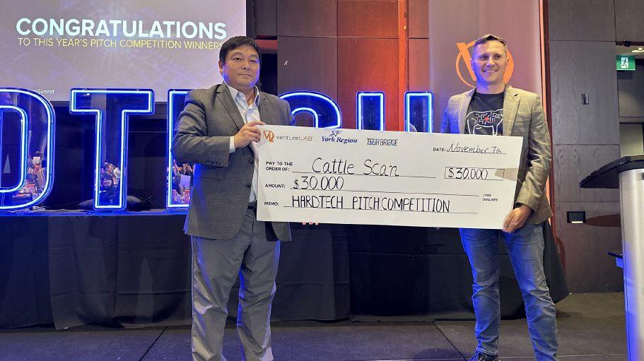
The second day of Hardtech featured the annual Pitch Competition, led by eight Canadian technology firms lined up to present their ground-breaking ideas in front of a panel of judges. Cattle Scan was crowned the first-place winner of the annual competition. Cattle Scan founder Denis Tokarev took home the prestigious Tech Bridge Award, securing a $30,000 non-dilutive cash prize for his cutting-edge livestock monitoring technology. Cattle Scan is a rumen bolus program that identifies cows with illness early, providing the opportunity for timely intervention and faster recovery. With 24/7 monitoring and personalized
alerts, our system assists in increasing milk production, reducing treatment costs, and optimizing labour on dairy farms.
GOOGLE QUANTUM AI UNVEILS ‘WILLOW’ QUANTUM CHIP
Google’s Quantum AI team unveiled Willow, a state-of-the-art quantum computing chip that has demonstrated the ability to not only exponentially correct errors, but also process certain computations faster than supercomputers could within known timescales in physics.
The announcement represents a significant milestone in the Quantum AI team’s journey to create a reliable quantum computer, that can “expand human knowledge for the benefit of all people,” according to Hartmut Neven, founder and lead of Google Quantum AI, described as a “new approach to computing, where people are building machines that use quantum mechanics — the fundamental language of the universe — to break through the limits of classical computing.”
Willow has state-of-the-art performance across a number of metrics, enabling two major achievements.
The first is that Willow can reduce errors exponentially as things scale up using more qubits. This cracks a key challenge in quantum error correction that the field has pursued for almost 30 years.
Second, Willow performed a standard benchmark computation in under five minutes that would take one of today’s fastest supercomputers 10 septillion (that is, 1025) years — a number that vastly exceeds the age of the Universe.
CMC MICROSYSTEMS SIGNS MOU WITH CSC
CMC Microsystems, Canada’s leading hardware accelerator and facilitator, has signed a Memorandum of Understanding (MOU) with Canada’s Semiconductor Council (CSC), a national semiconductor industry organization. Both groups have expressed a mutual commitment to working together on collaborative initiatives, leveraging both organizations’ strengths to enhance the country’s digital economy. Both parties believe that their combined efforts will bring benefits to the Canadian semiconductor ecosystem by fostering innovation and economic growth.
“We’re excited to formalize our relationship with Canada’s Semiconductor Council. By working together, we can ensure that Canadian researchers, start-ups and companies have access to the tools and expertise they need to innovate in a fast-moving global marketplace,” said Gordon Harling, president and CEO of CMC Microsystems. “This MOU is an important step in aligning our efforts to support the growth of Canada’s semiconductor ecosystem.”
Under the MOU, both groups will collaborate to strengthen Canada’s semiconductor ecosystem by promoting each other’s roles through various channels and holding regular discussions to explore new opportunities and address sector challenges. The two organizations will share insights and knowledge by participating in each
Cattle Scan founder Denis Tokarev (right) won the Hardtech Pitch Competition and a $30,000 prize.
other’s advisory boards, with Paul Slaby and Gordon Harling taking seats on the respective Boards of Directors.
FUNDING
CENGN LIVING LABS SUPPORTS STARTUPS
Backed by $45 million investment from the Federal Government’s Strategic Innovation Fund (SIF), the Canada’s Centre of Excellence in Next Generation Networks – or CENGN plans to develop eight Living Labs across Canada and support more than 100 Canadian startups and scaleups looking to prepare their innovative network technology products for market entry, commercial growth, and industry adoption.
CENGN Living Labs drive nationwide digital transformation for key
Canadian economic sectors. Through Living Labs, CENGN will provide the services, expertise and infrastructure required to test, validate and certify network technology solutions. This initiative will advance the competitiveness of Canadian industry while also supporting the development of new IP and the growth of our most innovative tech startups and scaleups.
TRANSPORTATION
GCXPO REVS UP NEXTGEN SMART MOBILITY
Area X.O, the R&D complex for nextgen smart mobility founded and operated by Invest Ottawa, recently held GCXpo (formerly TCXpo), the third smart mobility demonstration day showcasing innovators and companies from across Canada. The global tech hub hosted 80 live tech demonstrations and exhibits, while connecting participating founders and firms with potential customers, talent, investors and markets.
More than 1,600 stakeholders from
industry, government, academia and the investment community descended on the $51 million outdoor R&D complex to participate in the extensive demo day. The event creates a unique opportunity to experience the impact of cutting-edge homegrown technologies on diverse industry sectors, the world around us and our everyday lives.
“GCXpo demonstrates the growing leadership of innovators and companies from Canada’s Capital and across the country in the multi-billion-dollar global smart mobility market. It enables entrepreneurs and firms to showcase the impact of their homegrown solutions, and connect with prospective customers, investors and talent. This builds directly on our mission at Area X.O: to accelerate the commercialization of new technologies, and help get companies to market, customers and revenue faster, safely” said Sonya Shorey, president and CEO, Invest Ottawa.
Visit ept.ca for the latest new products, news and industry events.
Award-winning ultrasound system is a mixed-reality
UBC student invents ultrasound system for remote areas
BY MIKE STRAUS, WEST TECH CORRESPONDENT
Access to ultrasounds in remote areas is a significant challenge for the healthcare industry, both in Canada and worldwide. Hard to access communities often lack the local resources to perform ultrasounds, forcing patients to travel for days at a time to receive a simple scan. For David Black, a Ph.D. Student at the University of British Columbia in Vancouver, emerging technologies pose a potential solution to this challenge.
“We have very good healthcare in large cities, but it’s challenging to provide healthcare in small towns,” Black explains. “For ultrasounds, either a sonographer must travel around from community to community, or the patient has to travel to a major centre. In a lot of towns in northern Saskatchewan, for example, patients must spend several days traveling to get where they’re going, so a simple exam turns into three days of travel. It’s expensive, disruptive to work and bad for the environment.”
Black turned to technology in order to find a solution for these travel challenges and improve delivery of healthcare expertise for small communities.
Like a remote robot
It also led Black to research and develop a first-of-its-kind remote mixed-reality ultrasound system designed for use in small communities.
“The system is like a remote robotic ultrasound system, except that the robot is replaced by a human follower,” Black says. “The follower wears a mixed-reality headset, and they see through this headset a virtual ultrasound probe projected onto the patient. Their task is to take the real probe, align it with the virtual probe and follow it as it moves around. The virtual probe is controlled by an expert physician or sonographer.”
Black explains that the expert physician has a livestream of the ultrasound image, and is in verbal communication with the follower.The expert moves the input device as if they were doing the ultrasound themselves, which controls the virtual probe on the other end of
the system; the follower then follows the virtual probe with an actual ultrasound probe.
“The follower’s ultrasound probe has force-sensing capabilities and tracks its position and orientation visually from the headset,” Black notes. “We can feed the measured forces and any position-tracking error back to the expert, creating haptic feedback so the expert can feel in their hand as if they’re touching the patient.”
Black says that devising such a complex system wasn’t without its challenges. He notes that getting everything to run smoothly and reliably was tricky, as everything on the follower’s side runs on a single mixed-reality headset. Furthermore, once Black started testing the system in a community setting, he found that sonographers have a specific way of doing things that differs from what one might expect – they have a specific way of holding the input device, which means the input device had to be tailored to sonographers’ requirements.
“Another very tricky aspect, and probably the biggest technical challenge, is the communication delay in the teleoperation,” Black says. “Not only are we communicating over a long distance, which can obviously cause delays, but the follower also must react to what they see in the virtual probe and move to match it. There’s a reaction time element there, which causes a slight delay. Any kind of delay in teleoperation can cause instability, especially if we’re feeding back forces. So that’s the biggest technical challenge.”
Black notes that when developing his prototype, he used an off-the-shelf haptic device; this caused limitations with the system due to its limited workspace and force capacity. As a result, Black and his team are now developing a new haptic device. Developing a device for haptic feedback is a struggle because it must be lightweight enough to be moved around freely in space, but also strong enough to provide the right amount of resistance.
“The control aspect of things is tricky to stabilize, as well – it’s hard to transfer
haptic feedback with time delays.That’s the focus of my Ph.D. research; there are some very good approaches for doing this. One example is that instead of directly measuring the forces, we can create a 3D model of the patient using a depth camera, and then the haptic device can interact with the 3D model, which makes communication delays irrelevant.”
Black’s system differs from other teleoperation systems in a few key ways.There currently exist two primary approaches to telehealth ultrasounds. The first method is videoconferencing, which works well if the clinician already knows how to do an ultrasound, but is very imprecise and inefficient if not. The second approach is robotic teleoperation - effective, but impractical in small towns. His method bridges the gap between both techniques.
David Black, a Ph.D student at UBC is a Mitacs award recipient for his work on developing a remote robotic ultrasound system, which serves remote communities across Canada.
Black notes that his system has applications for any kind of ultrasound exam, including in trauma cases, obstetrics, and potentially physiotherapy. He says the system can even be used for teaching, providing hand-over-hand guidance on how to execute a task. The system also has potential applications outside of medicine, including industrial use cases for remote service maintenance and inspection.
Exciting to win award
Black says winning the MITACS Innovation Award for Outstanding Innovation has been important for him and his team:
“Initially it was just me and my Ph.D. supervisor working on this system. We got a partnership with Rogers and MITACS funding, which allowed us to hire a lot of undergraduate interns and graduate students to work on this technology with us.Winning the award is exciting; it shows that we’re on the right track and we’re doing something that matters.”
Black and his team are now in the process of performing clinical tests of the mixed-reality system.The team has conducted tests in small communities and hospitals in the Canadian North. Black is also iterating on the technology to make it possible to perform more advanced scans. Soon, the team will establish a startup company to deploy and commercialize the technology.
Mike Straus is EP&T’s West Coast correspondent. mike@brandgesture.ca
MIT-led research team aims to minimize enviro impact of electronics
BY ELIZABETH THOMSON, MIT MATERIALS RESEARCH LABORATORY
The microchips behind everything from smart phones to medical imaging can be traced to about 500 Megatonnes of CO2-eq lifetime emissions in 2021, and every year the world produces more than 50 million tons of electronic waste. Further, the huge data centers necessary for complex computations like on-demand video, are growing and will require 10 percent of the world’s electricity by 2030.
“This is neither scalable nor sustainable and cannot continue,” says Dr. Anuradha Murthy Agarwal, a principal research scientist at MIT’s Materials Research Laboratory.
To that end, Agarwal and colleagues have formed FUTUR-IC, a new Global Alliance for Sustainable Microchip Manufacturing, to perform research that will create novel high performance electronic-photonic integration technology while targeting circularity, with a STEM-trained green innovative workforce. FUTUR-IC is the result of funding from the National Science Foundation (NSF) Convergence Accelerator’s Track I: Sustainable Materials for Global Challenges. It is aimed at solving especially compelling societal or scientific challenges to sustainability using a multi-disciplinary approach that both captures the full product life cycle through the advancement of fundamental science and uses circular design to create environmental and economically sustainable materials and products.
FUTUR-IC, a reference to the future of integrated circuits, brings together stakeholders from industry, academia and government. The market for microelectronics in the next 10 years is predicted to be on the order of a trillion dollars, but most of the manufacturing supply chain for the industry resides only in limited geographical pockets around the world. FUTUR-IC aims to diversify and strengthen the supply chain for manufacturing and packaging of electronics and photonics.
The alliance already has 26 collaborators and is growing. Current external collaborators include the International Electronics Manufacturing Initiative (iNEMI), Tyndall National Institute, SEMI, Hewlett Packard Enterprise, Intel and the Rochester Institute of Technology.
FUTUR-IC is a new Global Alliance for Sustainable Microchip Manufacturing.
FUTUR-IC is organized into three dimensions - Technology, Ecology, and Workforce - that were defined with the help of feedback from some 140 stakeholders during Phase One of this NSF Convergence Accelerator program.
“We have become accustomed to the benefits forged by the exponential growth of microelectronic technology performance and market size,” said MIT’s Lionel Kimerling, who is also co-director of the MIT Microphotonics Center. “The ecological impact of this growth in terms of materials use, energy consumption and end-of-life disposal has begun to push back against this progress. We believe that concurrently engineered solutions for these dimensions will build a common learning curve to power the next 40 years of progress in the semiconductor industry.”
Reduce, ecological footprint
He continued, “Dr. Agarwal has uniquely created the vision and pathway to maintain technology growth using electronic-photonic integration, and reduce ecological footprint with lower energy consumption, use of legacy nodes for photonics, and easier access to repair and disassembly due to longer interconnects enabling spatially separable components. Her energy, collegiality, and leading-edge contributions to the science of chipmaking have combined to build the research teams that underlie the FUTUR-IC Global Alliance for Sustainable Microchip Manufacturing. The Alliance is fortunate to have her leadership and her vision to guide Technology, Ecology and Workforce into the next stage for the industry.”
FUTUR-IC is investigating innovation in sustainable electronic-photonic
packaging. Additionally, in conjunction with partners, FUTUR-IC will develop novel materials and designs that enable one to reduce, reuse, recycle, repair and upgrade microchip-containing systems.
The current microchip scaling trend requires judicious use of mixed technology chiplets for higher speed and increased functionality within a standard electronic-photonic package platform. FUTUR-IC is enabling this foundational platform to achieve a package I/O target of 1.6 Pb/s data rates using chip-to-chip evanescence and micro-reflection within photonic interconnects. This form of electronic-photonic integration enables modularity for easier disassembly and helps meet ecology constraints of affordable and accessible repair of microchips in systems, decreasing energy consumption and cutting waste and greenhouse gas emissions associated with electronics.
Universal quantitiative tool
“We expect the integration of electronics and photonics to revolutionize microchip manufacturing, enhancing efficiency, reducing energy consumption, and paving the way for unprecedented advances in computing speed and data-processing capabilities,” said technology co-lead Serna reiterates these benefits of photonics.
An example of work underway in the ecology dimension is the development of a universal quantitative tool across the semiconductor supply chain to help industries assess the environmental impact of their design and operational decisions.
“The microchip industry must have transparent and open Life Cycle Assessment (LCA) models and data, which are being FUTUR-IC will also detect and minimize the use of toxic forever chemicals, per- and polyfluoroalkyl substances (PFAS) in the microchip manufacturing ecosystem,” Serna continued. “Enabling the detection, capture and remediation of PFAS, as well as the development of PFAS-free polymers for microchip processing and electronic-photonic packaging within the semiconductor industry, will be an important contribution to environmental sustainability in microchips as well as to other industries needing alternatives.
Promise and peril
Chip supply shifts gears for Canada’s transforming automotive sector
BY CANADA’S SEMICONDUCTOR COUNCIL
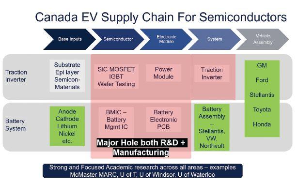
The rapid adoption of electric vehicles (EVs) and hybrids (including PHEV and HEV) is reshaping the global automotive industry. At the heart of this transformation lies the increasing reliance on semiconductors, specifically power electronics, with estimates suggesting that up to $2000 of an EV’s bill of materials will be semiconductors, and over 1,500 semiconductor components are found in a typical vehicle today. However, a recent report by Canada’s Semiconductor Council (CSC) Automotive Microchips Working Group reveals a significant gap in Canada’s automotive semiconductor supply chain for EV’s, posing risks to Canada’s investments and ambitions in this sector. This is of particular importance given the large amount of funding and incentives (totaling near $40B) recently committed by
our government to the rapidly transforming Canadian automotive sector.
While Canada has made strides in the final stages of the EV supply chain, particularly in vehicle assembly and EV batteries, these investments rely on a supply chain that is almost entirely offshore. The report findings highlight that there is minimal Canadian content across the EV supply chain, with Canada’s primary focus on servicing internal combustion engines (ICE), or non-electronic components such as plastics and mechanical products.
With the bulk of the EV supply chain concentrated in regions like Asia and Europe, this creates a dependence of Canadian EV manufacturers on foreign suppliers. Such a reliance not only increases supply chain vulnerability (as illustrated by the supply chain disruptions and geopolitical
tensions during the COVID-19 pandemic), but also limits Canada’s ability to maximize on the economic opportunities driven by the EV market expansion.
Challenges: Perspective from Semi Ecosystem
Lack of domestic companies in automotive semiconductors: Canada has limited presence in the automotive semiconductor sector, including manufacturing, traction inverter design in the US supply, and design, packaging, and electronics assembly.
Need foreign suppliers?
The EV supply chain heavily relies on foreign suppliers, with mainly the final stages of battery and EV assembly based domestically. This dependence extends to semiconductor components as well as the power modules and systems used in EV traction inverters, DC-DC converters, onboard chargers, and battery management systems.
Insufficient research
Although Canada excels in academic research related to semiconductors and electric motors for electric vehicles, there is a need for better connection to the Canadian automotive industry and manufacturing, limiting commercialization efforts.
Global competition and vertical integration
Regions like China are becoming vertically integrated, capable of producing nearly everything needed for EVs, including semiconductors, power electronics, batteries, and systems.
Opportunities: Building on Canadian strengths
Despite these challenges, the report highlights several areas where Canada could establish a leadership role.
Strong academic footprint in automotive power Canada has leading academic institutions conducting research in EV-related areas like electric
Paul Slaby, managing director for Canada’s Semiconductor Council, is inviting electronics industry stakeholders to join the group’s consortium.
motors, power electronics, and new materials. Examples include the McMaster Automotive Resource Center (MARC), University of Toronto, University of Windsor’s Charge Lab, and École de technologie supérieure (ÉTS).
Adjacent markets & ecosystems
Canada’s established strengths in adjacent markets provide a solid foundation for growth in the EV supply chain. These include the Bromont semiconductor manufacturing ecosystem, expertise in hydrogen fuel cell technology led by Ballard Power, and the large digital semiconductor design talent ecosystem in the Greater Toronto Area (GTA).
Legacy ecosystem
Ontario’s automotive assembly operations and existing ICE supply chains offer strong foundations for building a robust EV supply chain. Although specializing in legacy technologies, the value of the relationships within the supply chain could be leveraged.
Building a resilient, self-sufficient supply chain
Develop a power electronics R&D consortium
Focus on bridging the gap between academic research and industrial application by funding commercialization projects and fostering partnerships between academia and industry. Actionable recommendations include establishing an Automotive and New Mobility Power Electronics Consortium, and targeted funding for R&D commercialization.
Create a long-term automotive semiconductor manufacturing strategy
Develop a cohesive strategy that integrates semiconductor production with key value-added local manufacturing to reduce Canada’s reliance on imports. While no single
country can independently supply all the semiconductor components required for future EVs, partnering with other nations and leveraging their respective strengths can allow Canada to create a complete and well-defined EV supply chain.
Canada has a choice to make–continue to rely on offshore supply chains, or seize the opportunity to build a resilient, self-sufficient supply chain. CSC’s Automotive Microchips Working Group report aims to serve as a foundation for creating Canada’s Automotive Semiconductor Innovation Roadmap, by defining specific areas where government investment, policy support, and collaboration can propel Canada to rise to the occasion.
It’s proposed that the consortium will be housed in a university R&D hub, such as the McMaster Automotive Resource Centre (MARC) at McMaster Innovation Park. This location offers state-ofthe-art infrastructure, prototyping and testing facilities, and manufacturing expertise, as well as established connections with major OEMs and Tier 1 suppliers.
This article is the result of collaborative efforts led by leaders within the Canada’s Semiconductor Council including Kirk Ouellette, VP of global strategy, STMicro; Paul Slaby, managing director, Canada’s Semiconductor Council; Brett McQueen, director of innovation, North America, Linamar Corp.; Benoit Rousseau, product line head, Infineon Technologies; Ali Emadi, professor and Canada research chair in transportation electrification and smart mobility, McMaster University, and the contributions of 27 participants from 13 organizations and individual consultants.
For access to the full report, visit: www.canadassemiconductorcouncil. com/csc-automotive-microchipsreport-landing-page
A call to industry: Join the consortium
As Canada aims to strengthen its position in the global semiconductor value chain, the Canada’s Semiconductor Council (CSC) has unveiled an ambitious initiative: the Automotive and New Mobility Power Electronic Consortium. This proposal invites stakeholders from across the Canadian electronics industry to collaborate in shaping the future of power electronics for next-gen solutions in these sectors.
In this Q&A, we ask Paul Slaby, managing director for Canada’s Semiconductor Council to outline the vision and objectives of the consortium, while encouraging participation in Canada’s chip ecosystem.
Q. What are the primary goals of the Consortium?
The group aims to foster collaboration across the automotive and semiconductor industries to facilitate a strategic transition towards EVs. The consortium’s goals align with Canada’s broader semiconductor strategy by promoting strategic investments, R&D and commercialization, while integrating semiconductor manufacturing into local industries.
Q. Managing collaboration between stakeholders & academia
The consortium will facilitate collaboration between industry and academia through a structured partnership framework. Industry will lead governance, ensuring research aligns with automotive needs. Industry stakeholders will play a central role in defining the consortium’s agenda, providing financial support, and guiding its direction to maximize the relevance and impact of research outcomes. A core research team of academic experts will contribute specialized knowledge, with industry partners leading research topics to ensure practical solutions. The consortium will be housed at a major university R&D hub with a strong focus on automotive electrification, such as the McMaster Automotive Resource Centre (MARC) at McMaster Innovation Park.
Q. How do you ensure the group is responsive to market demands?
The consortium’s governance model integrates industry leadership and strategic oversight. A Board of Directors, composed of key industry stakeholders, will oversee R&D, focusing on critical EV technologies like power electronics, battery systems, and advanced semiconductor components for the next generation of electric and autonomous vehicles. A Steering Committee of political and economic leaders will provide insights into public policy, funding strategies, and regional economic priorities, to align efforts with national goals. Specialized committees will address specific topics in EV component design, manufacturing and supply.
Q. What role will academic researchers play as core members?
Academic researchers will contribute expertise and innovative solutions to advance research, development and commercialization in automotive power electronics, packaging and systems. The leadership structure will enable a collaborative partnership between academia and industry, where academic researchers lead specialized research topics while working closely with industry leaders. Industry stakeholders will provide strategic guidance, ensuring that research efforts are aligned with market demands, practical applications and commercialization pathways.
Q. What specific components will the group focus on?
The consortium will focus on developing and manufacturing key power electronics components and software for EVs, including: control electronics, circuit components, protection devices, connectors & busbars, semiconductor gate drivers, inductors & capacitors, sensors, thermal management solutions, and packaging & mechanical parts. This is essential for the mass production & performance of EVs.
Interested parties can contact CSC to learn about its initiatives, working group and access published reports, or join as a member, at www.canadassemiconductorcouncil.com
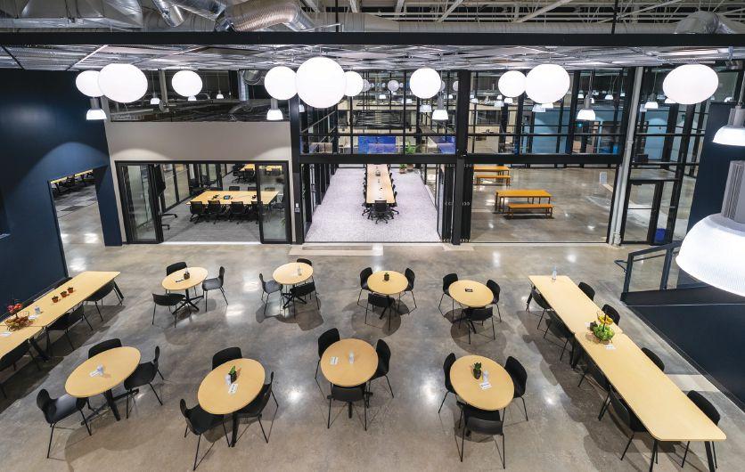
KW tech hub expands into automotive, mobility sector
OVIN joins Catalyst Commons - Canada’s largest privately held co-working space
Catalyst Commons, Kitchener’s fastest-growing co-working tech space, unveiled its recent expansion of the facility. At more than 125,000 square feet, the addition solidifies it as Canada’s largest privately held co-working space and further positions Catalyst as Waterloo Region’s leading hub for entrepreneurial innovation.
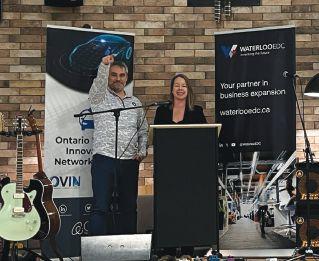
In addition, Catalyst also announced its role as the first operational site under the Ontario Vehicle Innovation Network (OVIN) Incubators initiative. Announced by Ontario Premier Doug Ford earlier this year, this initiative will serve as a catalyst for Ontario’s automotive and mobility sector, accelerating the creation and growth of new Ontario-based companies and connecting them with the global market.
“Catalyst has truly become the home base for builders in Waterloo Region,” says Amber French, co-founder of Catalyst Commons.
“It’s a place where you can fi nd startups working alongside some of Canada’s top scale-ups, multinationals, investors, community not-forpro fi ts, post-secondary institutions and supporting businesses. Everything you need to start and scale a business can be found under one big roof.”
Bridging the gap
Founded in 2020 by serial entrepreneurs Kurtis McBride, Amber French and Angela Watkins, Catalyst Commons is an industry-driven centre for businesses of all sizes, promoting collaboration, growth and innovation. Since its inception, Catalyst has attracted over
Catalyst Commons is Canada’s largest privately held co-working space, spanning 125,000 square feet within Catalyst 137, a large IoT-focused innovation hub.
150 companies, creating a vibrant ecosystem for businesses to thrive. Among the latest additions to the Catalyst community are industry giants such as Bloomberg, IMAX, Conga, Miovision and IPON, McCallum Santher, Skillswave, ThinkLP, Bridgit, Cabinovo and DialPad. As part of this collaboration with Mercedes-Benz as the first partner, the OVIN Incubators are designed to bridge the gap between applied research and the commercialization of intellectual property, connecting industry leaders, startups, scale-ups and post-secondary institutions. As part of this collaboration, the Kitchener-Waterloo site at Catalyst. Commons will host space for entrepreneurs and startups, connecting regional activities in this area focused on building the next generation of Ontario-based automotive
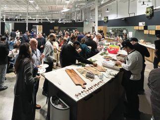
Above-left: Catalyst Commons unveiled the facility’s expansion of more than 125,000 square feet. The addition solidifies it as Canada’s largest privately held co-working space and further positions Catalyst as Waterloo Region’s leading hub for entrepreneurial innovation. Top-right: Invited guests gather at the opening event function hosted at Catalyst Commons in Kitchener ON; Bottom-right: Kurtis McBride and Amber French, co-founders of Catalyst Commons celebrate the opening of the expanded hub.
Photos Source: Catalyst Commons
and mobility ventures and strengthening the province’s automotive supply chain.
“The future of Ontario’s automotive and mobility sector requires a robust foundation to nurture the next generation of innovators, entrepreneurs and homegrown companies,” said Raed Kadri, Head of OVIN. “As the first incubator program of its kind in Ontario and across Canada, the OVIN Incubators will leverage Kitchener-Waterloo’s unique regional expertise to build a launchpad for new Ontario-based automotive and mobility ventures. Together, we are strengthening Ontario’s position as a global leader and building the supply chain of the future, driving prosperity for generations to come.”
“This partnership with OVIN marks just the beginning of an exciting journey,” adds French. “We’re committed to building a sustainable, entrepreneur-led innovation model, and we’re exploring additional collaborations to enhance our incredible community. 2025 is going to be an extraordinary year for Catalyst Commons.”
Bringing together start-ups
“Catalyst Commons’ expansion and its role as the first operational site under the OVIN Incubators initiative represents a significant milestone for Ontario’s innovation ecosystem,” said Claudia Krywiak, president and CEO of the Ontario Centre of Innovation. “By bringing together startups, scale-ups, industry leaders, and post-secondary institutions, this partnership demonstrates the power of collaboration to drive transformative advancements in automotive and mobility technologies. With this unique co-working space and the support of global leaders, Catalyst Commons is not only fostering innovation but also solidifying Ontario’s reputation as a global leader in the future of transportation.”
The following is a list of new companies joining the Catalyst Commons: Bloomberg; Bridgit; Cabinovo; Conga; DialPad; Ducimus; Capital H2O;
Opened in late 2020, Catalyst Commons is Canada’s largest privately held co-working space, spanning 125,000 square feet within Catalyst 137, a large IoT-focused innovation hub. Catalyst Commons operates as a
distinct co-working space within the larger Catalyst 137 facility. Catalyst Commons offers services tailored to startups, growing companies, and teams of various sizes. It provides private offices, shared workspaces, and amenities designed to foster collaboration and innovation. Both entities are part of the ecosystem at 137 Glasgow Street but cater to slightly different needs within the tech and entrepreneurial community
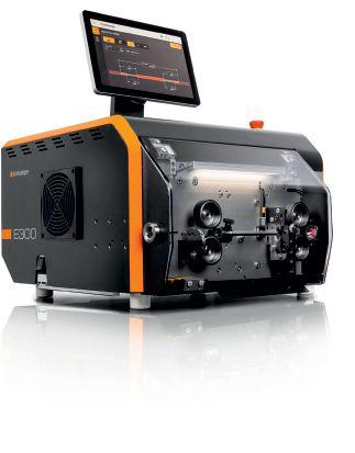
To Be Reliable
Cut & Strip Family E300
schleuniger.com 905-827-1166
Transform Your Cable Processing
Experience unparalleled reliability and ease of use with the high-performance E300. Designed to handle a variety of wires, cables, and insulation materials with precision, the E300 ensures top-quality results. Seamlessly integrate the E300 with a wide range of peripherals to create an automatic processing line, boosting efficiency and performance.
Processes conductor cross sections from 0.05 to 10 mm² (36 to 8 AWG)
Intuitive interface simplifies job creation and setup
Quick software-assisted troubleshooting
Programmable clamping axis for greater accuracy
Two-in-one quick-change feeding unit, including a short piece kit for processing short cables
Wire Solutions for a Connected World
Navigating the complexities of semiconductor product lifecycles
Q&A with Rochester Electronics demystifies steps required to safeguard against component obsolesce
The semiconductor industry is the backbone of modern electronics, but managing product lifecycles in this fast-evolving sector is no small feat. From ensuring long-term availability to addressing supply chain disruptions, the challenges are as diverse as they are critical.
In this Q&A, we sit down with Rochester Electronics, a global leader in semiconductor lifecycle solutions, to explore their insights on navigating the complexities and supporting customers through every phase of the product lifecycle.
What are the biggest challenges in managing lifecycles?
As silicon fabrication technology advances, older processes are phased out. Due to limited equipment and expertise, producing legacy components is challenging.
The shift to advanced silicon fabrication reduces the availability of raw materials and equipment, causing suppliers to phase out older materials and machinery, which creates sourcing challenges for legacy systems and raises obsolescence risks.
These changes accelerate component obsolescence. Thus, manufacturers seeking efficiency and reliability often adopt new processes that are incompatible with older components like PLCC and PQFP.
Innovations can render legacy components obsolete, as new materials provide improved performance, such as higher thermal stability and
enhanced conductivity. This shift may result in the discontinuation of older materials, complicating production and support for legacy components.
Component manufacturers often discontinue unprofitable parts as demand shifts to newer technologies, focusing on in-demand parts with better profit margins. Producing small quantities of obsolete items can be cost-prohibitive.
Obsolete components can disrupt supply chains, affecting production schedules and complicating sourcing authentic, quality replacements.
Addressing component obsolescence can lead to added costs for redesign, re-certification, sourcing new components, and retraining, straining budgets and affecting timelines.
How has the supply chain evolved, and how has it impacted obsolescence?
The COVID-19 pandemic revealed weaknesses in the semiconductor supply chains, leading to panic and overordering as sectors sought critical components amidst supply constraints. Challenges intensified from wafer fabrication to testing, with wafer procurement becoming especially difficult and lead times increasing over fourfold due to factory worker shortages.
Geopolitical events have severely threatened industry supply chains, constraining critical materials such as aluminum, nickel, palladium, titanium, and automotive wire harnesses.
The semiconductor industry faces
challenges with rapid component obsolescence and Pb-free assembly, leading to OSAT consolidation. Current EOL and last-time-buy issues arise from a focus on new products after a market boom, while CHIPS Act investments emphasize leading-edge technologies over legacy products.
The market has shifted from oversold to undersold, with a prolonged downturn in 2024.
Why is semiconductor lifecycle management critical for the aerospace, automotive, and healthcare industries?
The COVID-19 pandemic revealed weaknesses in the semiconductor supply chains, leading to panic and overordering as sectors sought critical parts amidst supply constraints.
Due to their reliability, legacy systems in industries like aerospace, automotive, and healthcare must be preserved. Replacing them with untested systems can pose risks, lead to regulatory issues, and cause costly failures, including high expenses for new equipment and training.
Component obsolescence challenges designers by threatening legacy systems with outdated parts. They must balance finding obsolete components and integrating modern technologies.
How can OEMs / designers mitigate risks?
Proactively addressing component obsolescence is crucial for smooth operations. Tools like Z2Data and Accuris can track component lifecycles and end-of-life dates, helping
organizations forecast and manage obsolescence-related costs effectively.
Predicting EOL is unreliable despite tracking component lifecycles. Unforeseen events like supplier consolidation or natural disasters can disrupt forecasts. Over 30% of discontinuations occur without prior warning, going directly from active to EOL.
Component obsolescence and requests for ‘Last-Time-Buys’ require customers to predict future equipment sales, but these forecasts can be unreliable due to unforeseen market changes.
Sharing the Bill of Materials (BOM) with component suppliers helps customers identify project risks and proactively plan to mitigate obsolescence.
How can OEMs balance the need for innovation with the challenge of supporting legacy systems?
Successful long-term system companies balance their designs by anticipating semiconductor changes. They maintain communication with aftermarket manufacturers and providers to prepare for shifts before LTB notices.
What role do third-party suppliers play in ensuring the availability?
Product lifecycles can outlast the availability of semiconductor components, making lifecycle status essential in the new product introduction (NPI) process. If critical components reach end-of-life (EOL) before the product matures, a reliable long-term supply chain for semiconductor lifecycle solutions is necessary. When the original component manufacturer
(OCM) discontinues a product, they often offer a ‘Last-Time Buy.’ However, customers might struggle with the cost, volume requirements, or storage for future needs.
Unprepared companies face risks of counterfeits and quality issues. Authorized distribution players can provide a dependable source with storage solutions. Partnering with a licensed semiconductor maker can reduce the risks of component EOL by enabling the production of discontinued devices.
What are the key elements of a successful obsolescence strategy?
It begins at the design and product definition phases. We’ve all heard stories of products launched with obsolete components, especially affecting customers with long development cycles.
Choosing the right component technology and supplier is crucial for long-term availability, and the lowest-cost options may not be the best choice.
Some key points to consider include: What is the component’s lifecycle status during the application’s lifetime? Are the design’s key components fully documented? Can true design files be archived for rebuilding if needed? And, does the design include proprietary intellectual property?
What are the key considerations to understanding the total cost of obsolescence?
It’s important to identify whether or not the product project plan needs a refresh or redesign funding?You must also consider what impact component obsolescence might have on after-sales service, and will a shortened
lifecycle affect customers and end-users.
How do you plan for obsolescence and resource management?
If your equipment has extended qualification, production, or in-service lives, you will face component obsolescence. Organizations should devote skilled, multi-disciplinary workers to obsolescence management. Preventive planning can reduce or eliminate costs and risks.
Identifying PDNs
It is imperative to identify Product Discontinuation Notices (PDNs) that may affect your business. Proactively monitoring component lifecycles is essential for anticipating issues. Reliable commercial tools track lifecycle stages, lead times, and specification changes and provide alerts for PDNs. Some key questions to ask yourself include: Will your sub-tier suppliers share their BOMs; and do they have adequate obsolescence management processes?
While many component electronics manufacturers offer proactive component lifecycle management as a service, others are entirely reactive.
Last Time Buy (LTB) - Forecasting
Forecasting is inexact, making it hard to predict product needs and market disruptions. Underestimating can lead to premature terminations while overestimating results in excess costs. Future redesigns should account for design, requalification, and engineering resource costs.
100% Authorized suppliers
Many think only grey market sources exist for discontinued components, however, authorized after-market suppliers serve as safe choice.
Counterfeit and poor-quality components from unauthorized sources harm production yields and Mean Time Between Failure Rates (MTBR). Inferior testing by unauthorized third parties leads to a false sense of confidence in authenticity. Unauthorized component risks include: Poor handling can cause ESD damage and device failure.
• Inadequate storage may lead to corrosion and moisture issues: lead corrosion, failed solderability, moisture ingress, and device failure.
• Fake documentation that mimics the original specification or misrepresents performed tests.
• Recovered, re-marked, or repackaged components.
PRODUCTION EQUIPMENT
Photo Source: Getty/ gorodenkoff
Waterloo’s MSAM Lab emerges as global additive manufacturing powerhouse
Once a tiny lab, facility increases capacity for research, training and partnerships to meet growing demands in the field of advanced manufacturing
BY DARREN MCALMONT, UNIVERSITY OF WATERLOO
From its humble beginnings in a 150-square-foot, windowless room in 2004, the Multi-Scale Additive Manufacturing (MSAM) Lab at the University of Waterloo has grown into Canada’s largest academic research lab for metal additive manufacturing. With over $25 million in infrastructure, it now stands as one of the most advanced university-based metal AM facilities in the world.
The expansion of the lab enables both industry and students to access top-tier expertise and equipment, facilitating the comprehensive development, iteration and validation of additively manufactured products from raw materials to finished goods by applying advanced scientific discoveries to industrial contexts.
The research conducted by MSAM is shaping the future by working with industry, institutions and communities. These partnerships infuse research solutions into sectors critical for economic growth and innovation by fostering collaborations with industry leaders and promoting technology transfer.
“The team at MSAM has strategically aimed for innovation while developing the next generation of metal AM technologies — another way of saying 3D printed products.” says Dr. Ehsan Toyserkani, a Waterloo engineering professor and founder of the MSAM Lab. “We excel in novel material adoption and development, as well as creating innovative quality assurance algorithms and software solutions to enhance the resilience and sustainability of part production.”
Reflecting on the success and growth of the lab over the years, Toyserkani shares that its early success began in 2005 through a collaboration with Mount Sinai Hospital at the University of Toronto and biomedical researchers from other universities. Across the span of six years, the collaboration resulted in a patented 3D printing technology for creating anatomically shaped implants from a
novel biodegradable material called calcium polyphosphate.
“The MSAM Lab is developing technologies for the future,” says Dr. Mihaela Vlasea, Waterloo engineering professor and co-director of the MSAM Lab. “It significantly transforms both large and small-scale advanced manufacturing while accelerating sustainability. The lab enhances clean technology and responsible production by adopting economically- and environmentally sustainable materials by minimizing waste through precise material deposition, which reduces excess consumption and energy use.”
Lab serves as central hub
With a new facility spanning approximately 15,000 square feet, the lab serves as a central hub for research teams and houses cutting-edge metal additive manufacturing printers and characterization devices. This expansion was partly funded by the approval of large equipment grants from the Federal Economic Development Agency for Southern Ontario, Canada Foundation for Innovation and the National Research Council. The larger, safer facility supports industry and fosters economic development by increasing capacity for research and development (R&D), validation, and technology transfers to meet growing demands in the AM field.
The facility has also attracted top research talent, strengthening Waterloo’s position on the global map for scholarly discoveries in additive manufacturing.
“By consolidating all critical devices under one roof, we streamline operations, encourage collaboration and prioritize safety,”Toyserkani shares. “The space also provides unique facilities for undergraduate and graduate students as well as a gateway for industry to explore AM technologies and collaborate together to mitigate R&D risks.”
More importantly, MSAM’s research significantly enhances Canada’s research capabilities, increases societal impact, and addresses complex global challenges through innovative solutions. This is evident from MSAM’s leadership role in a national strategic network called “Holistic Innovation in Additive Manufacturing” (HI-AM), which includes seven Tier 1 universities from coast-to-coast.
Businesses can leverage MSAM for a variety of additive manufacturing needs, including advanced prototyping and customization of products, including those not yet commercially available. The lab also provides training programs to cultivate a sustainable workforce of skilled advanced manufacturing professionals.
As Waterloo embraces additive manufacturing’s potential for innovative R&D through MSAM, it stands at the forefront of advancing custom-product development, providing intelligent quality assurance platforms and shaping the future of AM.
MSAM’s growth has created numerous employment opportunities and new R&D programs, attracting investments from the aerospace, automotive, energy and nuclear, natural resources and mining, and biomedical industries.
“Some post-graduate students who worked at MSAM as research associates and project managers have gone on to establish start-ups like Brickeye, OptiFab, and Formions,”Vlasea says. “Others have become professors at top universities in Canada and the United States or joined leading AM companies.”
Looking ahead, MSAM’s mandate is focused on not only continuing the track record of scholarly excellence and R&D industry engagement, but also on developing new industry training programs, training more students, helping industry to adopt and scale AM and producing more patents and intellectual properties.
Explore millions of components for your next design
Although a trek to this active volcanic island is strictly prohibited, you have unlimited access to millions of electronic components, from well over a thousand leading brands engineers know and trust. Discover the hottest components for design.
mouser.com
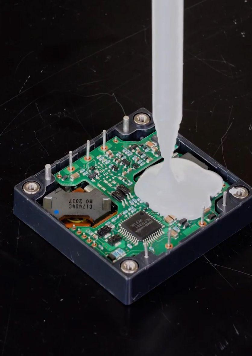
Thermal management materials cool AI ecosystem designs
How advanced silicones handle heat, stress and more
BY HONGQING CHEN, GLOBAL SEGMENT LEADER, DOW CONSUMER & ELECTRONICS
AI technology development for consumer electronics, telecommunications infrastructure and cloud and data centres call for a greater density of high-power components into smaller spaces. As power requirements and energy consumption rise, the amount of heat generated also increases. Unless this heat is dissipated, electronics devices are at risk. The consequences can range from diminished or degraded performance to device or system failure.
Advanced silicones for thermal management are well-suited for solving AI ecosystem challenges. These heat management materials can resist higher temperatures while providing longer-lasting heat resistance without a significant loss in properties. With their low modulus, they also can relieve some of the stress that results when different electronics materials, such as metals and plastics, expand and contract at varying rates because of their different coefficients of thermal expansion (CTEs).
Thermal management material types
There are many categories of thermal management materials, but silicone thermal gels and silicone thermal greases are especially effective at moving heat away from electronic components such as central processing units (CPUs) and toward cooling components such as heat sinks. Both types of products have a relatively high thermal conductivity.
Silicone thermal gels are applied to the surfaces of electronic components and compressed to a very low thickness, which improves heat transfer. They will not dry out for a long time and can be compressed indefinitely between a heat source and a heat sink. Silicone thermal greases are also used to improve the transfer
Advanced silicones for thermal management are well-suited for solving AI ecosystem challenges.
Photo Source: DOW Inc.
of heat between two surfaces; however, unlike gels, greases do not require curing but provides thinner bond line thickness (BLT).
Both types of products provide advantages over thermal pads, which are solid materials that can leave small gaps where air can enter. These micro-gaps are a problem because the thermal conductivity of air is around 0.026 W/mk. By contrast, silicone thermal gels and silicone thermal greases have significantly higher thermal conductivities.
Thermal gels
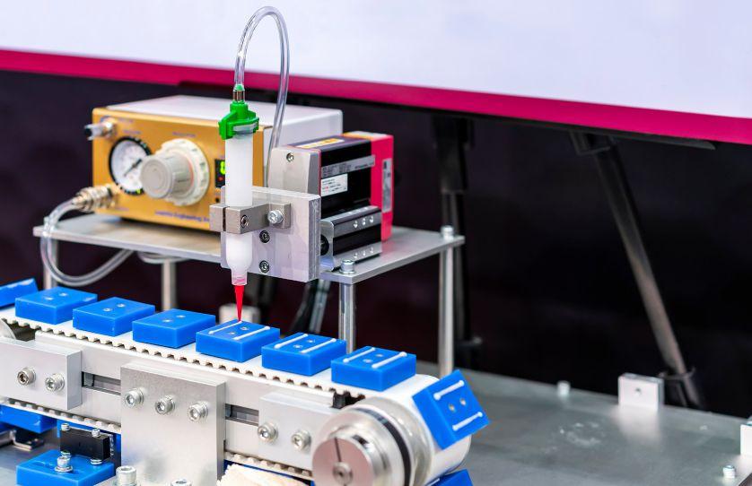
Silicone thermal gels are used in 5G electronics that demand greater power-chip efficiency. They are available in one-part formulations or two-part formulations. Silicone thermal gels are an excellent choice for high-volume assembly because they can be applied readily with automated dispensing, stenciling, or screen-printing equipment for greater production efficiency. These reworkable materials help reduce waste and can be peeled off easily and completely without residues.
Some silicone thermal gels are supplied as non-flowable pastes that resist slumping, which is the tendency to spread excessively and overflow the edges of a chip or other heat-generating component. Slumping can also leave too little paste behind, creating air gaps or air bubbles. For reduced stress concentrations, these soft paste-like gels can be pressed down to very thin bond lines measured in microns (µm). Room-temperature curing promotes energy efficiency but heat from ovens can be applied for accelerated curing.
Among their advantages, silicone thermal gels resist shock, moisture, humidity and a wide range of temperatures. That is important with devices like smartphones and laptop, which are occasionally dropped and often used in outdoor environments.
Additional applications for thermal gel include optical transceivers, which are small but powerful devices for sending and receiving data at the significantly faster transmission speeds; and base stations, which manage 5G’s high frequencies and bandwidths.
With optical transceivers, silicone thermal gels move heat from the device’s core components to a metal
shelter that serves as a heat sink. In base stations, these TIMs can be used with power amplifiers and power-supply rectifier modules, and between baseband unit (BBU) chips and heat sinks. The signal conversion, processing and transmission that these BBU chips perform require significantly more power than in a 4G base station, and this increased power consumption increases heat generation which can be dissipated by silicone thermal gels.
Silicone grease
Silicone thermal greases are used in higher power density applications that require superior heat dissipation including bare die architectures for computing and communications. Examples include high-performance CPUs and lidless graphics processing units (GPUs) for datacenter server, field programmable gate arrays (FPGAs) and application-specific integrated circuit chips (ASICs) for industrial computing.
Traditional thermal greases cannot match advanced silicone products in terms of resistance to pump-out, which is the loss of grease from the interface. In electronics, pump-out occurs when a device is subject to rapid temperature changes. The resulting expansion and contraction of the interface surfaces produces a pumping effect that can cause traditional thermal grease to be squeezed or pumped out from the interface, which reduces thermal transfer.
In addition to resisting pump-out, silicone thermal greases have a low thermal resistance for more efficient heat transfer compared to traditional thermal greases. They are also reworkable. These thixotropic products flow more readily when agitated but then
5G
electronics that demand greater power-chip efficiency use silicone thermal gels.
recover their original viscosity in a fixed time after shear loads have been removed. Once applied, silicone thermal greases can also achieve a low bond thickness measured in microns (µm).
Silicone thermal greases are supplied as one-part products and available in formulations with no added solvents. These products provide more consistent properties over a grease’s shelf life, even after a container is opened. Solvent-free products can also support regulatory compliance and environmental sustainability initiatives. Among their advantages, silicone thermal greases have a low hardness value that minimizes the generation of internal stresses.
Thermal solutions
As AI technology puts more high-power components into smaller spaces, designers need to address heat and stress. Yet, energy efficiency, environmental sustainability, and support for automated production are also key concerns. Increasingly, forward-looking companies want to develop AI-embedded technologies while also improving operations and reducing their carbon footprint.
For complete thermal management solutions, electronics designers need suppliers with proven products and a broad portfolio of materials. By taking a collaborative approach to material selection, the right supplier can recommend the best thermal gel or thermal grease for an application, while helping designers avoid problems such as slumping and pump-out.
Dow is a world leading materials science company, serving customers in the electronic design sector. www.dow.com/en-us
You would be hard pressed to find another cord maker who changes 100 lb. die molds up to 40 times a week just to meet our country-specific cord set orders, including IEC 60320 cords and components. More common is for cord makers across the globe to run one mold for weeks at a time to produce hundreds of thousands of the same cord—without all our quality checks! Interpower testing exceeds the testing requirements set by household agencies such as UL, CSA, and VDE. We test our cords throughout every phase of the manufacturing process. And test them again before shipping!
“We test more than the standards require for our own benefit. We do so because it lends better reliability to our design.”
Ron Barnett: Interpower Product Development Manager
Interpower cords come ready to use right out of the box to safely connect to your mains power. No reconfiguration is needed.
You will also find a few robots with ridiculous names working alongside dedicated humans who actually make our cords and components. You will find a can-do culture, superior raw materials, and a quality plan ensuring your built-to-last power cords work every time. Want your cords hanked, coiled, tied, bagged or boxed? Need them with special barcodes or labels? Done. Interpower offers other value-added options such as lengths, colors, and cord clips.
At Interpower, what we say about our cord sets and components is actually what we make. In a world with overburdened electrical grids, you’re going to need reliable cords whether plugging into a standard country-specific wall socket, an accessory power strip or power distribution unit, or a generator.
• 1-week U.S. lead-times
• In-stock cords ship the same day
• Quick-change molding process
• No minimum orders
Scan the QR Code to Learn More
Mitigating risks against supply chain disruptions
BY CHANELLE DUPRE AND KARTIK IYER, AVNAN
Supply chain challenges pose significant risks for businesses that rely on a global network of manufacturing and product design partners. Electronic Engineers at OEM companies, at one time or another, may have faced these challenges during the new product introduction (NPI)[PC1] process. External factors such as geopolitical conflicts, labour strikes and natural disasters or accidents, can all adversely affect business operations and [PC2]product development, while internal factors, including inefficient inventory management, complex multi-vendor relationships and weak supplier relationships, can exacerbate these challenges.
Both internal and external factors can lead to cost fluctuations, unpredictable lead times and quality issues, compromising a project’s viability and its competitive market advantage.
While many industries have increased their resilience in managing supply chain disruptions since the pandemic, the electronics sector remains particularly vulnerable due to its reliance on offshore markets. Though some of these challenges may be beyond the engineering team’s control, strategic planning can mitigate risks and help to navigate through supply chain issues, allowing teams to achieve their project goals.
Impact of geopolitical conflicts
Over eighty percent of electronic components are sourced from Asia (mainly China, Hong Kong
While many industries have increased their supply chain resilience since the pandemic, the electronics sector remains particularly vulnerable.
and Taiwan, with Vietnam and Indonesia emerging as manufacturing hubs). This heavy reliance on overseas markets makes product designers vulnerable to disruptions that could impact their access to component markets, particularly those that require custom and hard-to-find components.
Tariffs, trade restrictions and sanctions due to conflicts can severely impact projects. While trade restrictions and sanctions can limit access to the component market overseas, tariffs increase the acquisition costs of materials through taxes and duties.
To resolve these challenges in the short term, the[PC3][CD4] [PC5] procurement team can spot buy components from other suppliers to fulfil immediate needs for the engineering team. Ideally, selecting components that are exempt from tariffs can
higher logistics costs or overtime, ultimately resulting in potentially missed market launch deadlines.
Negotiating new timelines along the supply chain continuum, communicating and managing expectations may be the only immediate course of action. Fortunately, many recent strikes along railway lines and shipping routes have been resolved quickly or averted altogether reducing the potential impact on supply chain and the product development process.
Financial impact of natural disasters
Climate change has been blamed for the increasing frequency and intensity of weather-related natural disasters, disrupting supply chains globally. As an unintended consequence, natural disasters can lead to accidents during transportation. Neither local nor global suppliers are immune to these occurrences.
minimize this impact. To reduce transit times and avoid delays, air freight is usually the fastest delivery option. Although neither solution is cost efficient, they may be the only alternatives to meet the urgent timelines that avoid disruption to the development flow.
Logistics challenges due to labour strikes
The recent wave of labour strikes in the transportation industry across North America has posed logistics challenges for product development. Much like economic sanctions, labour strikes disrupt critical services, causing delays that escalate production costs and complicate the project scope. These challenges may force teams to make rushed design modifications, contributing to possible quality issues, or create budget overruns due to
Cargo insurance can provide a safety net to mitigate the financial impact. Insurance may cover claims for lost or damaged goods in transit, facilitate replacement or reordering of affected components and compensate for costs incurred to reroute goods on an alternate transportation. While this option may not fully compensate for lost time, it can help minimize cost increases.
Exploring an [PC6]alternate transportation route that avoids the impacted area is a reasonable solution to address the challenges posed by the unexpected situation.
Inefficient inventory management
Inventory management of components needed for a project is critical to the product development process. Whether required components are stocked at the OEMs own warehouse or at a 3PL facility, access to available components for a project is critical to ensuring operational efficiency. Supply chain plays an important role in managing optimal inventory levels, ensuring that goods flow smoothly and providing the engineering team with
the required components when they need it. Inaccurate demand planning and forecasting, lack of real-time data and integrated systems on inventory levels, and outdated inventory tracking systems can lead to overstocking or stock outs as well as errors and discrepancies. This situation results in wasted resources, high carrying costs, misinformed decisions about production schedules, inefficient resource allocation and ultimately, delays the project timelines.
To avoid this situation, supply chain teams must continuously assess and track inventory levels while maintaining quality standards through testing and inspections. Conducting regular inventory audits and utilizing demand forecasting can ensure optimal inventory levels. Phasing out obsolete components and replacing them with newer versions along with implementing a sufficient reorder timeline, can create a more efficient supply chain to support the product development process.
Commodity price volatility
The price of commodities and materials such as metals are vulnerable to market volatility due to supply-demand dynamics, speculation, available natural resources, interest rates and currency exchange rates. Shifts in materials costs affect the overall profitability of that product line forcing engineering teams to modify their design or rethink their material selection to maintain a specific profit margin. These changes can lead to a longer development process as they seek other design options and can compromise product quality and integrity.
To protect the bottom line from price escalation and avoid the necessity to redesign, OEMs can consider negotiating a fixed price for critical material inputs, substituting noncritical components with low-cost substitutes of equal or greater quality or lowering per unit costs by consolidating component orders for volume discounts.
Poor supplier relationships
Poor relationships with suppliers are just as detrimental to OEMs as having a limited network of suppliers. Weak supplier relationships can result in unreliable delivery schedules, a lack of accountability, price volatility and communication issues affecting the overall success of a project.
With stronger supplier partnerships, the supply chain team can more effectively manage costs by negotiating better prices based on mutually beneficial terms, consistently deliver required materials within project timelines and successfully contain the scope of work within budget constraints. A good partnership offers mutual respect between the two parties whereby the supplier can guarantee that quality meets specifications, offer flexibility in delivery and payment terms, and adapt to product modifications, leading to a more efficient operation and a positive outcome.
Supply chain strategies
Unforeseen incidents, volatility and complexity of the global supply chain ecosystem can present a host of challenges that can impact your project. Limited access to the component market, increased costs due to trade conflicts, transportation challenges, inefficient inventory management, weak supplier relationships all impact a project’s viability and a product’s
To protect the bottom line from price escalation, OEMs can consider negotiating a fixed price for critical material inputs.
competitive advantage.
Short term solutions such as spot buys to fulfil immediate material needs, insurance claims to offset financial impact of lost or damaged goods, renegotiating project timelines and exploring alternative transportation modes may be costly, but they alleviate the pressures of meeting timeline targets.
Ideally, a long-term strategy should aim to mitigate risks and market vulnerability to safeguard the product development process through supply chain strategies.
A diversified supplier base giving broader access to local and international markets, options for transportation to ensure on-time delivery, an efficient inventory management program that ensures material availability, negotiated material prices that protect the bottom line and strong
reliable partnerships that deliver consistent quality and offer flexibility to meet the changing needs and demands of a project will ensure project success.
Whether you manage the full end-to-end solution of your product development process or enlist a partner to manage the various aspects of your new product innovation, anticipate the unexpected and plan a course of action that can help you navigate the various challenges of supply chain management.
This article was written and submitted by Chanelle Dupre, VP of growth & marketing and Kartik Iyer, supply chain team lead, Avnan, a Mississauga-based provider of design, engineering and manufacturing services of customized electronic controls for various products from HVAC to building automation systems.
https://avnan.com
Inventory management of components needed for a project is critical to the product development processs.
CRIMP-TO-CRIMP MACHINE IS FULLY AUTOMATIC KOMAX
Alpha 520 fully automatic crimp-to-crimp machine, with Programmable Z-Axis Option, is configured for the industrial market. Unit is suitable for customers who want to produce small and large batch sizes and a very wide range of lengths, cross sections and cable and designs. Operation is intuitive and controlled by firm’s HMI system. This cutting-edge addition is designed to optimize the crimping process, by automating the vertical height adjustment of the crimping module, resulting in changeovers and enhanced production precision.
SilverSAM versatile silver sintering machine meets the demands on bonding, while setting new standards in interconnect technology for power electronics. Unit uses heat and pressure to solidify the silver-based solder paste far below the metal’s melting point (961°C or 1,762°F). Platform sinters silver particles into the previously applied paste with a combination of pressure,
temperature and time in a vacuum or in a nitrogen atmosphere, both of which are oxidation-free and copper-friendly environments. https://semi.asmpt.com/en/ products/icd/sintering
PVD STENCILS SET NEW STANDARDS FOR SMT PRODUCTION
STENTECH
BluPrint PVD Stencils uses Physical Vapor Deposition (PVD) technology that optimizes SMT production by enhancing precision, durability and productivity. With 98% transfer efficiency, product maintains consistent performance across high-volume runs of up to 50,000 prints, reducing cleaning cycles by up to 300%. The advanced coating supports complex pcb designs with lower area ratios, resulting in fewer disruptions, minimized defects and higher throughput.
www.stentech.com/BluPrint
PHOTOELECTRIC SENSORS MEASURE DISTANCE UP TO 60M
PEPPERL+FUCHS
R200 series photoelectric distance sensors use Pulse Ranging Technology (PRT) for precise distance measurement up to 60m. Device achieves a repeat accuracy of ≤3mm, based on time-of-flight. Diffuse versions of the product provides a detection range of 10m when measuring white objects. Retroreflective versions can achieve distances of up to 60m. Compact device can
be integrated into confined machine spaces. The swivel M12 connector provides additional flexibility during installation.
www.pepperl-fuchs.com
EDA SOFTWARE REDUCES RF DEVICE MODELING TIME
KEYSIGHT TECHNOLOGIES
EDA 2025 electronic design automation (EDA) software portfolio serves demands of next-generation technologies, particularly when developing advanced solutions for 5G/6G and data center applications. Suite of EDA tools leverages AI, machine learning (ML), and Python integrations to reduce design time for complex RF and chiplet products. Software addresses critical challenges in the development lifecycle by enhancing data manipulation, integration and control of best-in-class simulators, creating efficient workflows across multiple tools. AI-enhanced workflows and high-performance computing further reduce the time-to-insight, enabling users to move from simulation to verification and compliance with greater confidence.
PROGRAMMABLE POWER PLATFORM DELIVERS PRECISE, FLEXIBLE ELECTRICAL SOURCING & MEASUREMENT
SERON
SE.1X series programmable power platform meets demands of precise and flexible electrical sourcing and measurement. Platforms achieve a fixed 0.1mV
and 0.1mA source and measurement accuracy. Patented design can supply true constant power for dynamic loads with a 1mW resolution. The user-friendly SE Companion software simplifies programmability and maximizes efficiency. The platform’s compact size, versatile functionality and high precision make it suitable for research and development. Product delivers various operating modes, including: constant voltage, constant current, and constant power. Platform provides <200µVrms low ripple and noise, while eliminating drops in voltage at load with built-in remote sensing.
HIGH ACCURACY UNIVERSAL FREQUENCY COUNTERS PROVIDE 10-DIGIT RESOLUTION
B&K
PRECISION
1820B Series universal frequency counters provide 0.5” LCD with 10-digit resolution and an improved time base stability of ± 1ppm across a wide range of frequencies, from 1mHz to 6GHz (1826B). Counters also support frequency, period, ratio, pulse width, and event counting measurements. Models 1823B (3GHz) and 1826B (6GHz) feature internal rechargeable batteries for up 24-hours of operation provided standard. Product is powered by internal batteries, USB device port, or provided ac adapter.
Visit ept.ca for the latest new products, news and industry events.
OPTICS
IBM DELIVERS ‘SPEED OF LIGHT’ TO GENERATIVE AI ERA
IBM has unveiled breakthrough research in optics technology that could improve how data centers train and run generative AI models. Researchers have pioneered a new process for co-packaged optics (CPO), the next generation of optics technology, to enable connectivity within data centres at the speed of light through optics to complement existing short reach electrical wires.
By designing and assembling the first publicly announced successful polymer optical waveguide (PWG) to power this technology, IBM researchers have shown how CPO will redefine the way the computing industry transmits high-bandwidth data between chips, circuit boards and servers.
This technology could significantly increase the bandwidth of data center communications, minimizing GPU downtime while drastically accelerating AI processing.
INTERCONNECT
MOLEX ACQUIRES AIRBORN
Molex, leading global providers of connectivity and electronics solutions, has purchased AirBorn Inc., an employee-owned company headquartered in Georgetown TX, specializing in
the design and manufacturing of rugged connectors and electronic components for global OEMs serving the aerospace and defense, commercial air, space exploration, medical and industrial markets.
“The acquisition of AirBorn brings strong capabilities to Molex in the aerospace and defense market,” said Joe Nelligan, CEO, Molex.
For more than 60 years, AirBorn products are developed to perform in extreme conditions where mission-critical reliability is vital to success.
“AirBorn will serve as the platform for Molex’s aerospace and defense business, which is a powerful opportunity for our highly specialized team,” said Michael Cole, president and CEO, AirBorn. “By uniting AirBorn’s unique expertise in the aerospace and defense market with Molex’s global scale, capabilities and financial stability, we will ensure long-term success in a rapidly expanding category.”
ENCLOSURES
DIGIKEY DEBUTS CUSTOM ENCLOSURE
CONFIGURATOR TOOL
DigiKey global electronic
The new DigiKey Custom Enclosure Configurator allows customers to order enclosures online according to their specifications for easy and fast production.
component distributor, has launched its Custom Enclosure Configurator, a new online service to quickly and easily customize stock enclosures. Customers can now upload a drawing of desired modifications to an existing eligible stock enclosure on DigiKey.com, select from a list of modifications available and receive an instant pricing estimate before the enclosure is quickly made to their exact specifications.
“This will expedite custom enclosure requests,” said Missy Hall, vice president, new market development for DigiKey. “Digital ordering and direct communication with the supplier simplify the ordering process, saving our customers time and hassle.”
The custom enclosure platform provides customers with a sample enclosure in as few as 15 business days and are guaranteed the design specifications outlined in the provided drawing. Modifications that can be added include cutouts, holes and several material options are available to choose from.
REGIONAL SALES
WEIDMULLER CANADA PARTNERS WITH CONTACT FD IN QUEBEC
Weidmuller Ltd. Canada has appointed Contact FD as its new sales agent for the Quebec region, aiming to enhance its position and strengthen its connections with clients in the region.
“Quebec is a very important market for us, and we’ve seen steady growth here in recent
years. To sustain and accelerate this momentum, we believe Contact FD is an ideal partner,” said Kevin Blair, national sales manager, Weidmuller. “Their deep understanding of the market, coupled with their exceptional team, will help us build stronger connections with our customers.”
Echoing the sentiment, Stephane Provost, regional sales manager for Weidmuller, added: ‘’There is an exceptional synergy between the Contact FD and Weidmuller teams. With Contact FD’s reputation, this partnership will enhance our ability to serve our customers and distributors while focusing on developing the industrial market in Eastern Quebec.
WISE-INTEGRATION EXPANDS WITH OTTAWA DESIGN CENTRE
Wise-integration, a French pioneer in digital control of gallium nitride (GaN) and GaN ICs for power conversion, announced the opening of its North American Design & Development Center in Ottawa.
Led by Christian Cojocaru and staffed by experts in analog and digital technology design, the centre will drive the development of the company’s design portfolio for the next generations of WiseGan, positioning Wise-integration at the forefront of digital GaN innovation.
“The Canadian team will be instrumental in advancing our cutting-edge digital WiseGan® series, which is specifically designed to facilitate seamless integration of GaN technology for our customers, and to be fully compatible with and optimized to facilitate MCU control,” said Thierry Bouchet, Wise-integration’s CEO.
“By maximizing the high-frequency capabilities of GaN without added power losses, the next generations of the two product lines will enable significant reductions in system size and cost, while boosting overall conversion efficiency,” he added.
IBM Research optics module in the lab at IBM Research’s headquarters in Yorktown Heights, NY.
NEO Battery Materials Ltd., a Toronto-based silicon anode materials developer, has launched an advanced high-performance silicon anode product called NBMSiDE P-300 with breakthrough battery capacity. Alongside its core focus on electric vehicles and electronics, NEO is expanding its strategic downstream focus to the space and eVTOL industries through solid-state batteries.
This summer, NEO announced coating technology innovations that improved battery cycling performance and Coulombic efficiency. After passing stringent validation tests and exceeding performance thresholds, NEO Battery rolled out the advanced silicon anode product. Using P-300 products, NEO further achieved a technological milestone of manufacturing silicon-graphite composite (mixed) anodes with industry-leading battery capacity results. Initial P-300 silicon-graphite anodes demonstrate a 500 mAh/g capacity by
adding under 7% of silicon. This represents a 43% higher initial capacity than traditional graphite anodes, additionally saving 50% of materials compared to competitors’ silicon anodes. Furthermore, P-300 exhibits improved compatibility with graphite and an uncomplicated silicon-graphite ratio control. Hence, P-300 silicon-graphite anodes can easily achieve an 800 mAh/g capacity – a 130% higher initial capacity than graphite anodes. These results signal that P-300 is a strongly favourable candidate for commercial graphite anodes in large cell formats. NBMSiDE P-300 is now under the optimization process for pilot production and implementation within full cell designs and tests.
WIRELESS
NORDIC SEMI AND KIGEN DEMO REMOTE SIM PROVISIONING
Nordic Semiconductor, a global provider of low power wireless connectivity solutions, and Kigen, developers of eSIM security for IoT, have achieved a technical collaboration that will accelerate Massive IoT deployments. The partnership combines Kigen eSIMs, Kigen’s eSIM IoT Remote Manager (eIM) solution for SGP.32 IoT
eSIMs and Nordic’s nRF9151 System-in-Package (SiP). The collaboration underscores both companies’ commitment to offer robust, secure, low-power cellular IoT solutions that remove the technical barriers to wireless connectivity and enable rapid scalability of the IoT.
“This joint testing reflects our shared commitment to innovation in low-power, compact and battery-efficient IoT devices,” says Vincent Korstanje, CEO, Kigen. “This is part of our vision to ensure that standards bring benefits to the broadest set of players - making this transformative technology accessible, cost-effective, and scalable for businesses of all sizes.”
ACQUISITION
AFC INDUSTRIES ACQUIRES IRWIN INDUSTRIAL
AFC Industries, West Chester OH, has acquired Irwin Industrial, Aurora ON, distributor of electronic components, hardware and fasteners for industry. Terms of the deal were not disclosed. AFC Industries is a leading provider of supply chain solutions, specializing in vendor managed inventory (VMI), custom-engineered components and value-added services.
Founded in 1970, Irwin has become a trusted partner for manufacturers across Canada, recognized for its supply chain solutions and customer service. Specializing in customized vendor-managed inventory programs and supply chain solutions for unique components, Irwin delivers tailored solutions that drive efficiency for customers across a broad range of industries.
“We are excited to join the AFC team. We see in them the same perseverance, commitment to exceptional service, and values that are at the core of how we approach our customer relationships. I am confident that together we will be able to continue to grow and to do it the right way,” said Glenn Irwin, owner and president of Irwin Industrial.
AFC CEO Kevin Godin added, “Canada is an important market for us and we recognized we would need additional resources and infrastructure in Canada for it to reach its full potential. We were looking for a Canadian partner whose culture and approach to the business would fit well with ours. Irwin quickly rose to the top of the list, and we are thankful to be able to add them to the AFC family.”
PRODUCT SOURCE GUIDE
DEVELOPMENT BOARDS
Enhanced reference platform for rapid prototyping
VENDOR: TRIA TECHNOLOGIES
MSC C6-MB-EV4 COM EXPRESS TYPE 6 CARRIER BOARD
Tria, the new brand from Avnet for embedded compute boards, aims to make life easier for engineers and systems architects with its first product: COM Express Type 6 Carrier: MSC C6-MB-EV4. The carrier board enables engineers to evaluate and prototype system electronics and software before an application specific baseboard is available. It leverages the capabilities of Tria’s COM Express product portfolio and accelerates their own COM Express carrier development.
Unit can be used for evaluation, rapid prototyping, lab trials, system design and concurrent application software development. The enhanced reference platform will also receive support with reference schematics, design reviews and technical support.
The carrier board supports all COM Express Type 6 modules from Tria, including the 13th Gen Intel 13 Core Processor (C6C-RLP, C6B-RLP), Intel Atom x7000RE/E Processor Series (C6C-ASL, C6C-ALN) and AMD Ryzen Embedded R2000 Series Processors (C6C-RYZ2). The MSC C6-MB-EV4 has a rich set of interfaces for third-party PCIe Gen4 cards, M.2 storage, USB I/O and can be connected to different display types, including DP++ and eDP. It also includes 2.5Gb/s Ethernet, USB 3.1 Gen 1 and LVDS.
The development platform enables system solutions to be developed for markets such as for automation, robotics, AI/ vision, medical equipment, transportation, instrumentation and HMI.
Highlights
Three PCI Express x1 slots shared with PCIe x4 slot
• One PCI Express x16 PEG slot
• One M.2 Key-M Slot
Four SATA connectors
• Four USB 3.0/2.0 connectors Four USB 2.0 pin header
• Three DisplayPort connectors LVDS interface on JILI30 connector
• Embedded DisplayPort connector
• VGA pin header
• Audio codec; three audio jacks and SPDIF
• LAN interface
SD Memory Card Socket
• Power supply via ATX connector or wide input Extension connector for eSPI and LPC
• POST code display and dual RS232 on optional module ATX form factor
• FRDM Header
• FlexIO/LCD Header
• SmartDMA/Camera Header
• Pmod *DNP mikroBUS
Scan here for more information: https://embedded.avnet.com/product/msc-c6-mb-ev4/
WE KEEP YOUR BUSINESS MOVING.
Authorized Distribution
Our factory-direct offering negates the need for expensive testing. Rochester is AS6496 compliant.
The Semiconductor Lifecycle Solution.®
Global Reach. Regional Support. 100%AUTHORIZED
Solving Supply Chain Disruption
Providing a continuous source of supply of active and obsolete components, to solve supply chain disruption.
Licensed Manufacturing
Manufacturing devices no longer produced by the OCM. 100% compliant to the original datasheet, no software changes or redesign required.
Design. Assembly. Test.
Single solutions through to full turnkey manufacturing, enabling faster time-to-market.
Direct sales and support staff in all major markets. Meeting your needs over the phone or via our e-commerce platforms 24/7.