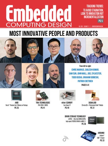
TRACKING TRENDS: To Avoid Stagnation, Look to Innovation Not Incrementalization PG 5 FALL 2026 | VOLUME 24 | 2 | EMBEDDEDCOMPUTING.COM
MOST INNOVATIVE PEOPLE AND PRODUCTS
From left to right:
CHRIS MARKUS, SAILESH KUMAR, SAM SUN, JOHN WALL, JOEL SYLVESTER, TODD OUSKA, GRAHAM GOBIESKI, PATRICK DIETRICH PAGES 6-9
AMD
TRIA TECHNOLOGIES
Versal Premium Gen 2 Memory on Package
PG 35
™
TRIA OSM-LF-IMX95
NVENT SCHROFF Easy Swap LFT
C0-microSD+ Professional UxHw® Module
PG 41
PG 44
PG 31
SIGNALOID
BIWIN STORAGE TECHNOLOGY ePoP5X – Ultra-thin BIWIN ePoP5X, high-speed LPDDR5X DRAM & eMMC 5.1
PG 36
ARDUINO Arduino® UNO™ Q board
PG 33
BY ENGINEERS, FOR ENGINEERS In the rapidly changing technology universe, embedded designers might be looking for an elusive component to eliminate noise, or they might want low-cost debugging tools to reduce the hours spent locating that last software bug. Embedded design is all about defining and controlling these details sufficiently to produce the desired result within budget and on schedule. Embedded Computing Design (ECD) is the go-to, trusted property for information regarding embedded design and development.
embedded-computing.com
AD LIST PAGE
ADVERTISER
1
AMD
1
Arduino
6
Baya Systems
1,6
Biwin Technology
9
BlackBerry QNX
7
Bootloop
TECHNOLOGY EDITOR Curt Schwaderer curt.schwaderer@opensysmedia.com
7
Connect Tech (Heico Corporation)
CREATIVE DIRECTOR Stephanie Sweet stephanie.sweet@opensysmedia.com
8
Dukosi Ltd
8
Efficient Computer
48
IQPC Exhibitions – Where the UK Microelectronics Ecosystem Converges
EDITOR IN CHIEF Ken Briodagh ken.briodagh@opensysmedia.com ASSISTANT MANAGING EDITOR Tiera Oliver tiera.oliver@opensysmedia.com PRODUCTION EDITOR Chad Cox chad.cox@opensysmedia.com CONTRIBUTING EDITOR Rich Nass rich.nass@opensysmedia.com
WEB DEVELOPER Paul Nelson paul.nelson@opensysmedia.com EMAIL MARKETING SPECIALIST Drew Kaufman drew.kaufman@opensysmedia.com WEBCAST MANAGER Marvin Augustyn marvin.augustyn@opensysmedia.com
1
nVent SCHROFF
DIRECTOR OF SALES Tom Varcie tom.varcie@opensysmedia.com (734) 748-9660
13
STRATEGIC ACCOUNT MANAGER Bill Barron bill.barron@opensysmedia.com (516) 376-9838
PICO Electronics Inc – New AVP/AVN Series
1
Signaloid
1
Tria Technologies
9
wolfSSL
SALES/MARKETING
EAST COAST SALES MANAGER Bill Baumann bill.baumann@opensysmedia.com (609) 610-5400 SOUTHERN CAL REGIONAL SALES MANAGER Len Pettek len.pettek@opensysmedia.com (805) 231-9582 DIRECTOR OF SALES ENABLEMENT Barbara Quinlan barbara.quinlan@opensysmedia.com AND PRODUCT MARKETING (480) 236-8818 INSIDE SALES Amy Russell amy.russell@opensysmedia.com STRATEGIC ACCOUNT MANAGER Lesley Harmoning lesley.harmoning@opensysmedia.com EUROPEAN ACCOUNT MANAGER Jill Thibert jill.thibert@opensysmedia.com EUROPEAN ACCOUNT MANAGER Michael O’Kane michael.okane@opensysmedia.com TAIWAN SALES ACCOUNT MANAGER Patty Wu patty.wu@opensysmedia.com CHINA SALES ACCOUNT MANAGER Judy Wang judywang2000@vip.126.com
SOCIAL
Facebook.com/Embedded.Computing.Design
@Embedded_comp
WWW.OPENSYSMEDIA.COM
CO-PRESIDENT Patrick Hopper patrick.hopper@opensysmedia.com CO-PRESIDENT John McHale john.mchale@opensysmedia.com DIRECTOR OF OPERATIONS AND CUSTOMER SUCCESS Gina Peter gina.peter@opensysmedia.com GRAPHIC DESIGN MANAGER Kaitlyn Bellerson kaitlyn.bellerson@opensysmedia.com FINANCIAL ASSISTANT Emily Verhoeks emily.verhoeks@opensysmedia.com SUBSCRIPTION MANAGER subscriptions@opensysmedia.com OFFICE MAILING ADDRESS 3120 W Carefree Highway, Suite 1-640 • Phoenix AZ 85087 • Tel: (480) 967-5581 REPRINTS WRIGHT’S MEDIA REPRINT COORDINATOR Marcia Brewer mbrewer@wrightsmedia.com (281) 419-5725
www.embeddedcomputing.com
www.linkedin.com/showcase/ embedded-computing-design/
www.youtube.com/c/ EmbeddedComputingDesign
EMBEDDED COMPUTING DESIGN ADVISORY BOARD Ian Ferguson, Lynx Software Technologies Jack Ganssle, Ganssle Group Bill Gatliff, Independent Consultant Andrew Girson, Barr Group David Kleidermacher, Google Jean LaBrosse, Independent Consultant Scot Morrison, Siemens Digital Industries Software Rob Oshana, NXP Kamran Shah, Klick Health
Embedded Computing Design with MOST INNOVATIVE PEOPLE AND PRODUCTS | Fall 2026
3
CONTENTS
Fall 2026 | Volume 24 | Number 2
FEATURES 10 How Synthetic DNA for Data Storage 14 Advancing Flash Memory Performance By Sérgio Silva, Ramesh Hanchinal, and Bruno Trematore
18 A Co-Development for the
AI Age: AtlasBase and imec’s Integrated Chip for DNA-Based Data Storage By Tiera Oliver, Assistant Managing Editor
20 The Thermal Efficiency Revolution:
Profiles for the Most Innovative Person begin on page 6.
Why Data Centers Are Rethinking PCB Design
By Lou Farrell, Senior Editor of Computing, Revolutionized Magazine
How Synthetic DNA for Data Storage Could Help the Memory Crisis
Protection Device for Your Next Design By Paulius Juskevicius, Business Development Manager, Littelfuse
Tune In: https://embeddedcomputing.com/ technology/storage/how-synthetic-dna-fordata-storage-could-help-the-memory-crisis-2
26 Raspberry Pi and Arduino for Industrial
ICYMI Ep 62: Arm, Qualcomm, NVIDIA, Siemens, Synopsys
Applications
By Giampiero Baggiani Co-Founder, Head of Software Development, Sfera Labs
20
By Sarah Zalusky, Software Architect & Engineering Leader, JKI
26
COLUMN TRACKING TRENDS
To Avoid Stagnation, Look to Innovation Not Incrementalization By Ken Briodagh, Editor-in-Chief
4
Watch Now: https://embeddedcomputing. com/application/tech-news-roundup/icymi-ep62-arm-qualcomm-nvidia-siemens-synopsys
Embedded Executive: Keep Your Network Up To Date, Regardless of Its Age | Digi International
Tune In: https://embeddedcomputing.com/ application/industrial/industrial-computing/ embedded-executive-keep-your-network-up-todate-regardless-of-its-age-digi-international
6 2026 MOST INNOVATIVE PEOPLE
5
WEB EXTRAS
14
22 How to Choose the Best Overcurrent
30 2026 MOST INNOVATIVE PRODUCTS
bit.ly/ECDYouTubeChannel
Incremental improvements do not stave off the dangers of stagnation, nor are they the same thing as innovation. Here in our fall resource guide, also our innovation issue, we’ve featured eight industry executives and engineers who have created a culture that encourages innovation and have often been instrumental in inventing such innovations themselves.
for the Edge AI Era
Every LabVIEW Team Should Be Thinking About
@embedded_comp
COVER
By Tiera Oliver, Assistant Managing Editor
28 Three Pillars of Software Security
@Embedded.Computing.Design
www.instagram.com/embeddedcomputingdesign
10
Could Help the Memory Crisis
opsy.st/ECDLinkedIn
Published by:
2026 OpenSystems Media® © 2026 Embedded Computing Design All registered brands and trademarks within Embedded Computing Design magazine are the property of their respective owners. ISSN: Print 1542-6408 Online: 1542-6459
To unsubscribe, email your name, address, and subscription number as it appears on the label to: subscriptions@opensysmedia.com
Embedded Computing Design with MOST INNOVATIVE PEOPLE AND PRODUCTS | Fall 2026
www.embeddedcomputing.com
TRACKING TRENDS
ken.briodagh@opensysmedia.com
To Avoid Stagnation, Look to Innovation Not Incrementalization By Ken Briodagh Editor-in-Chief I want to begin by saying that there is nothing wrong with incremental improvements. These tweaks and improvements from version to version are the heart and soul of engineering and have always been. Finding a new timing that makes a straight six engine run as efficient as any four-banger without sacrificing power or introducing the terrible turbocharger (I hate a turbo) would be a revolution of an incremental improvement. But incremental improvements do not stave off the dangers of stagnation, nor are they the same thing as innovation. Innovation, in my opinion, is the moment when a leap of creativity is added to an engineering (or other) problem and the result is not a “better widget” but an entirely new process, solution, material, or answer than has ever been tried before. The steam engine is an example of such an innovation. As is agriculture or nuclear energy or the internet (talk about a case for incremental destruction amirite?). Now, this is our fall resource guide, but it’s also our innovation issue and we’ve featured eight industry executives and engineers who have created a culture that encourages innovation and often have been instrumental in inventing such an innovation themselves.
companies, instead of thinking about the next gamechanging solution that the industry needs. I’m certainly not blaming you engineers and developers here. This is a problem coming from the top down. Many of you execs need to take a page out of the books of our innovators in this issue and start letting your engineers innovate and invent. You’re scared of risk and terrified that an invention will be Betamax instead of VHS, but you get no chance to invent VHS if you never try. The world’s best and most advanced 8-track can’t ever sound as clear as a CD, even if it comes with your very own pair of scissors to edit songs at home. Yes, this is a call out. And a challenge. I dare you to get brave and give your engineering teams one directive: invent something. No one needs you to add another 3GB of RAM and call it a new model. What we need is a new solution for memory that doesn’t rely on the old methods. See Tiera Oliver’s two-part series on just that in this issue. What we need are energy storage and transmission solutions that make sustainable energy from solar and wind more viable and reliable.
As one example, I’ll point out Joel Sylvester, Founder and CTO of Dukosi, because he’s working in an area that I think is in desperate need of that innovation inflection point: battery. He and the team at Dukosi are advancing battery technology and sustainable electrification and the company’s Cell Monitoring System is a key innovation.
What we need is innovation instead of incrementalization. What we need is leadership that isn’t so risk-averse that they’ve failed to meet the needs of the marketplace. And if we don’t get that kind of thinking soon, across the whole industry, we’re going to keep stagnating and finding customers who don’t see the point of changing or upgrading. What’s worse is that we’re very likely to start seeing the forced obsolescence that’s poisoning the consumer electronics space start to enter the well of industrial computing.
That’s just a taster from one of the eight leaders in our feature, so get over there and check it out.
Now, that’s a terrifying thought when you consider the systems we work on.
I’ve ranted recently on both our Embedded Insiders podcast and my weekly news show on YouTube ICYMI (subscribe to both today!) that the technology space is particular is, I think, at great risk of stagnation because of an obsession with incremental improvement over innovation. Putting out the next version or added “feature” has become the driving force of engineering in far too many
CTOs, this is a direct call to action for you. You know if you’re not driving the kind of risk taking that leads to invention and innovation. You also know if your development team is being hampered by cowardly leadership, and I’m giving you permission to start making noise about it.
www.embeddedcomputing.com
Embedded Computing Design with MOST INNOVATIVE PEOPLE AND PRODUCTS | Fall 2026
5
EMBEDDED COMPUTING DESIGN MOST INNOVATIVE PERSON
SAILESH KUMAR
Chief Executive Officer, Baya Systems
ADVERTORIAL
A seasoned expert in SoC, fabric, I/O, memory architecture, and algorithms, Sailesh Kumar is recognized as one of the authorities in Networking, and in particular, Network on Chip design. While he led industry-first initiatives like the 400G network processor at Huawei, and redefining Xeon architecture transportation at Intel, he’s really known for his serial entrepreneurship in founding software-defined fabric company, Netspeed (acquired by Intel), and more recently, software-defined chiplet platform development company, Baya Systems. He has also authored more than two dozen highly cited papers and holds over 150 patents. Under Sailesh’s leadership, Baya emerged from stealth in June 2024 with software-driven, chiplet-ready technology to reduce design risk and accelerate time to market for complex SoCs and chiplets. The platform enables more than 4 TB/s throughput in complex single-die CPU clusters and multi-petabyte-per-second throughput in multi-chiplet AI designs. Baya raised $36+ million in Series B financing in January 2025, and by mid-2025, Baya reported 5x growth in design wins, with EE Times later describing a dozen new design wins and a rapid growth in headcount to keep pace.
movement and the memory wall through high-radix switching with scalable chiplet-ready modular design where each chiplet could support 256 ports each with 1 Tb/s throughput, 2 GHz+ operation, and alignment with AMBA, UALink, UCIe, and Ultra Ethernet. As a result, Baya now boasts partners like Tenstorrent, Semidynamics, OpenChip, Kandou and many others soon to be announced. The market’s response to Sailesh’s vision for scalable, standards-based data movement has been unequivocally positive, reinforcing Baya’s role in enabling the next generation of AI. Sailesh’s impact makes scalable, standards-aware data movement a foundational advantage for the next generation of embedded, intelligent compute systems.
Sailesh is the visionary behind Baya’s first-of-its-kind NeuraScale fabric, which promises to radically improve AI challenges in data-
www.bayasystems.com
EMBEDDED COMPUTING DESIGN MOST INNOVATIVE PERSON ECD BayaSystems-SaileshKumar - Profile MostInnov July26 HP.indd 1
8/11/26 9:23 AM
SAM SUN
Chairman, BIWIN Storage Technology Co., Ltd.
As the Chairman of BIWIN Storage Technology Co., Ltd., Sam Sun has demonstrated outstanding strategic foresight and innovation-driven leadership, guiding BIWIN’s transformation for the AI era. A graduate from Oxford Brookes University in the UK, he has successfully led BIWIN’s change from a traditional storage R&D and manufacturing company into a system-level solutions provider focused on “Advanced Storage + Advanced Packaging.”
some of the world’s leading brands and are widely applied globally in AI edge devices, servers, PCs, smartphones, robots,and automotives. Through leadership in technology innovation and ecosystem development, Sam Sun continues to contribute to the advancement of China’s semiconductor storage industry and the future of intelligent computing.
ADVERTORIAL
Sam Sun strategically established an integrated innovation model encompassing IC design, storage solution development, advanced packaging, and proprietary testing capabilities, creating differentiated technological advantages and strengthening the company’s competitiveness across the global semiconductor ecosystem. Driven by continuous investment in R&D and strategic industry collaboration, he has expanded BIWIN’s global presence and overseen the company’s entry on the SSE STAR 50 Index. Under his direction, BIWIN’s products now serve the supply chains of
6
www.biwintechnology.com
Embedded Computing Design with MOST INNOVATIVE PEOPLE AND PRODUCTS | Fall 2026
www.embeddedcomputing.com
EMBEDDED COMPUTING DESIGN MOST INNOVATIVE PERSON
CHRIS MARKUS
Co-Founder and CTO, BootLoop
As Firmware Lead for the Raptor engine and Software Lead for the Starship booster catch at SpaceX, Chris Markus was instrumental in turning firmware validation from a highly manual process into a fully-automated pipeline where passing tests could clear firmware for deployment to the vehicle. Chris and his team brought a stepchange in rigor to the firmware workflow which support the company’s successes to this day.
ADVERTORIAL
That experience also showed Chris how different the reality remains for most firmware teams. Firmware development and validation is still a game of edge cases, fragile test benches, and bottlenecks on an individual’s hoarded knowledge. These constraints lead to the all-too-predictable delayed product releases, fielded defects, and recalls.
First at SpaceX and now at BootLoop, Chris has built what the embedded industry didn’t yet know it needed: firmware HIL and CI at the frontier of hardware engineering, and now a new foundation for AI-assisted embedded development built on accessible bench orchestration, intuitive yet powerful test setup and orchestration capabilities, and hardware-aware AI. This time, however, BootLoop has made that infrastructure accessible, putting frontier-grade embedded capabilities within reach of teams that cannot spend years building their own.
Building BootLoop, Chris has changed the calculus for all firmware and hardware businesses. BootLoop makes physical validation easier to set up, reproduce, and scale, while maintaining system-level context across schematics, datasheets, source code, test infrastructure, and measured results. It combines deterministic testing on real hardware with hardwareaware code generation, shortening the path from a firmware change to evidence that it works.
www.bootloop.ai
EMBEDDED COMPUTING DESIGN MOST INNOVATIVE PERSON ECD BootLoop-Chris Markus - Profile MostInnov July26 HP.indd 1
8/11/26 9:23 AM
PATRICK DIETRICH
President, Connect Tech
Patrick Dietrich, P.Eng., President of Connect Tech, built his reputation transforming emerging technology into real-world solutions. His fascination with computers started at six years old, and over a nearly two-decade climb through technical support, hardware design, and CTO, he developed a leadership style that’s customer-focused, engineering-driven, and relentlessly committed to solving complex problems.
ADVERTORIAL
Dietrich recognized the potential of Edge AI long before it became mainstream. Over the past two decades he’s guided Connect Tech through multiple generations of accelerated computing, from discrete-GPU rendering to GPGPU computing to today’s Edge AI and Physical AI platforms, evolving the company from a traditional embedded computing shop into a global leader in Edge AI. Central to that shift was Connect Tech’s early, strategic partnership with NVIDIA, struck years before the market caught up. In 2025, that vision culminated in CTai LABS, Connect Tech’s fullstack AI engineering team, built to help robotics, machine vision, and autonomous systems companies bring AI solutions to market faster by combining integration, embedded engineering, firmware, and model optimization under one roof. www.embeddedcomputing.com
As Founder, Mentor, and predecessor David J. Worthen explains, “Patrick has a rare combination of deep technical knowledge and the ability to inspire people around him. I couldn’t be more confident in the future he’s building.” A licensed Professional Engineer and a familiar presence at Embedded World, XPONENTIAL, electronica, Humanoids Summit, and NVIDIA GTC, Dietrich remains deeply engaged with the technologies shaping intelligent systems. “The future of AI won’t be defined by models alone,” says Dietrich. “It will be defined by how effectively they’re deployed in the real world. Our engineering expertise allows us to bridge that gap, transforming complex customer challenges into reliable Edge AI solutions.”
connecttech.com
Embedded Computing Design with MOST INNOVATIVE PEOPLE AND PRODUCTS | Fall 2026
7
EMBEDDED COMPUTING DESIGN MOST INNOVATIVE PERSON
JOEL SYLVESTER
ADVERTORIAL
Founder and Chief Technology Officer, Dukosi
Dukosi was founded in 2003 by Joel Sylvester as a silicon chip design services company, and in 2013 made a strategic move to focus the company on developing battery technology to transform the performance, safety, and sustainability of batteries powering the next generation of electric vehicles (xEV), industrial transportation and battery energy storage systems. Joel’s dedication to advancing battery technology and sustainable electrification has been the driving force behind the company’s innovative and award winning Dukosi Cell Monitoring System (DKCMS®) and C-SynQ® communication protocol. He is the key inventor of Dukosi’s innovative system architecture and communications technology, and holds 21 patent families. He engages in joint research projects with academia and industry consortia, investigating new technologies and anticipating drivers that can help accelerate adoption of electrification and propel the industry forward. Joel frequently presents at technology conferences and battery industry events, sharing his experience and know-how in solving some of the battery industries longstanding challenges for improving battery performance, safety and reliability at lower system cost.
was foundational in creating Dukosi’s unique smart cell monitoring solutions. The intelligent chip-on-cell technology and the C-SynQ® communications protocol that he invented is transforming the way batteries are designed, monitored and managed – advancing his earliest vision to have Dukosi technology powering every battery cell in the transition to electrification. Seeing the limitations of existing wired and wireless BMS approaches, Joel developed Dukosi’s novel contactless solution, freeing up design constraints to provide greater safety, design flexibility and scalability. The use of an SoC architecture, integrating measurement, processing, communications and storage anticipated the industry drive towards providing lifetime traceability, enabling customers’ products to be compliance-ready for digital product passports and regulations like the EU Battery Passport.
With his background in semiconductor design, embedded systems and the application of System-on-Chip (SoC) to battery systems, Joel
www.dukosi.com
EMBEDDED COMPUTING DESIGN MOST INNOVATIVE PERSON Dukosi-JoelSylvester - Profile MostInnov July26 HP.indd 1
8/11/26 9:23 AM
GRAHAM GOBIESKI
Co-Founder & Chief Technology Officer, Efficient Computer
Graham Gobieski, co-founder and Chief Technology Officer of Efficient Computer, did something the semiconductor industry had largely stopped attempting: he questioned the foundation every processor is built on, then built a better one.
ADVERTORIAL
Nearly every processor in production still follows the same fetchdecode-execute model from the 1940s, an approach that spends most of its energy moving instructions and data rather than computing. During his doctoral research at Carnegie Mellon University, Graham asked why devices at the edge of the network, the ones that most need to run for years on a battery, were stuck with that overhead. His answer became the Fabric architecture, a spatial dataflow design that keeps values close to compute and eliminates the energy wasted on constant instruction fetch.
with the effcc Compiler. No rewrites, no proprietary lock-in, no accelerator-style constraints. That combination reflects Graham’s rarest quality. Most architecture innovations demand that the world change around them. Graham designed hardware and software in sync from day one, so a fundamentally new machine arrives looking standard everywhere else. It opens computing frontiers, from always-on sensing to autonomous drones, that were previously walled off by energy budgets. Innovation isn’t incremental improvements. It is the courage to start over on an 80-year-old assumption and the discipline to carry that idea from a PhD thesis to working silicon. Graham did both.
That research is now shipping in silicon. As CTO, Graham led the Fabric architecture development from academic papers to the Electron E1 general-purpose processor, delivering up to 100x greater energy efficiency on real workloads. Just as important is what he refused to trade away: developers keep their existing C and C++ code, which compiles immediately
8
www.efficient.computer
Embedded Computing Design with MOST INNOVATIVE PEOPLE AND PRODUCTS | Fall 2026
www.embeddedcomputing.com
EMBEDDED COMPUTING DESIGN MOST INNOVATIVE PERSON
JOHN WALL
QNX, President
ADVERTORIAL
John Wall, President of QNX, is the driving force behind one of the embedded software industry’s most significant transformations. Since taking the helm in November 2025, and across more than three decades with QNX, John has consistently championed innovation, reshaping how safety-critical systems are built for the modern world. Under John’s guidance, QNX has continued to grow beyond its automotive leadership into markets such as industrial automation and robotics, positioning the company at the forefront of the emerging Physical AI and software-defined systems era. In his various roles at QNX, John has overseen the planning, design and development of a portfolio that gives customers the ability to innovate faster while meeting the most demanding standards for safety and security. He has also been pivotal in the introduction of QNX Everywhere, the initiative that gives developers, students and educators free, non-commercial access to the QNX Software Development Platform, recognizing that democratizing access to production-grade tools will help grow the next generation of embedded talent. What sets John apart is his ability to pair deep technical expertise with forward-looking vision. Having joined QNX in 1993 and
progressed through engineering, services, product and operations leadership roles, he understands innovation from the ground up. This grounding informs his advocacy on the issues shaping the industry’s future; from software-defined vehicles and functional safety to evolving regulatory frameworks, he is a sought-after voice at industry forums worldwide and helps set the agenda for how embedded software underpins the next generation of intelligent machines. A graduate of Carleton University with a Bachelor of Engineering in Electrical and Electronics, John combines engineering rigour with commercial ambition. His focus on solving hard problems, empowering teams and anticipating where technology is heading makes him a truly deserving nominee for the Most Innovative People award.
www.qnx.software
EMBEDDED COMPUTING DESIGN MOST INNOVATIVE PERSON QNX-JohnWall - Profile MostInnov July26 HP.indd 1
8/11/26 9:22 AM
TODD OUSKA
Co-Founder and CTO, wolfSSL
For more than two decades Todd Ouska has anticipated the security challenges embedded engineers would face next and turned complex cryptographic requirements into software they can actually deploy.
ADVERTORIAL
He co-founded wolfSSL with Larry Stefonic in 2004 on a premise the industry had not yet accepted: OpenSSL existed, but embedded developers needed an alternative built for their constraints. It had to be smaller, faster, portable across non-standard toolchains, and wrapped in a clean, modern API. Todd turned that premise into an open-source, dual-licensed product with commercial support and OpenSSL compatibility, giving embedded teams a migration path instead of a rewrite. As CTO, Todd has driven wolfSSL well beyond TLS into a full embedded security portfolio that now includes TLS and DTLS, FIPS 140-3 validated cryptography, secure boot, TPM 2.0, automotive HSM firmware, a deterministic TCP/IP stack, and post-quantum cryptography. That code runs anywhere, from bare metal to mainframes, in markets as varied as automotive ECUs, medical devices, avionics, and critical infrastructure. Today wolfSSL secures more than 5 billion connections. That portfolio consistently arrives early. Under Todd’s technical direction, wolfSSL delivered the first commercial implementation of TLS www.embeddedcomputing.com
1.3 and earned the world’s first SP800-140Br1-compliant FIPS 140-3 validation, evidence that he moves emerging standards out of the specification and into production inside real memory, performance, hardware, and certification budgets. His innovation is disciplined by the constraints his users live with: fixed memory budgets, hard real-time deadlines, hardware that varies program to program, and product lifecycles measured in decades. Solving cryptography under those conditions is a different problem than solving it on a server, and Todd has solved it repeatedly. Technical foresight, early execution on emerging standards, and cryptography built for the industry’s hardest constraints: that combination makes Todd one of embedded security’s most innovative engineers.
www.wolfssl.com
Embedded Computing Design with MOST INNOVATIVE PEOPLE AND PRODUCTS | Fall 2026
9
NEXT-GENERATION DATA STORAGE
How Synthetic DNA for Data Storage Could Help the Memory Crisis By Tiera Oliver, Assistant Managing Editor If you haven’t already heard, we’re in a memory crisis. More specifically, we’re in a global memory chip short-age, which began in late 2025 and is likely to persist into 2027, according to the International Data Corporation1.
T
his shortage is caused by the exponential increase in high-performance AI models and the amount of data and subsequent data centers required to keep them running. AI models come in a wide range of sizes, speeds, costs, and capabilities. There are small, lightweight AI models that run locally on devices for quick processing, such as AI assistants, and large, foundational models designed for powerful, long-form reasoning and coding use cases, such as code generation and analysis.
10
The challenge is that AI is hungry for memory, and regardless of how small the type of AI memory is, there are still billions of devices to feed. With both small and large models, there’s not just one that takes precedence over the other; they are both advancing and consuming at the same speed. This causes
Embedded Computing Design with MOST INNOVATIVE PEOPLE AND PRODUCTS | Fall 2026
www.embeddedcomputing.com
NEXT-GENERATION DATA STORAGE
FIGURE 1: DNA thin films seen under optical microscopy.
an increased need for DRAM, NAND flash, and HBM memory types, and even these have their limits. Thanks to some leading-edge research in Biology, there might be a solution forthcoming. Using Biology to Increase Capacity Kavya S. Keremane is a postdoctoral researcher in materials science and engineering at Penn State. Her research background is in optoelectronics and photovoltaics, especially in energy storage and conversion, memory storage, and biomimetic sensing. Keremane’s current research focus is on DNA semiconductor-based memory storage device development and fabrication, which can support the development of ultra-low power next-generation memory devices. (Figure 1) Most engineers are familiar with the traditional types of memory, like flash and DRAM, but Keremane’s research makes use of biological material that functions differently from the former silicon-based types. “Synthetic DNA data storage is a technological process that uses artificially or customized synthetic DNA molecules where we can store the data or information. Traditionally, computers store information using bits, where each position can be either 0 or 1, so only one piece of information per position,” said Keremane. “In the case of DNA, we have 4 nucleobases or four building blocks, called adenine, guanine, thymine, and www.embeddedcomputing.com
FIGURE 2: Two 90-degree views of the DENSS envelope overlay with the dimer of the DNA hairpin.
cytosine. Because there are more choices, each position in DNA can hold more information than a single bit.” This concept goes back to the human body and how all genetic information is stored in our DNA. Most cells in the human body contain a nucleus, which houses genetic material, and the human genome has around 3.2 billion base pairs. This means that our bodies hold almost 1 gigabyte of information. (Figure 2) “So, DNA provides both a greater possibility for compression and orders of magnitude more physical density for data storage due to its molecular characteristics, and the fact that it is a 3D storage method,” explained Keremane. Keremane works alongside Dr. Bed Poudel, a research professor of materials science and engineering at Penn State University, whose research focuses on energy materials. Dr. Poudel said the challenges in current data storage technology, especially with AI chips, are energy consumption per process and storage density. He explained that the goal of their research is propelled by the demand for higher computing power and, therefore, the need to store more data. They’re working to support the need for higher data storage with lower energy. According to Dr. Poudel, they are working to solve a “major problem with AI chips and computation ... the more energy you consume, the chips get hotter. So, in this process, we are using a lot less energy, 100 times less ... so that way, the thermal management problem would be a lot simpler. So, the data storage center, they can they can operate, let’s say, more comfortably, right?” The Biological Benefits and Challenges In addition to addressing the challenges of energy consumption and thermal management, the hybrid DNA solution supports improved density and durability compared to existing silicon-based storage media. In their research, Keremane and Dr. Poudel’s hybrid DNA, along with perovskites between platinum and silver, use a similar architecture to traditional commercial devices. (Figure 3)
Embedded Computing Design with MOST INNOVATIVE PEOPLE AND PRODUCTS | Fall 2026
11
NEXT-GENERATION DATA STORAGE
According to the Clean Energy Institute at the University of Washington, “A perovskite is a material that has the same crystal structure as the mineral calcium titanium oxide, the first-discovered perovskite crystal.” The high-performance hybrid semiconductor material used in this research is made up of organic-inorganic halide perovskites (OIHPs), with the structure ABX3, where A is an organic cation, B is a metal (Pb, Sn), and X is a halide.
FIGURE 3: (a) Schematic illustration of the resistive memory device structure, (b) Cross-sectional SEM images of Ag/(PEA)2(MA)Pb2I7/Ag-synDNA/Pt memristors, and (c) Schematic illustration of the interaction between Ag-synDNA and quasi-2D perovskite.
Keremane said, “In today’s engineered devices, like the DNA-perovskite memristors described in our paper, DNA is not used to store data as sequences but as a functional material within electronic components. It helps control charge transport and enables low-power, nonvolatile memory operation ... we can design the hardware which can mimic the biological neural networks to get a more efficient and more efficiency as well as speed in artificial intelligence tasks. So, these DNA-based data storage systems can lead to a long-term neuromorphic computing hardware solution, as well as some bio-integrated electronics.” “They are crystals in the form of ABX3. That means we can combine different organic cations, inorganic cations, metal ions, and halides. And we can design their composition and play with different metal ions to reform the structure ... we used two-dimensional perovskites here for our work, and these materials have excellent charge transport properties, ionic conductivity, and band gap can be used based on the compositions. And
OpenSystems Media works with industry leaders to develop and publish content that educates our readers. Building the Next Generation of Resilient Industrial Analyzers Servomex, a global leader in gas analysis, partnered with QNX and NXP to modernize its next-generation industrial analyzers for safety-critical environments. Facing increasing demands for precision, reliability, and resilience in complex applications, Servomex adopted the QNX real-time operating system and the NXP i.MX93 processor to build a scalable, secure, and high-performance embedded platform. Leveraging QNX’s microkernel architecture and proven realtime capabilities, Servomex enhanced system availability, strengthened cybersecurity, and accelerated development of future-ready products. The result is a robust software and hardware foundation that enables continuous, high-accuracy gas analysis in demanding industries such as energy, chemicals, and manufacturing. https://embeddedcomputing.com/application/industrial/ smart-energy-utilities/building-the-next-generation-of-resilient-industrial-analyzers
12
Check out our white papers at www.embedded-computing.com/ white-paper-library
Embedded Computing Design with MOST INNOVATIVE PEOPLE AND PRODUCTS | Fall 2026
www.embeddedcomputing.com
the performance mainly depends on the crystal quality and the compositions here,” explained Keremane. But of course, a solution as innovative as this still has its challenges. Combining such delicate biological material with electronics that are often built to be durable for rugged environments presents integration issues because DNA is not compatible with existing semiconductor fabrication. DNA can degrade under high temperatures, which affects manufacturing. Dr. Poudel said, “This technology is so drastically different from the existing technology … traditionally chips have been made in a certain way, but I think this is very different: nature-inspired, using DNA ... the biggest thing is, right now this is the early stage, so there needs to be probably some resource and investment from the companies to adapt this process into their existing system. So that will be, I think, one of the main challenges before we see this into commercial product.” The Future of DNA-Based Data Storage Investment would be beneficial since the cost of current DNA synthesis is too expensive for large-scale data storage and manufacturing. DNA-based storage is still in the early stages of research, especially with the care that needs to go into the design and customization of products. “As the demand for low-power data storage grows, especially with AI and data centers, there is strong motivation to develop these technologies further. In the future, if DNA storage becomes commercial and scalable, the cost is expected to come down,” said Keremane. “In the short term, we will likely see improved prototypes with better stability, endurance, and integration, especially in hybrid systems like DNA-semiconductor memristors, where molecular design is used to control electronic behavior more precisely.” Dr. Poudel and Keremane said they have been in contact with companies to discuss how synthetic DNA can be made with chip-level integration. They’ll www.embeddedcomputing.com
continue to move toward large proposals through the government to accelerate the process. They have already begun lab innovation, so what’s next is partnering with companies and governments to be able to introduce more viable prototypes and bring this vision to reality. Keremane said, “For lower power consumption data storage and media, DNA data storage is an excellent option. There are many companies working commercially to customize the DNA and increase the slow writing speeds in data storage. So, it’s in high demand right now. I think in five to 10 years, we can see a drastic change in improvement or progress in the DNA-based data storage media.” References
1. https://www.idc.com/resource-center/blog/global-memory-shortage-crisis-market-analysis-andthe-potential-impact-on-the-smartphone-and-pc-markets-in-2026/ B58_Island_4_625x7.qxp_Layout 1 7/9/26 1:19 PM Page 1
AS9100D ISO 9001:2015
NEW AVP/AVN SERIES! 10,000 VDC OUTPUTS
• Isolated • High Reliability • 6,000, 7,000, 8,000, 9,000, 10,000 VDC, positive and negative output models • 1.25 watt output power, -25 to +70C operating temperature standard, no de rating • 5-12-15-24 and 28 VDC inputs standard • Military Upgrades Available Expanded operating temperature, -55 to + 85C available - Selected MIL-STD-883 screening available • Free review of any additional requirements and specifications you may have to comply with • Fully encapsulated for use in harsh environmental conditions USA & Canada: 800-431-1064 Worldwide: +1-914-738-1400
E Mail: info@picoelectronics.com
Embedded Computing Design with MOST INNOVATIVE PEOPLE AND PRODUCTS | Fall 2026
13
MEMORY & STORAGE STANDARDS
Advancing Flash Memory Performance for the Edge AI Era By Sérgio Silva, Chair of the MIPI M-PHY Working Group Ramesh Hanchinal, Chair of the MIPI UniPro Working Group Bruno Trematore, Co-Chair of the JEDEC UFS Technical Group As embedded systems evolve to support more powerful edge AI, real-time analytics and high-resolution video processing, flash memory storage has become a critical determinant of system performance, responsiveness and power efficiency. In the past, flash memory developments focused primarily on increasing capacity and reducing cost. Today bandwidth, latency, reliability, capacity and cost are all equally important design criteria.
14
Embedded Computing Design with MOST INNOVATIVE PEOPLE AND PRODUCTS | Fall 2026
www.embeddedcomputing.com
MIPI Alliance www.mipi.org
JEDEC UFS Technical Group https://www.jedec.org/
https://www.linkedin.com/company/mipi-alliance
YOU TUBE
www.youtube.com/user/MIPIAlliance
MEMORY & STORAGE STANDARDS
T
his article describes how three updated specifications, MIPI M-PHY v6.0, MIPI UniPro v3.0 and JEDEC UFS 5.0 support these new design challenges. (Figure 1). It will explain how they deliver a high-performance flash memory storage solution that addresses the growing market need for high-throughput, lowlatency flash memory in embedded platforms, with use cases ranging from mobile, PC and gaming devices to automotive and industrial systems.
FIGURE 1: Use of MIPI M-PHY and MIPI UniPro within JEDEC UFS (Source: MIPI Alliance)
Faster Physical Layer Supports Double the Bandwidth MIPI M-PHY v6.0 serves as the foundation of the updated solution, introducing a significant advancement in physicallayer performance. Adopting PAM4 signaling combined with 1b1b encoding, M-PHY v6.0 adds a new speed gear – Gear 6 – which enables data rates of up to 46.6 Gbps per lane. This is double the bandwidth of the previous version of the specification while also maintaining backward compatibility. The increase in data rate is not only about peak throughput; it enables new design trade-offs, such as the ability to reduce lane count to save pins and reduce power while maintaining the required level of bandwidth. M-PHY’s support of burst-mode operation and ultra-lowpower standby states are also critical for energy-constrained designs, particularly for battery-powered systems. The introduction of new signal integrity features is also highly beneficial. Optional link equalization and training features, together with advanced transmitter and receiver equalization schemes, will enable systems to maintain reliable high-speed operation in noisier electromagnetic environments. This is particularly advantageous with challenging designs, such as the channels required for long PCB traces or compact, highdensity packages. In addition, new diagnostic capabilities like eye monitoring will help reduce system debug complexity. www.embeddedcomputing.com
FIGURE 2: MIPI M-PHY and MIPI UniPro specification evolution (Source: MIPI Alliance)
A More Efficient, Reliable Link Layer Leveraging the M-PHY physical layer, MIPI UniPro v3.0 introduces several new enhancements that improve transport and link-layer efficiency. Supporting 46.6 Gbps per lane, UniPro v3.0 aligns with M-PHY’s new high-speed data-rate, while also improving data integrity and reducing signaling overhead. (Figure 2). A major update is the introduction of 1b1b encoding at HS-G6 instead of 8b/10b encoding and reducing signaling overhead by approximately 20%. This is complemented by a new transport framing structure, along with Reed-Solomon forward error correction and 64-bit CRC protection, enabling extremely low bit-error rates suitable for safety-critical applications. UniPro v3.0 also introduces several new capabilities that help optimize link management. These include faster link startup, mandatory high-speed link initialization and new streamlined power mode transitions all of which help reduce latency during system boot-up. In addition, new enhanced link training and equalization procedures
Embedded Computing Design with MOST INNOVATIVE PEOPLE AND PRODUCTS | Fall 2026
15
MEMORY & STORAGE STANDARDS
will enable software-controlled optimization of signal quality, allowing device firmware to adapt to varying channel conditions during system operation. These improvements cement UniPro’s role as a robust link layer that reduces application-layer complexity while also ensuring reliable, high-speed data transport between host and storage devices. UFS 5.0: Ready for the Next Generation of Flash Memory Use Cases JEDEC’s UFS 5.0 standard leverages the numerous advancements provided in M-PHY v6.0 and UniPro v3.0 to deliver the next level of flash memory storage performance. Supporting double the interface bandwidth of UFS 4.0, UFS 5.0 enables faster read/ write operations and reduced latency, delivering improved overall system responsiveness. (Figure 3).
Beyond the raw bandwidth performance, UFS 5.0 also introduces numerous features that enhance firmware and system design. These new features include the addition of zoned storage which reduces write amplification and improves system efficiency by matching logical data placement with the underlying characteristics of flash memory. New pre-erase capabilities will allow host devices to prepare memory blocks in advance of use, minimizing write latency. And a per-command write booster control will enable fine-grained performance tuning for critical workloads. UFS 5.0 also enhances data protection through the addition of inline hashing support in the host controller interface. This capability allows cryptographic operations to be offloaded from the CPU to the memory system, resulting in significantly reduced CPU overhead.
FIGURE 3: Faster boot from UFS due to high-speed sequential read and improved link start-up sequence (estimated, comparative timing shown) (Source: MIPI Alliance)
Hardware-Accelerated Trust: FPGA-Based Secure Networking at 100Gbps As critical infrastructure, AI systems, industrial automation, defense networks, and next-generation communications demand higher bandwidth and lower latency, traditional software-based security architectures are increasingly becoming bottlenecks. The need for deterministic performance, real-time encryption, and resilient communications at 100Gbps is driving a new wave of hardware-accelerated secure networking platforms built on FPGAs. Join AMD and Pantherun for an executive roundtable exploring how FPGA-based architectures are redefining secure communications for modern infrastructure. Watch On Demand: https://resources.embeddedcomputing.com/EmbeddedComputing-Design/hardware-accelerated-trust
WATCH MORE WEBCASTS: www.embedded-computing.com/virtual-events
16
Enabling Edge AI and Data-Intensive Applications A compelling use case for the adoption of UFS 5.0 is the enablement of new or enhanced edge AI capabilities. For example, the large data models used to enable vision-based AI systems often exceed available DRAM capacity, necessitating the efficient loading of these large data models from non-volatile flash storage. The faster and more efficient read/write speeds supported by UFS 5.0 support these new use cases by enabling selective data movement, where the only the necessary portions of the data model are loaded into volatile memory. These new capabilities provided by UFS 5.0 help to balance system performance, power and cost. The release of M-PHY v6.0, UniPro v3.0, and UFS 5.0 marks the next step in the evolution of embedded flash storage. By addressing bandwidth, latency, power and reliability holistically, these specifications enable the next generation of AIenabled embedded systems. As workloads continue to evolve, leveraging the advanced storage stack solution provided by these specifications will be essential to achieving scalable, efficient and futureready designs.
Embedded Computing Design with MOST INNOVATIVE PEOPLE AND PRODUCTS | Fall 2026
www.embeddedcomputing.com
NEWS
ken.briodagh@opensysmedia.com
M&A News Roundup: Embedded Companies are Joining Forces and Making Moves By Ken Briodagh, Editor-in-Chief The embedded industry is rapidly becoming the leader in AI from the Edge to the Data Center, the mind behind the IoT’s ubiquity, and the driver of the semiconductor supply and demand chain. The biggest players are hungry for the innovative ideas that come with acquiring powerful engineering solutions and products through buying smaller companies, and many of them are out making deals to gain that competitive edge. At the end of 2025, the industry shook with the acquisition of Arduino by Qualcomm (look for my recent interview and update on the transition, over on YouTube). Early this year, in February, the momentum continued with the news that TI was set to acquire Silicon Labs for about $7.5 billion in cash. Siemens announced its acquisition of Canopus AI with the stated intention of offering semiconductor manufacturers the ability to “achieve new levels of precision and efficiency in wafer and mask inspection processes.” That’s not all this year either, as GlobalFoundries agreed to acquire Synopsys’ ARC Processor IP Solutions business this spring. The assets and teams are to be integrated with MIPS, and the resulting processor IP suite will be aimed at Physical AI applications. Let’s keep going. Marvell acquired silicon photonics company Polariton this year, too. Marvell said the acquisition strengthens its optical technology portfolio by adding advanced modulation capabilities that enable continued scaling in bandwidth, power efficiency, and integration for next-generation coherent and optical interconnect platforms. Altair completed its exit from Sony Semi and had a big funding round, with a focus on IoT and Physical AI, the company said. Altair’s chipsets power cellular and the LTE-M market in smart cities, energy grids, logistics, vehicle asset trackers, and sports wearables. Altair says its technology is essential to the Physical AI revolution, connecting the physical world of machines and robots to the cloud anywhere across the globe, and connecting AI-powered wearables and consumer devices that require low power, continuous connectivity. As my last example in this incomplete list, Microchip recently signed a definitive agreement to acquire Hailo, a provider of accelerated edge AI processors, advanced vision processing solutions, robotics processors, and comprehensive AI software flows. The transaction should close towards the end of this quarter. The acquisition will expand Microchip’s processing www.embeddedcomputing.com
portfolio for intelligent edge systems and strengthen its ability to deliver accelerated, power-efficient Edge AI solutions for robotics, advanced vision processing and intelligent edge applications, including drones, robots, smart cameras, industrial automation and embedded AI systems. Hailo has spent years demonstrating technology leadership in both Edge AI accelerators and vision-on-chip systems. Its products range from high-performance edge deployments on specialized edge servers with local GenAI and multimodal workloads to low-power vision processing inside a small-form-factor, standalone camera. With Hailo-8, Hailo-10 and Hailo-15, Microchip will gain a portfolio that supports classic computer vision, while adding advanced camera, ISP, DSP, video encoding and AI video stream processing capabilities for intelligent edge systems. The transaction brings a demand-generation engine for edge AI adoption. Hailo’s Raspberry Pi ecosystem, gated Developer Zone, GitHub activity and community forum create a self- sustaining funnel that converts developer engagement into qualified opportunities and customer pipeline. What does all this activity mean? Well, it could mean many things, but in my experience, a slate of big acquisitions in a narrow industry can point to a variety of things. Supply chain uncertainty (we’ve certainly seen that), expectations for future market growth (I don’t think I need to tell you that AI+Embedded+Edge+IoT are all going to equal more semiconductors, everywhere from the data center to the edge), market maturity leading to vertical integration, or most commonly, some mixture of all of the above. And I’m sure you all noticed that most of the above (and all the biggest deals) hinged upon expanding AI capabilities, solutions, and product offerings. What makes sense to me is that this looks like a combination of a maturing US semiconductor manufacturing marketplace, combined with a rapidly growing AI industry bubble (which seems obvious). With all this said, what conclusions can we draw? Since my crystal ball is on the fritz, I’m not going to predict anything. But I’m going to be watching, and so should you, because if 2026 continues this way, the embedded industry might just look substantially different in 12 months. Or even 6. If you see me at embedded world North America, electronica, or CES, come on up and let me know what you’re thinking and seeing out there in the server racks and cloud storage mines.
Embedded Computing Design with MOST INNOVATIVE PEOPLE AND PRODUCTS | Fall 2026
17
NEXT-GENERATION DATA STORAGE
A Co-Development for the AI Age: AtlasBase and imec’s Integrated Chip for DNA-Based Data Storage By Tiera Oliver, Assistant Managing Editor We’re well into the age of AI, where technical advancements are rapidly expanding into varying industries and verticals. But there’s still one caveat to all this expansion: there may not be enough storage.
I
n a previous story, Dr. Kavya S. Keremane, postdoctoral researcher in materials science and engineering, and Dr. Bed Poudel, research professor of materials science and engineering at Penn State University, shared their research in DNA semiconductorbased memory storage device development and fabrication for ultra-low-power nextgeneration memory devices. This research sparked continued interest in exploring which other companies and areas within the industry this could expand into. AtlasBase, formerly known as Atlas Data Storage, a biotechnology company based in San Francisco, California, is accelerating the trend of using commercial DNA sequencers for data storage to improve throughput and cut costs. The trend consists of indexing and error-correction codes (ECC) into each DNA strand.
18
Siraj Nour ElAhmadi, Chief Operating Officer at AtlasBase, says, “At Atlas, we started with a disturbing observation. The fact that humanity is now generating data much faster than any existing medium can keep or can affordably do so.” Artificial Intelligence is without a doubt one of the main drivers in the vast amounts of data generated today. According to Siraj, not only is AI using a lot of data, but, at the same time, it’s
Embedded Computing Design with MOST INNOVATIVE PEOPLE AND PRODUCTS | Fall 2026
www.embeddedcomputing.com
NEXT-GENERATION DATA STORAGE
FIGURE 1: High-density electrode array with 128m sites. (Original image source: www.imec-int.com/en/press/next-generationpermanent-dna-based-data-storage-ai-age)
continuously generating more and more data. This is something he refers to as the “binary tsunami of AI,” which is essentially the hoarding of data. Data has become so valuable to enterprises because it’s believed that over time our ability to process and mine data will improve, so most companies don’t want to just get rid of it. “Atlas was built on a single conviction that molecular or perhaps scientific DNA can become the permanent archival layer for the digital age. That was really the impetus, and that’s our conviction,” says Siraj. “What brought me to Atlas is really this unique combination where we have advanced CMOS and ASIC technology, we have biochemistry, we have synthetic biology, and all coming together under one roof where you usually don’t see that. And it’s really a new type of substrate, a new type of product that we are developing that we believe will solve some of the pressing modernday needs.” This year, AtlasBase and imec, an international research & development organization of nanoelectronics and digital technologies, announced a collaboration to accelerate next-generation, permanent DNA-based data storage for AI. Together, the companies developed an integrated chip that combines a dense nanoscale array of electrochemical cells and a control CMOS ASIC. www.embeddedcomputing.com
FIGURE 2: Process of accelerating digital data storage using synthetic DNA. (Original image source: www.imec-int.com/en/press/next-generation-permanent-dna-based-data-storage-ai-age)
“Over the last 50 years, no other industry, no other technology has achieved the scale and cost reduction than the CMOS and silicon. We basically made that observation, and we married the two. We said, ‘Okay, if we want to get to scale, then we need to anchor our solution on top of CMOS.’ CMOS gives you the scale. Just to give you an example, the hybrid platform that we have today, we call Cleo, has almost 3 billion transistors. It gives us not only the scale, but the precision to control on top of that chip,” Siraj says. The nanoscale electrochemical cell arrays developed by imec are designed to enable programmable DNA synthesis. And according to Simone Severi, Vice President of Research and Development at imec, this concept is nothing new. “The strength of imec is actually in the scaling and in further developing materials and processes to enable scaling. This is a key element for DNA storage because both the synthesis as well as the sequencing need a very aggressively scaled chip, very dense array and very high parallelism in order to be able to bring down the overall cost of the storage device,” says Simone. As we understood in the previous story, with Dr. Kavya S. Keremane and Dr. Bed Poudel, DNA is a breakthrough biological solution for a storage medium, however, it’s still very expensive and slow-moving when it comes to writing data onto DNA. This is where the solution co-developed by Atlas and imec comes in. AtlasBase is leveraging its DNA synthesis technology by designing a CMOS control ASIC, and imec is utilizing its expertise in advanced chip development and providing a nanoscale electrochemical device layer designed to sit atop Atlas’ ASIC. (Figure 1) Together, this DNA storage partnership creates an integrated chip for parallel DNA synthesis. Atlas and imec are leveraging years of expertise and developing an integrated chip that can simultaneously write data onto millions of DNA strands. This is a potential solution to make DNA storage more secure and timely, and more scalable for the future. (Figure 2) Collaborations and research like these open new doors for the future of data storage. It’s a step in the right direction to tackle the global hard disk drive (HDD) and memory shortage, especially with the increase of so many new technologies and data. In the current AI era, it’s important to find solutions that make DNA storage practical at scale, working alongside the modern technologies of today to make room for the efficient and reliable storage technologies of the future.
Embedded Computing Design with MOST INNOVATIVE PEOPLE AND PRODUCTS | Fall 2026
19
PCD DESIGN & DEVELOPMENT
The Thermal Efficiency Revolution: Why Data Centers Are Rethinking PCB Design By Lou Farrell, Senior Editor of Computing, Revolutionized Magazine Rising artificial intelligence (AI) and high-performance computing workloads are increasing heat generation inside modern data centers, making thermal control a growing design challenge. To improve reliability and efficiency, engineers are rethinking data center printed circuit boards (PCBs) through enhanced materials, layouts and cooling strategies that strengthen thermal management.
H
igher power densities are, on average, beginning to reshape how engineers approach PCB design. Thermal considerations, in particular, are becoming central to current-day data center hardware development. Why PCB Design Matters More Than Ever Modern server hardware excels at packing high-power electronic components into small, compact spaces. Graphics processing units (GPUs) and central processing units (CPUs) consume the most electricity inside a server. This makes them unignorable, impactful sources of heat. Networking components, memory, and storage also all add to the overall thermal load that needs to be handled. If this heat is not managed effectively, it becomes
20
challenging to ensure stable operating temperatures and reliable system performance. This unfortunate reality becomes more and more true as power density increases. Localized hot spots, which can accelerate material degradation, reduce signal integrity, and shorten component lifespan, are often caused by poor heat distribution. Higher operating temperatures also increase electrical resistance, reducing
Embedded Computing Design with MOST INNOVATIVE PEOPLE AND PRODUCTS | Fall 2026
www.embeddedcomputing.com
Revolutionized Magazine
https://revolutionized.com/
www.facebook.com/revolutionizedmag
www.linkedin.com/company/revolutionized/
PCD DESIGN & DEVELOPMENT
overall efficiency. Because of this, PCB engineers now have to evaluate thermal performance alongside electrical and mechanical requirements, even during the absolute earliest stages of board design. Materials That Improve Thermal Performance As operating temperatures continue to rise, substrate selection has become a more important design consideration. Traditional FR-4 materials tend to remain common. Additionally, higher-performance laminates can offer improved thermal conductivity and greater dimensional stability. This holds true under sustained heat exposure. An important role is also played by copper’s weight. Thicker copper layers distribute current more effectively, and they also spread heat across a larger surface area. When localized heat generation exceeds the capabilities of conventional board materials, designers can also integrate metal-core sections or insulated metal substrates. Thermal management is a key factor when selecting PCB materials and components. Those sorts of choices directly influence long-term reliability and heat dissipation. Optimizing PCB Layout for Heat Dissipation Unfortunately, thermal challenges cannot be solved through material improvements alone. The efficient movement of heat away from critical components is also influenced significantly by board layout. The typical positioning strategy for power-hungry devices is to ensure that they have minimal thermal interaction with their neighboring components. By carefully separating major heat sources, engineers cautiously optimize airflow pathways inside of the server enclosures. Their goal is to distribute heat more evenly across the board. This sidesteps the accumulation of heat in isolated www.embeddedcomputing.com
areas. Thermal planes, copper pours, and dedicated heat-spreading regions are also put to use. Another newly routine part of PCB development is thermal simulation software. By modeling airflow, conduction and component temperatures before manufacturing prototypes, engineers enable potential hot spots to be identified earlier in the creation process. Advanced Cooling Integration With respect to modern thermal management techniques, PCB design is treated as part of a broader cooling strategy. Engineers design it as part of an integrated thermal system, instead of treating the board as an isolated component. Though heat sinks tend to remain widely used, many high-density servers also now incorporate vapor chambers, cold plates or direct liquid cooling technologies. Thus, PCB layouts must accommodate these cooling systems by providing optimized mounting locations, sufficient mechanical support and efficient thermal interfaces. Liquid cooling deployments have also been expanded to support denser AI hardware by major hyperscale operators. These types of systems reduce dependence on traditional air cooling while also enabling processors to operate within safe temperature ranges. This is achieved in spite of substantially higher power consumption. Designing for Reliability at Scale Long-term reliability is just as important as peak performance, especially for large data centers that contain thousands of continuously operating servers. Even small thermal improvements at the board level can, for an entire facility, improve hardware longevity, reduce maintenance requirements and lower operating costs. Because repeated heating and cooling place mechanical stress on solder joints, vias and laminate materials, engineers prioritize thermal cycling during PCB design. Designing for consistent temperature distribution helps to reduce these stresses while also improving long-term reliability. The Open Compute Project brings together industry stakeholders to redesign hardware technologies that efficiently support growing compute demands. This reflects the broader shift toward more thermally conscious and scalable data center systems. The Future of Data Center PCBs Data center PCBs are going to remain central to overall system efficiency moving forward. This is especially true as high-bandwidth memory, next-generation processors and AI accelerators continue to increase their power density. The designs of the future will likely combine advanced materials, increasingly sophisticated cooling interfaces, improved thermal modeling and closer integration between mechanical and electrical engineering disciplines. PCBs have become active contributors to system-wide thermal management. They no longer serve only as electrical interconnects. PCBs support higher computing densities, maintain performance and improve long-term reliability, especially with their ability to distribute heat efficiently. It is abundantly clear that these benefits will only become more impactful as data centers continue to meet the growing demands of modern-day computing.
Embedded Computing Design with MOST INNOVATIVE PEOPLE AND PRODUCTS | Fall 2026
21
POWER MANAGEMENT & SUPPLIES
How to Choose the Best Overcurrent Protection Device for Your Next Design By Paulius Juskevicius, Business Development Manager, Littelfuse
The choices vary, from traditional fuses to PPTCs and eFuses, but what is the right choice? Overcurrent protection is crucial in electronic systems to safeguard components from damage caused by excessive current. Several technologies exist for this purpose, including Polymer Positive Temperature Coefficient (PPTC) devices, electronic fuses (eFuses), and traditional fuses. These protection technologies have unique charac teristics that make them suitable for different applications. This article compares
PPTC, eFuse, and traditional fuses in terms of functionality, performance, and application suitability, helping engineers select the right protection device for their designs.
FIGURE 1: Traditional fuse, PPTC, and eFuse
Basic Functionality and Reset Mechanism Overcurrent protection devices differ in their response to faults and how they reset. Traditional fuses are single-use devices that the end user must physically replace once they have blown, making them suitable for applications where failures are infrequent or fail-open scenarios are required. PolySwitch PPTC (Polymer Positive Temperature Coefficient)
22
Embedded Computing Design with MOST INNOVATIVE PEOPLE AND PRODUCTS | Fall 2026
www.embeddedcomputing.com
Littelfuse
www.littelfuse.com
https://www.linkedin.com/company/littelfuse
https://www.facebook.com/Littelfuse
POWER MANAGEMENT & SUPPLIES
devices provide resettable protection by increasing their resistance when heated, allowing them to return to normal operation after cooling down. However, their response time is slower than fuses and may not be suitable for applications requiring precise control. The eFuse protection ICs offer the most advanced protection, integrating multiple features such as overcurrent, overvoltage, and thermal shutdown. They allow for electronic resets, remote control, and programmability, making them suitable for applications that require robust and intelligent protection. However, eFuses may not be the best choice for all scenarios. Compared to simpler devices like traditional fuses or PPTCs, their increased complexity and power consumption can be drawbacks, especially in cost-sensitive or ultra-lowpower designs. Additionally, eFuses may require firmware or MCU support to unlock their complete feature set, which might not be feasible in basic or standalone systems. Table 1 further clarifies the differences in capabilities, reset mechanisms, and electrical ratings between eFuses, PPTCs, and traditional fuses.
Integrated solutions, such as eFuses, embed multiple protection features into a single package. These devices offer high reliability, fast response times, and programmability, significantly simplifying circuit design. Integrated solutions also offer additional benefits, including soft-start functionality and fault logging. Figure 2 (right side) illustrates a typical eFuse-based integrated solution that combines overvoltage protection, current limiting, and logic control in a compact and easy-toimplement form.
TABLE 1: Summary comparison of key features across eFuse, PPTC, and traditional fuse technologies, including reset capability, speed, multifunctional features, and electrical ranges.
Discrete Component Approach vs. Integrated Solutions A discrete component approach involves using separate protection elements, such as PPTCs or traditional fuses, often combined with a load switch or MOSFET, to enhance control and protection. This approach offers design flexibility but necessitates the addition of circuitry to achieve comprehensive protection. It is commonly used in cost-sensitive applications or when a system designer prefers modularity. Figure 2 (left side) illustrates a typical discrete protection circuit, which utilizes a PPTC device for overcurrent protection, a Schottky diode for blocking reverse current, and external circuitry for ON/OFF switching and inrush control. www.embeddedcomputing.com
FIGURE 2: Comparison of Discrete PPTC Overcurrent Protection and Integrated eFuse Protection
Embedded Computing Design with MOST INNOVATIVE PEOPLE AND PRODUCTS | Fall 2026
23
POWER MANAGEMENT & SUPPLIES
Technology Comparison by Application The following sections review three typical applications where overcurrent protection is essential, with technology recommendations for each use case. Charging Device Protection: USB-C Example Figure 3 illustrates a typical USB-C charging device protection circuit. An eFuse with reverse current protection safeguards the power path between the USB-C port and the system, while a PD (Power Delivery) controller facilitates the negotiation of voltage and current. The MCU manages system operations, and additional protection elements (like TVS diodes) would typically be placed near the USB-C lines.
FIGURE 3: Example of USB-C charging protection using an eFuse and PD controller. The eFuse handles overcurrent and reverse current protection, while the PD controller negotiates power delivery with the host.
Small Motor Control (Below 24V, >1A) For motor-driven applications, protection against stall currents and short circuits is crucial.
NEED DECK COPY
PPTC devices are the primary recommendation, providing simple, cost-effective, and resettable protection for batterypowered motors, especially in consumer or portable applications. Switches and TVS diodes are also recom mended for additional power control and transient voltage protection. eFuses are a good recommendation if the application has limited onboard space, requires more advanced control, or if the MCU supports intelligent fault management.
FIGURE 4: Example of a portable motor control circuit powered by a 3.6V Li-ion battery. A PPTC device provides resettable overcurrent protection, while the MCU controls switching and monitors motor current.
However, eFuses may not be ideal for costsensitive designs or very low-power motor control, where the complexity and added features of eFuses are unnecessary and may increase system cost or power consumption. Figure 4 below shows an example of a motor control circuit using a PPTC for resettable overcurrent protection. The system includes an MCU that drives the motor and monitors current, while other discrete components manage additional protection and power control.
24
FIGURE 5: Example of USB-C charging protection using an eFuse and PD controller. The eFuse handles overcurrent and reverse current protection, while the PD controller negotiates power delivery with the host.
Embedded Computing Design with MOST INNOVATIVE PEOPLE AND PRODUCTS | Fall 2026
www.embeddedcomputing.com
Communication Protection (RS-485 Ports, 5-60V, <1A) Communication interfaces susceptible to surges, transients, and overcurrent events. › PolySwitch PPTC devices are the best recommendation for providing resettable short-circuit protection and mitigating transient damage. › TVS diodes and gas discharge tubes (GDTs) can be paired with PPTC devices for comprehensive surge protection. Figure 5 shows a protection example for an RS-485 communication interface, where TVS diodes are used to suppress transient voltages and protect the transceiver. PPTC devices were added to the design for resettable overcurrent protection. Conclusion Choosing the proper overcurrent protection technology depends on the application’s requirements for reset capability,
“INTEGRATED SOLUTIONS, SUCH AS EFUSES, EMBED MULTIPLE PROTECTION FEATURES INTO A SINGLE PACKAGE. THESE DEVICES OFFER HIGH RELIABILITY, FAST RESPONSE TIMES, AND PROGRAMMABILITY, SIGNIFICANTLY SIMPLIFYING CIRCUIT DESIGN. INTEGRATED SOLUTIONS ALSO OFFER ADDITIONAL BENEFITS, INCLUDING SOFT-START FUNCTIONALITY AND FAULT LOGGING.” response time, and power management. Traditional fuses remain relevant for highcurrent, one-time protection applications, while PPTC devices provide a simple, resettable solution. eFuses, with their programmable features, are ideal for modern power management systems that require precision and flexibility. Electronics design engineers must carefully evaluate these factors to optimize their circuit protection strategies. References
Circuit Protection Product Selection Guide: https://electronicscatalogs.littelfuse.com/CircuitProtection-Product-Selection-Guide/1/ Fuseology Design Guide: https://electronicscatalogs.littelfuse.com/Fuseology-Design-Guide/C/ Fuse & Accessory Selection Guide: https://electronicscatalogs.littelfuse.com/Circuit-ProtectionProduct-Selection-Guide/1/ Protection ICs eFuse Overview Technology Brief: https://www.littelfuse.com/assetdocs/protectionic-efuse-overview?assetguid=b0f1b54c-b680-4a2e-96e5-cebde06377a0
What the CRA Actually Means for Embedded Engineers – The Deadline is Looming As of September 11, 2026, manufacturers are required to report actively exploited vulnerabilities and severe incidents European Commission – and most embedded engineering teams are still not ready. This keynote cuts through the legal language and translates the CRA into engineering action items. This session is part of our “CRA Virtual Conference”. Watch on demand: https://resources.embeddedcomputing.com/Embedded-Computing-Design/what-cra-actually-means
WATCH MORE WEBCASTS:
https://www.embeddedcomputing.com/webcasts www.embeddedcomputing.com
Embedded Computing Design with MOST INNOVATIVE PEOPLE AND PRODUCTS | Fall 2026
25
OPEN SOURCE INDUSTRIAL COMPUTING
Raspberry Pi and Arduino for Industrial Applications By Giampiero Baggiani Co-Founder, Head of Software Development, Sfera Labs
Open, modular platforms, such as Raspberry Pi and Arduino, offer accessible, customizable and costeffective solutions that enable businesses to meet their specific needs without significant upfront costs and industrial businesses – especially small and medium-sized enterprises (SMEs – are increasingly turning to them as a foundation for rapid innovation.
B
y harnessing connected devices, real-time data analytics, and predictive maintenance, companies can enhance operational efficiency and make well-informed, data-driven decisions. However, while these platforms offer enormous potential, deploying them in industrial environments comes with unique challenges that need to be carefully managed. Benefits of Raspberry Pi and Arduino for SMEs These open platforms provide SMEs with the flexibility and affordability necessary to develop highly tailored industrial solutions. With their modular design, these platforms allow businesses to assemble components for specific functions, ranging from monitoring tempera-
26
ture and humidity levels to facilitating complex robotics tasks. Importantly, these offer cost-efficiency, with both Raspberry Pi and Arduino boards being affordable and not requiring costly licensing fees, which makes them ideal for companies that need to innovate without major financial risk. Furthermore, they offer compatibility, with these platforms allowing easy integration with a wide array of sensors, actuators, and modules, meaning anything from a simple temperature sensor to highdefinition cameras for image processing can be easily added to the system. Open-source community support is also a key advantage, with a wealth of open-
source libraries, tutorials, and project examples available from the global developer community. This support makes it easier for SMEs to overcome technical challenges and significantly speeds up the development process. And last, but not least, is the customization and agility that come with these platforms. Open platforms allow for greater flexibility than proprietary systems, enabling SMEs to adapt solutions to their precise requirements and respond swiftly to regulatory changes, technological advancements, or client demands. However, especially in industrial settings, there are significant challenges that need to be overcome.
Embedded Computing Design with MOST INNOVATIVE PEOPLE AND PRODUCTS | Fall 2026
www.embeddedcomputing.com
SFERA LABS
https://sferalabs.cc/
www.linkedin.com/company/sfera-labs
X (formerly Twitter) @SferaLabs
OPEN SOURCE INDUSTRIAL COMPUTING
make adjustments that save resources and maintain productivity. Coupled with predictive maintenance – which uses machine learning models to predict equipment failure – these technologies help industries avoid downtime, optimize equipment usage, and streamline operations. Industrial-Grade Solutions for Open Platforms Given the challenges associated with deploying open platforms in industrial settings, a range of solutions specifically designed to bridge this gap have entered the market. FIGURE 1: Sfera Labs’s Strato Pi, Iono Pi and Iono MKR are industrial-grade PLCs built on Raspberry Pi and Arduino technology, combining the flexibility of these open ecosystem with rugged features for industrial applications.
Deploying Open Platforms in Industrial Environments While open platforms offer flexibility and rapid deployment potential, adapting them to industrial settings can require specialized knowledge and careful planning to meet rigorous operational standards. Arguably the biggest challenge is the need for field-specific expertise. Although open platforms are designed to simplify programming, applying them effectively in industrial contexts often requires in-depth knowledge of the specific field. Familiarity with sector-specific protocols and requirements is essential to configure systems that align with operational goals. In addition, observance of compliance and safety standards is vital. When open platforms are integrated with other devices and components, the complete assembly must meet industry compliance standards, which may include certifications for electrical safety, electromagnetic compatibility, and data integrity. Achieving this requires additional testing and validation to certify compatibility with existing industrial systems and adherence to regulatory guidelines. Also, of note when it comes to challenges are their scalability and customization possibilities. Deploying open platforms within broader industrial infrastructure often involves customization to ensure they operate seamlessly with existing systems. This scalability and compatibility demand may require advanced configuration and tuning to meet the high performance and reliability standards expected in industrial applications. Leveraging Connected Devices and IoT for Industrial Benefits Despite these challenges, the integration of IoT-connected devices and real-time data analytics provides immense benefits for industries and businesses can deploy connected IoT sensors and devices to gather real-time data, allowing them to monitor operations, analyze productivity, and optimize processes for improved efficiency. Real-Time Data Analytics and Predictive Maintenance for Operational Efficiency This real-time data analytics enables businesses to transform raw data into actionable insights that allows companies to quickly respond to changes or issues and www.embeddedcomputing.com
As an example, Sfera Labs’ Strato Pi, Iono PI and Iono MKR have been developed as industrial-grade hardware built on the Raspberry Pi and Arduino boards, with accompanying software solutions (Figure 1). Such industrial adaptations will combine the flexibility of these open ecosystem products with more rugged features for industrial applications. In the case of the above products, isolated inputs and relay outputs, robust power management, and DIN-rail mounting have been implemented. These enhancements effectively take these platforms to the point where “maker” technology can be integrated into applications that require higher durability and stability. Conclusion Open hardware brings several benefits to companies seeking to automate industrial processes, significantly reducing the cost of deployment. But their use is not necessarily simple, and steps must be taken to ensure compliance with safety standards as well as their seamless integration with existing systems. Industrial adaptations have made it onto the market to reduce these complications and allow open technology to be deployed more effectively and cost efficiently in industrial applications.
Embedded Computing Design with MOST INNOVATIVE PEOPLE AND PRODUCTS | Fall 2026
27
SOFTWARE SECURITY
Three Pillars of Software Security Every LabVIEW Team Should Be Thinking About By Sarah Zalusky, Software Architect & Engineering Leader, JKI Open, modular platforms, such as Raspberry Pi and Arduino, offer accessible, customizable and costeffective solutions that enable businesses to meet their specific needs without significant upfront costs and industrial businesses – especially small and medium-sized enterprises (SMEs) – are increasingly turning to them as a foundation for rapid innovation.
N
ot long ago, most conversations I had with engineering teams centered only on performance, reliability, or reducing development time. Security was usually considered someone else’s responsibility or as something owned by IT departments and cybersecurity specialists. However, over the past year, that conversation has changed dramatically. Whether I’m talking with aerospace organizations preparing for CMMC assessments, manufacturers evaluating the European Union’s Cyber Resilience Act (CRA), or engineering teams modernizing decades of LabVIEW code, the questions have become increasingly similar: 1. “How do we know what’s actually in our software?” 2. “How do we know it’s secure?” 3. “How do we demonstrate that we’ve followed good engineering practices?” What has surprised me most is that these questions aren’t being asked only by cybersecurity professionals but also by LabVIEW developers, test engineers, software architects, and engineering managers. This suggests that the role of the test engineer has changed over these past years. Today’s automated test systems are connected to enterprise networks, cloud databases, manufacturing execution systems, and AI analytics platforms. These systems collect enormous amounts of operational data and often make decisions that directly affect product quality and manufacturing throughput. As these systems become more integrated, they naturally become more attractive targets for cyberattacks looking to do harm. This vulnerability makes software security a key part of the whole engineering process and not just a concern for IT departments. Fortunately, while the regulatory landscape may seem overwhelming, many of the requirements being introduced by
28
standards (CMMC, the Cyber Resilience Act, and NASA software assurance practices) ultimately ask organizations to answer three fundamental questions about their systems: Do you know what’s in your software? Every software project depends on other software, and while some dependencies are obvious at a glance, others exist several layers beneath the application developers interact with every day. LabVIEW applications may depend on NI packages, VIPM packages, third-party DLLs, .NET assemblies, drivers, operating system components, and libraries that themselves rely on additional software to function. Most developers don’t think about this entire ecosystem as they work, because they haven’t needed to until now. Now, when a new vulnerability is disclosed and organizations need to know if they are affected, they can’t answer that question if they don’t know what software their application contains or depends on to function. This is where Software Bills of Materials (SBOMs) have become so important. An SBOM is an inventory of the software components that make up an application and how they are interconnected. Instead of manually reconstructing dependency trees when vulnerabilities are announced, engineering teams can immediately and easily determine whether they’re impacted by looking at their SBOM, saving engineering time and energy. Have you actually tested your software for security? Traditional software testing focuses on verifying that an application behaves correctly. Security testing asks a slightly different version of this question. What happens when someone maliciously tries to make it behave incorrectly?
Embedded Computing Design with MOST INNOVATIVE PEOPLE AND PRODUCTS | Fall 2026
www.embeddedcomputing.com
JKI
https://www.jki.net/
www.linkedin.com/company/jki
YOUTUBE
https://www.youtube.com/user/JKISoftware
SOFTWARE SECURITY
Many software weaknesses have nothing to do with functionality but involve issues like hard-coded credentials, unsafe file operations, command injection opportunities, race conditions, insecure network communication, or resource exhaustion. These problems often remain invisible because they don’t surface when the applications are working as intended. The earlier these weaknesses are identified, the easier they are to correct, as finding a security issue during development might only require a few hours of work, but finding the same issue after deployment could require emergency patches, production downtime, customer notifications, and much more.
FIGURE 1: The three pillars of software security.
That’s why static application security testing (SAST) has become such an important part of modern software development. Rather than waiting until an application is deployed, static analysis evaluates the source code itself and identifies potential weaknesses before they become operational risks and become much more difficult to address.
1. Software Bill of Materials that helps you understand and keep track of what your software contains. 2. Static Application Security Testing that helps surface weaknesses before deployment. 3. Secure Development Processes that can prevent most of these weaknesses from being introduced in the first place.
Dynamic testing, penetration testing, and vulnerability scanning continue to play important roles after deployment, but with SAST, prevention is better than cure.
These Three Pillars reinforce each other, and together they provide both the technical evidence and engineering discipline that modern software assurance requires. (Figure 1)
Is security part of your development process? This third question is one that most development teams have difficulty answering.
Security Is Becoming an Engineering Discipline It’s easy to view today’s cybersecurity requirements as another set of regulatory hurdles or “checkboxes to fill,” but I prefer to look at them differently.
Organizations often address this only by asking which security tools they should purchase, but a better question is: What process do we want every engineer to follow? Software security isn’t created by simply running the right tool before a release. It requires consistently making good engineering decisions throughout the entire software lifecycle. This process begins during system design and must continue through all stages, including coding standards, peer reviews, source control, unit testing, automated security scans, build management, deployment procedures, and long-term maintenance. No individual practice eliminates every risk, but each additional secure layer significantly reduces the likelihood that vulnerabilities will ever reach production. Organizations looking to deploy consistently secure and reliable software should then focus on building repeatable engineering processes that keep good security practices at the forefront of normal development. Bringing the Three Pillars Together We see these as the Three Pillars of Software Security. www.embeddedcomputing.com
Many of these expectations represent engineering practices that improve software quality beyond simply fulfilling compliance requirements. Understanding your software dependencies makes mainten ance easier. Finding vulnerabilities earlier reduces cost. Fol lowing consistent development practices improves software reliability and maintainability. The end result isn’t just more secure software but overall better software that is cheaper to maintain and causes fewer issues in the long run. As LabVIEW applications continue to become more connected and increasingly important to manufacturing, aerospace, defense, and research organizations, I believe security will become as fundamental to engineering as unit testing, version control, and code reviews are today. While this transition won’t happen overnight, every organization that starts answering these three questions today will be better prepared for whatever tomorrow’s cybersecurity landscape brings.
Embedded Computing Design with MOST INNOVATIVE PEOPLE AND PRODUCTS | Fall 2026
29
Embedded Computing Design
2026 › MOST INNOVATIVE PRODUCTS The 2026 Embedded Computing Design Most Innovative Products showcases solutions for developers of industrial controls, edge computing, autonomous machines, and more.
AI AND MACHINE LEARNING Signaloid . . . . . . . . . . . . . . . . . . . . . . . . . . . . . . . . . . . . . . . . . . . . . . . . . . . . . . . . . . . . . . . . . . . . . . . . . . . . . . . . . . . .
31-32
Arduino . . . . . . . . . . . . . . . . . . . . . . . . . . . . . . . . . . . . . . . . . . . . . . . . . . . . . . . . . . . . . . . . . . . . . . . . . . . . . . . . . . . . .
33
ARTIFICIAL INTELLIGENCE Kontron . . . . . . . . . . . . . . . . . . . . . . . . . . . . . . . . . . . . . . . . . . . . . . . . . . . . . . . . . . . . . . . . . . . . . . . . . . . . . . . . . . . . .
34
EMBEDDED HARDWARE AMD . . . . . . . . . . . . . . . . . . . . . . . . . . . . . . . . . . . . . . . . . . . . . . . . . . . . . . . . . . . . . . . . . . . . . . . . . . . . . . . . . . . . . . .
35
Biwin Technology . . . . . . . . . . . . . . . . . . . . . . . . . . . . . . . . . . . . . . . . . . . . . . . . . . . . . . . . . . . . . . . . . . . . . . . . . . . . .
36
Octavo Systems . . . . . . . . . . . . . . . . . . . . . . . . . . . . . . . . . . . . . . . . . . . . . . . . . . . . . . . . . . . . . . . . . . . . . . . . . . . . . .
37
Seyond . . . . . . . . . . . . . . . . . . . . . . . . . . . . . . . . . . . . . . . . . . . . . . . . . . . . . . . . . . . . . . . . . . . . . . . . . . . . . . . . . . . . .
38
Tria Technologies . . . . . . . . . . . . . . . . . . . . . . . . . . . . . . . . . . . . . . . . . . . . . . . . . . . . . . . . . . . . . . . . . . . . . . . . . . . . .
39-42
INDUSTRIAL Apacer Memory America Inc. . . . . . . . . . . . . . . . . . . . . . . . . . . . . . . . . . . . . . . . . . . . . . . . . . . . . . . . . . . . . . . . . . . . .
43
Siborg . . . . . . . . . . . . . . . . . . . . . . . . . . . . . . . . . . . . . . . . . . . . . . . . . . . . . . . . . . . . . . . . . . . . . . . . . . . . . . . . . . . . . .
43
nVent SCHROFF . . . . . . . . . . . . . . . . . . . . . . . . . . . . . . . . . . . . . . . . . . . . . . . . . . . . . . . . . . . . . . . . . . . . . . . . . . . . . . .
44
MEMORY AND STORAGE Apacer Memory America Inc. . . . . . . . . . . . . . . . . . . . . . . . . . . . . . . . . . . . . . . . . . . . . . . . . . . . . . . . . . . . . . . . . . . . .
45
STORAGE
30
Biwin Technology . . . . . . . . . . . . . . . . . . . . . . . . . . . . . . . . . . . . . . . . . . . . . . . . . . . . . . . . . . . . . . . . . . . . . . . . . . . . .
45-46
Silicon Motion Inc . . . . . . . . . . . . . . . . . . . . . . . . . . . . . . . . . . . . . . . . . . . . . . . . . . . . . . . . . . . . . . . . . . . . . . . . . . . . .
46
Embedded Computing Design with MOST INNOVATIVE PEOPLE AND PRODUCTS | Fall 2026
www.embeddedcomputing.com
Signaloid C0-microSD+ Professional UxHw® Module The Signaloid C0-microSD+ Professional UxHw® Module is a low-power, hot-swappable hardware system-on-module (SoM) that brings Signaloid’s distribution-extended compute hardware (UxHw) technology to any system with a microSD slot. The C0-microSD+ can be deployed as a RISC-V-based accelerator for deterministic arithmetic on probability distributions, running applications from its built-in flash memory. Target Applications • Sensor fusion and localization/ positioning in autonomous mobile robot (AMR) applications (e.g., Kalman filters, particle filters). • Bayesian decision making, updating each outcome's likelihood as positive and negative samples accumulate.
• Battery state of charge estimation, tracking available energy in Battery Energy Storage Systems (BESSs), electric vehicles, and portable devices. • Uncertainty in the conversion routines of industrial process sensors, reporting calibrated outputs as real-time probability distributions.
www.signaloid.com
Ą Programmable in C/C++ with the Signaloid
UxHw Toolchain. Flash binaries to the built-in Signaloid C0 RISC-V-based SoC over the SD interface.
Ą Run sensor fusion algorithms which
can exploit UxHw technology, to achieve 37× speedup over comparable solutions.
Ą operating system that supports the standard
SD 1.x protocol.
Ą Additionally supports SD-over-SPI protocol
for easy integration with microcontrollers.
Ą Fits standard microSD slots. Ą Power dissipation of <150 mW.
https://signaloid.com/product/hardware-modules
Signaloid
FEATURES
sales@signaloid.com
https://linkedin.com/company/signaloid AI and Machine Learning
Signaloid UxHw® Toolchain for ONNX Models The Signaloid UxHw Toolchain for Open Neural Network Exchange (ONNX) models is integrated into the Signaloid UxHw command-line tools (signaloid-cli). It takes as input a pre-trained ONNX model and produces as output a binary that can propagate full probability distributions across the network’s layers during inference. The toolchain preserves the original model weights and topology, so developers do not need to perform any retraining of models. The resulting binary runs on Signaloid Cloud Compute Engine (SCCE), Signaloid C0 hardware modules, or any supported x86_64 (on-prem or cloud servers), AArch64 (Nvidia Jetson, ARM-based servers, and PLCs), or RV32 host. Unlike inference-time interpreters such as llama.cpp, signaloid-cli converts ONNX models directly to binaries while at the same time permitting the models to take inputs that are arbitrarily-shaped empirical or parametric distributions.
FEATURES Ą Allows you to deploy inference that shows you how
uncertainties in your model inputs propagate through your pre-trained model to affect the trustworthiness of the model’s outputs, without the overhead of running ensembles of models/inputs.
Ą Compatible with ONNX exports from TensorFlow, Pytorch,
Keras, and other major frameworks.
Ą Generates binaries for x86_64, ARM AArch64, and RISC-V
RV32 hosts, Signaloid C0 compute modules, and Signaloid Cloud Compute Engine (SCCE).
https://signaloid.com/product/hardware-modules
Signaloid
www.signaloid.com www.embeddedcomputing.com
sales@signaloid.com
https://linkedin.com/company/signaloid Embedded Computing Design with MOST INNOVATIVE PEOPLE AND PRODUCTS | Fall 2026
31
Embedded Computing Design
AI and Machine Learning
Embedded Computing Design
AI and Machine Learning
Signaloid Cloud Compute Engine Signaloid's distribution-extended compute hardware (UxHw®) technology allows you to significantly speed up compute workloads ranging from robotics, to probabilistic machine learning and physical AI, to Bayesian machine learning. Applications run over a virtual processor whose input data can be annotated with probability distributions. The processor performs arithmetic on these distributions as it executes programs, detecting correlations as they occur. The UxHw works at the level of the LLVM intermediate representation (LLVM IR), preserving the original semantics of the LLVM IR, while augmenting all floating-point operations with UxHw distribution arithmetic. Legacy bitcode gains direct arithmetic on probability distributions allowing your team to bypass complex GPU parallelization. For applications that would otherwise use iterative methods such as importance sampling or Monte Carlo evaluation, this transformation enables up to 1000× speedup over the original bitcode on existing processors. With Signaloid’s C0-ASIC or FPGA RTL implementations, the transformed bitcode achieves even greater speedup.
https://signaloid.com/platform
Signaloid
www.signaloid.com
32
sales@signaloid.com
https://linkedin.com/company/signaloid
Embedded Computing Design with MOST INNOVATIVE PEOPLE AND PRODUCTS | Fall 2026
www.embeddedcomputing.com
Arduino® UNO™ Q board UNO Q is a dual-processor development board that combines a Linux-capable Qualcomm Dragonwing™ QRB2210 microprocessor (MPU) with a real-time STM32U585 microcontroller (MCU) on a single UNO form factor. That architecture makes it an increasingly relevant platform for embedded AI workloads, and in particular for running LLMs directly at the edge. The case for edge-deployed language intelligence is straightforward. Cloud-based LLMs are designed to answer anything. Embedded systems need something narrower: a model that just understands the device, the task, the available commands, and the actions that are safe to take. A robotic arm doesn’t need to discuss politics; a predictive maintenance assistant doesn’t need to explain history. What both need is a compact, reliable reasoning layer that runs close to the data and to the hardware, without depending on network connection. The UNO Q MPU side runs Debian Linux, supporting inference runtimes including Ollama and llama.cpp, as well as Python applications, web services, and command-line workflows. The MCU side maintains deterministic, real-time control of sensors, actuators, shields, and Arduino® Modulino™ nodes. The two communicate via a built-in bridge, and the preloaded Arduino® App Lab allows developers to combine Arduino sketches, Python scripts, and containerized AI models from a single interface. No cloud dependency, no proprietary SDK. Running a 1B-parameter model in 4-bit quantization on UNO Q – such as Llama 3.2 1B Q4 – requires about 600–700 MB on disk and around 1 GB of RAM at runtime. A 3B model at the same precision pushes past 2 GB, fitting comfortably on the UNO Q 4 GB RAM variant. The primary techniques that make inference practical within these constraints are quantized models, which use lower-
precision numerical representations to reduce memory usage, and distilled models, which preserve task-relevant capability in a smaller footprint. Last but not least, UNO Q also supports VLM workflows – opening the door to scene description, visual anomaly explanation, and multi-modal reasoning at the edge. Qualcomm branded products are products of Qualcomm Technologies, Inc. and/or its subsidiaries. Arduino, UNO, and Modulino are trademarks or registered trademarks of Arduino S.r.l.
FEATURES Ą Dual-brain architecture. Dragonwing QRB2210 MPU (quad-
core 2.0 GHz, Qualcomm® Adreno™ GPU, 2× ISP) paired with STM32U585 real-time MCU. Each processor handles what it does best: Linux-side AI inference and application logic on the MPU; deterministic hardware control on the MCU. Ą Local LLM and VLM inference. Runs quantized language and vision-language models offline. No cloud dependency. No data leaves the device. Ą RAM options: 2 GB or 4 GB. The 4 GB variant supports multi-model workflows, standalone SBC operation, and larger context windows for LLM inference. Ą 16 GB or 32 GB onboard eMMC storage. No SD card required. Sufficient headroom for OS, runtime, model weights, and application data simultaneously. Ą Arduino® App Lab preloaded. Unified development environment combining Arduino sketches, Python scripts, and containerized AI models. Supports both PC-connected and standalone SBC operation. Ą Dual-band Wi-Fi 5 and Bluetooth® 5.1 technology. Wireless-first development workflow; supports remote coding over Wi-Fi without USB connection. Ą USB-C connector. Single port for power delivery, keyboard/mouse/ audio/video peripherals, and host/device role switching. Ą Qwiic connector. Plug-and-play expansion with Arduino® Modulino™ nodes – quickly add the sensors and actuators you need – no soldering required. Ą UNO form factor, open-source hardware. Schematics and Gerber files published under CC-BY-SA 4.0. Full hardware compatibility with the existing UNO shield ecosystem and libraries developed by millions of users. Ą Agentic workflow support. The Linux side can orchestrate tools, files, scripts, and external APIs; the MCU side maintains hardware-level I/O control. Suitable for sandboxed, offline agentic deployments. Ą Global availability. UNO Q is available from the online Arduino Store, or through DigiKey, Farnell, Mouser, Newark, RS Components, Robu.in and other authorized distributors worldwide. https://store.arduino.cc/products/uno-q-4gb
Arduino
https://www.arduino.cc www.embeddedcomputing.com
https://www.arduino.cc/pro/contact-us/
https://linkedin.com/company/arduino
@arduino
Embedded Computing Design with MOST INNOVATIVE PEOPLE AND PRODUCTS | Fall 2026
33
Embedded Computing Design
AI and Machine Learning
Embedded Computing Design
Artificial Intelligence
Kontron KBox Edge AI High-Performance Edge AI Computer for Multimodal Control & Autonomous Systems In the real world, AI must move fast – from camera, audio, and sensors to decisions in milliseconds. The Kontron KBox Edge AI is engineered edge intelligence for industrial automation, autonomous systems, and multimodal applications where reliability, safety, and privacy are non-negotiable. This is not a repurposed server. It’s a purpose-built platform with pre-integrated hardware acceleration and a streamlined development stack – so you can accelerate AI deployment without redesigning your entire system. From prototype to production, your team can focus on building intelligent applications while the platform handles the performance and complexity required at the edge.
FEATURES Ą Multimodal edge AI: process vision + audio + sensor data
simultaneously
Ą Up to 50+ TOPS dedicated acceleration powered by SiMa.
aiMLSoC Modaliz Ą Fanless, industrial design for 24/7 operation and demanding environments Ą Private by design: local processing keeps sensitive data on-site, reducing cloud dependency Ą Built for longevity: rugged hardware, reliable performance, extended availability Ą No subscriptions: perpetual licensing with full ownership Ą Open integration: seamless support for TensorFlow, PyTorch, and ONNX
https://www.kontron.com/en/products/kbox-a-151-eai/p189502
Kontron
www.kontron.com
Info.americas@kontron.com
(888) 294-4588
www.linkedin.com/company/kontron-north-america/
Embedded Hardware
QuickStart Kontron's new QuickStart program is designed to get rugged embedded computing platforms into your hands faster than ever. Launching first with the KBox A-151, QuickStart streamlines the evaluation process with a personalized quote delivered within 24 hours and next-business-day shipment of a fully assembled sample from our San Diego facility. Engineers, system integrators, and OEMs can move from concept to testing faster, reducing delays and accelerating time to market for industrial automation, edge AI, and machine vision applications. The KBox A-151 is just the beginning. QuickStart will soon expand to additional Kontron platforms, delivering the same fast quoting, rapid sample delivery, and responsive customer experience. With QuickStart, Kontron simplifies the path from inquiry to implementation so you can bring your next innovation to market with greater speed and confidence..
FEATURES Ą Fast Quote Turnaround – Receive a personalized quote
within 24 hours.
Ą High-Speed Production – One rugged system every 15 minutes. Ą Supply Chain Confidence – Assembled in our San Diego
facility, providing quality, consistency, and dependable delivery
Ą Fast Sample Delivery – Units ship the next business day,
helping you begin testing immediately.
https://www.kontron.com/en/landing-pages/quickstart
Kontron
www.kontron.com
34
Info.americas@kontron.com
(888) 294-4588
www.linkedin.com/company/kontron-north-america/
Embedded Computing Design with MOST INNOVATIVE PEOPLE AND PRODUCTS | Fall 2026
www.embeddedcomputing.com
AMD Versal™ Premium Gen 2 Memory on Package As embedded systems demand higher memory bandwidth in increasingly compact designs, developers must balance performance, board complexity, and time to market. AMD Versal™ Premium Gen 2 Memory on Package (MoP) adaptive SoCs address these challenges by integrating up to 32 GB of LPDDR5X memory directly into the package, delivering up to 288 GB/s of memory bandwidth while eliminating the need for complex external memory design. Unlike traditional FPGA or adaptive SoC solutions that require external memory routing and extensive signal integrity validation, Versal Premium Gen 2 MoP devices provide a pre-validated memory subsystem. This simplifies PCB design, reduces development risk, and can shrink board area by up to 60% compared to the prior generation. The devices combine integrated memory with the highperformance Versal Premium Gen 2 adaptive computing architecture, including programmable logic, hard networking, PCIe® Gen6, CXL® 3.1 connectivity, DSP Engines, and a scalable network on chip (NoC). Developers can continue using familiar AMD Vivado™ and Vitis™ development tools while benefiting from higher bandwidth density, lower latency, and faster system integration.
FEATURES • Up to 32 GB integrated LPDDR5X Memory on Package with up to 288 GB/s memory bandwidth. • Three device variants with up to 3.27M system logic cells, 1.5M CLB LUTs, 327 Mb on-chip memory, and 7,616 DSP Engines. • Eight integrated x32 LPDDR5X memory controllers with pre-validated memory subsystem for simplified hardware implementation. • Dual CPM6 blocks supporting PCIe Gen6 x8 and CXL 3.1 for next-generation accelerator and host connectivity. • Up to 72 GTM2 transceivers for multi-terabit serial connectivity across networking and communications applications. • Versal Premium Gen 2 adaptive architecture featuring Arm® Cortex®-A72 and Cortex-R5F processors, programmable logic, DSP Engines, and a high-bandwidth network on chip • Compatible with AMD Vivado™ Design Suite and Vitis™ unified software platform, enabling reuse of existing IP, RTL, and software designs across the Versal Premium Gen 2 Series.
Versal Premium Gen 2 MoP devices are ideal for bandwidthintensive embedded applications such as broadcast and professional AV, wireless infrastructure, aerospace and defense, industrial automation, and test and measurement, where compact size, deterministic performance, and long product lifecycles are essential. Unlike HBM-based solutions designed primarily for data centers, the integrated LPDDR5X architecture is optimized for embedded deployments requiring industrial operating conditions and 15+ years of product lifecycle support. By combining adaptive computing, high-bandwidth integrated memory, advanced connectivity, and long-term availability into a single package, AMD Versal Premium Gen 2 Memory on Package adaptive SoCs enable developers to build smaller, simpler, and more efficient embedded systems while accelerating design cycles and reducing overall system complexity. www.amd.com/memory-on-package
AMD
www.amd.com www.embeddedcomputing.com
sales@
@AMDembedded
www.linkedin.com/showcase/amd-embedded/ Embedded Computing Design with MOST INNOVATIVE PEOPLE AND PRODUCTS | Fall 2026
35
Embedded Computing Design
Embedded Hardware
Embedded Computing Design
Embedded Hardware
BIWIN BL130 Mini SSD Redefining Edge Architecture with an Innovative Form Factor
As edge AI devices, handheld gaming consoles, robotics, and ultrathin laptops grow increasingly compact, hardware designers face a familiar paradox: how do you deliver desktop-class storage speeds without eating up internal chassis space or forcing cumbersome disassemblies? Traditional M.2 drives remain too bulky for ultra-thin designs, while microSD cards still lack the performance needed for heavy AI workloads. The BIWIN Mini SSD is a PCIe Gen4 x2 NVMe SSD shrunk down to a tiny 15.0 × 17.0 × 1.4 mm footprint. Weighing roughly 1 gram and coming in at just 40% the size of a standard M.2 2230 drive, this ultra-compact solution brings true desktop-class SSD throughput directly to next-generation AI and mobile device makers. BIWIN Mini SSD was named to TIME "Best Inventions of 2025" and earned an EDISON Award: the BL130 is the newest MINI SSD model.
FEATURES Ą Innovative form factor enabling next-gen AI and edge devices Ą Up to 3700 MB/s/3400 MB/s Sequential Read/Write Speeds Ą Capacities of 512 GB, 1 TB and 2 TB Ą PCIe Gen4x2 NVMe 1.4 Ą Up to 850K IOPS random read, 800K IOPS random write, and
up to 2000 TBW endurance
Ą 15.0 × 17.0 × 1.4 mm and weighs approximately 1g Ą Plug-in card design enables SIM-like replacement
www.biwintechnology.com/biwin-mini-ssd-wins-memory-of-the-year-2026/
BIWIN Storage Technology
www.biwintechnology.com
marketing@biwintech.com
305-456-3288
https://www.linkedin.com/company/biwinstorage/
@BIWIN_News
Embedded Hardware
BIWIN ePoP5X (eMMC 5.1 + LPDDR5X) 201-ball The Sub-Millimeter Revolution in Next-Gen Devices
As smartwatches, AI glasses, and other smart devices evolve from simple connected devices into multimodal AI powerhouses, hardware designers face an unforgiving engineering wall: how do you deliver high-frequency on-device intelligence without exceeding strict board space, battery, and thermal limits? The BIWIN ePoP5X is a breakthrough package that stacks high-speed LPDDR5X DRAM directly over an eMMC 5.1 storage matrix. At roughly 0.54 mm thin, it stands as the world’s thinnest, most tightly integrated ePoP solution. By mounting directly onto the main SoC within a 201-ball JEDEC footprint (8.0 × 9.5 mm with a 0.35 mm pitch), it reclaims critical PCB real estate. A sub-millimeter profile required an unprecedented vertical architecture. BIWIN engineers first thinned memory and controller dies down to a microscopic 30-40 μm. Compared to prior generations, the ePoP5X cuts package thickness by 32% while doubling transfer speeds up to 8533 MT/s.
BIWIN Storage Technology
www.biwintechnology.com
36
FEATURES Ą Combines high-speed LPDDR5X DRAM and eMMC 5.1 Ą Ultra-thin package, world’s thinnest ePOP Ą 201-ball ePoP configuration with a 0.35 mm ball pitch Ą LPDDR5X doubles transfer speeds up to 8533 MT/s Ą eMMC supports HS400 high-speed mode with interface bandwidth
of up to 400 MB/s
Ą 16-Layer die stacking Ą 25% reduction in power consumption over standard ePoP
architectures
https://www.biwintechnology.com/product/epop5x-lpddr5x-emmc-5-1/
marketing@biwintech.com
https://www.linkedin.com/company/biwinstorage/
Embedded Computing Design with MOST INNOVATIVE PEOPLE AND PRODUCTS | Fall 2026
305-456-3288 @BIWIN_News www.embeddedcomputing.com
OSD62x-PM System-in-Package (SiP) Full AM62x performance in a 9mm x 14mm package The hardest part of an embedded Linux design usually isn't the software. It's the high-speed DDR routing, the layer count it forces, and the weeks of signal integrity work that follow. The OSD62x-PM takes that off your schedule. The OSD62x-PM is Octavo Systems' smallest System-inPackage to date, integrating the Texas Instruments AM62x processor, DDR4 memory, and the essential passive components into a compact 9mm x 14mm BGA. The processor-toDDR interface is routed, simulated, and validated inside the package, so a full Linux-capable system can be implemented on a straightforward 4-layer board with no backside components – no controlled-impedance DDR fly-by topology, no length matching, no respins chasing memory margin. What you get back is measured in weeks. Instead of budgeting a bring-up phase to get a processor booting reliably, teams start from a compute subsystem that already works and spend their engineering hours on the I/O, the enclosure, and the application logic that actually differentiates the product. You also get back board area. A processor, its memory, and their supporting passives typically claim a significant share of a main board. Consolidating them into a footprint smaller than a postage stamp is frequently the difference between a mechanical concept that fits and one that doesn't. Integrated in the package • Up to 4x Arm® Cortex®-A53 at 1.4 GHz, plus an Arm® Cortex®-M4F for real-time control • Up to 2 GB DDR4 memory, validated in-package • 3D GPU supporting up to 2048x1080 @ 60fps, with OpenGL ES 3.1 and Vulkan 1.2 • Dual independent displays: 2x 1920x1080 @ 60fps over OLDI/LVDS and 24-bit RGB parallel • 9mm x 14mm, 500-ball BGA on 0.5mm pitch • -40°C to 85°C industrial temperature range Integration without compromise Consolidating the memory interface doesn't cost you access to anything else. The complete AM62 peripheral set is brought out and available: MIPI CSI for camera input, a 10/100/1000 Ethernet switch with Time Sensitive Networking support, 2x
Octavo Systems
www.octavosystems.com www.embeddedcomputing.com
USB 2.0, 3x CAN-FD, eMMC and SDIO, and a full complement of UART, SPI, I2C, McASP, and PWM/QEP/CAP resources for motor control and industrial I/O. Everything you would design around on a discrete AM62 implementation is still there – it just arrives on a simpler board. Where it fits Building and industrial automation and control, IoT gateways, AI at the edge, and human-machine interfaces – particularly dual-screen HMIs, machine vision, and robotics and gateway designs where board area is the binding constraint. Anywhere the AM62x is the right processor but a six- or eight-layer board isn't the right cost.
FEATURES • Smallest SiP Available - 9 x 14 mm • Skip Months of DDR Routing • Application and Real-time in One Device • Quad-Core A53 at 1.4 GHz • Up to 2 GB DDR4 Onboard • Dual-Display HMI Ready • Vulkan and OpenGL ES Graphics • Industrial Grade -40 to 85 C • Runs Every AM62 Tool Unchanged • Production-Ready From Day One
https://octavosystems.com/octavo_products/osd62x-pm/
sales@octavosystems.com
865-951-6815
www.linkedin.com/company/octavo-systems-llc Embedded Computing Design with MOST INNOVATIVE PEOPLE AND PRODUCTS | Fall 2026
37
Embedded Computing Design
Embedded Hardware
Embedded Computing Design
Embedded Hardware
Hummingbird M1R World's Smallest 3D LiDAR for Scalable Physical AI Seyond Hummingbird M1R is the world's smallest 3D LiDAR, measuring just 50 × 20 × 26 mm, smaller than an AirPods charging case and comparable in size to a battery. Designed for the next generation of Physical AI, it combines high-precision 3D perception with an energyefficient, cost-optimized architecture, making professional-grade LiDAR practical for largescale robotics deployment. Weighing only 40 g and consuming less than 0.8 W, the M1R integrates seamlessly into space-constrained platforms, including wearable assistive devices, autonomous mobile robots, robot dogs, humanoid robots, and autonomous forklifts. It captures 900 measurement points per frame across a 60° × 45° field of view, delivering 0.5 cm ranging accuracy with a 10-meter indoor detection range and an industry-leading 0.1-meter blind zone for reliable close-range perception. Its USB Type-C interface and modular architecture simplify integration while enabling scalable multi-sensor configurations with coverage of up to 180°. The Hummingbird M1R empowers developers to build smarter, safer, and more capable autonomous machines in an exceptionally compact form factor.
Seyond
www.seyond.com
FEATURES Ą World's Smallest 3D LiDAR Ą High Precision Ą Lightweight & Energy Efficient Ą Modular Design & Easy Integration
https://seyond.com/products/hummingbird-m1r/
Info@seyond.com
(650) 963-9573
www.linkedin.com/company/seyond/
Embedded Hardware
TRIA C6C-ASL The TRIA C6C-ASL features the Intel® Atom® Processor x7000RE/C Series. With support for up to eight processor cores, the module fits to a wide range of applications including automation, point-of-sales terminals, digital signage controllers, HMI solutions and medical equipment. The board is ideal for system products that are exposed to harsh ambient conditions. It is designed for extended temperature range and 24/7 continuous operation. The TRIA C6C-ASL can drive up to three independent displays with a maximum of 4k resolution. The COM Express Type 6 interface allows direct access to digital display interfaces including DisplayPort, HDMI, and a choice of LVDS versus eDP. With a maximum capacity of 16GB fast DDR5 memory the board satisfies even demanding applications. The In-band ECC capability protects code and data kept in memory. High speed IO includes four PCIe Gen 3 lanes and two USB 3.2 interfaces.
FEATURES Ą Intel Atom® Processor x7000RE/C Series Ą Up to eight processing cores, power efficient
processors, TDP 6 to 15W
Ą Integrated Intel UHD graphics, max. 32 executing units Ą Up to 16GB DDR5-4800 SDRAM, In-band ECC Ą Two SATA 6Gb/s mass storage interfaces Ą eMMC mass storage option Ą DisplayPort/HDMI interface
www.tria-technologies.com/product/tria-c6c-asl/
Tria Technologies
www.tria-technologies.com
38
Tria@avnet.com
800-408-8353
www.linkedin.com/company/triatechnologies/
Embedded Computing Design with MOST INNOVATIVE PEOPLE AND PRODUCTS | Fall 2026
www.embeddedcomputing.com
C6C-IQX / HMM-IQX The TRIA C6C-IQX COM Express module and TRIA HMM-IQX COM-HPC Mini both feature the Qualcomm Dragonwing™ IQ-X processor family. This highly energy-efficient processor offers best-in-class performance per watt, making it an ideal platform for applications that require outstanding performance with low power consumption and minimal cooling measures. It combines the Qualcomm Oryon™ CPU with up to twelve cores, the Adreno™ GPU driving excellent graphics throughput, and the Hexagon™ NPU accelerating AI applications with up to 45 TOPS. With the C6C-IQX's compact board size and rich IO interfaces, and the HMM-IQX's small form factor and rich IO interfaces, these modules find their place in automation, robotics, autonomous vehicles, medical appliances and other system installations that call for a space saving solution with compelling capabilities. Up to sixty-four GB main memory based on fast LPDDR5X technology, sixteen PCI Express lanes, multiple graphics outputs, USB ports and one network interface give system architects a lot of design flexibility.
FEATURES • Dragonwing IQ-X Series • Qualcomm Oryon™ CPU, up to twelve cores, scaleable performance • Powerful Qualcomm® Adreno™ GPU • Qualcomm® Hexagon™ NPU with 45 TOPS of AI performance • LPDDR5X main memory, memory-down, up to 64GB • PCI Express® Gen 4, up to 1x8 + 1x4/2x2 • PCI Express® Gen 3, 2x1 + 1x2/1x1 • Two UARTs • Up to 1TB on-board UFS Flash • Trusted Platform Module TPM 2.0
System investments are well protected through longterm availability of the module, designed and manufactured by Tria Technologies. In addition, the COM-HPC Mini and COM Express standards enable performance scaling and migrating applications to future technology upgrades when they become available.
www.tria-technologies.com/product/tria-c6c-iqx
Tria Technologies
www.tria-technologies.com www.embeddedcomputing.com
Tria@avnet.com
800-408-8353
www.linkedin.com/company/triatechnologies/ Embedded Computing Design with MOST INNOVATIVE PEOPLE AND PRODUCTS | Fall 2026
39
Embedded Computing Design
Embedded Hardware
Embedded Computing Design
Embedded Hardware
TRIA HCA-PLH The TRIA HCA-PLH COM-HPC Client module features the Intel® Core™ Ultra Series Processor (Series 3), providing developers with a powerful workhorse to boost their target applications. The module is ideal for challenging tasks in robotics, autonomous vehicels, automation, medical, public safety, and gaming that require uncompromising performance. The architecture scales up to sixteen cores at 15 to 65W thermal design power (TDP). Together with the integrated AI accelerator (NPU) and up to 12 Xe GPU Cores, the processor greatly boosts AI projects and compute intense duties. For highest data throughput the module enables fastest energy efficient LPDDR5x memory technology with up to 64GB capacity. Up to twelve PCIe Gen 5 lanes and up to six PCIe Gen 4 lanes allow for accessing external accelerators, storage, and I/O at high throughput. Two Ethernet interfaces provide up to 2.5GbE bandwidth each based on the Intel i226 network controller.
FEATURES Ą Intel® Core™ Ultra Processors Series 3 Ą Up to sixteen cores Ą Industrial grading options (Intel® TCC, TSN, IBECC, ext
Temp., 24/7)
Ą Integrated AI accelerator (NPU) Ą Up to 96GB LPDDR5x SDRAM, IB-ECC Ą Intel Xe graphics, up to 12 Xe cores Ą Three DisplayPort/HDMI interfaces
www.tria-technologies.com/product/tria-hca-plh/
Tria Technologies
www.tria-technologies.com
Tria@avnet.com
800-408-8353
www.linkedin.com/company/triatechnologies/ Embedded Hardware
SM2S-IMX95 The TRIA SM2S-IMX95 SMARC module family is powered by the latest i.MX 95 Applications Processors, manufactured by NXP. The processors integrates up to six Arm Cortex-A55 cores, dedicated Arm Cortex-M7 and M33 Real-Time Processors, immersive Arm Mali™ GPU, 4K capable VPU combined with Edgelock® secure enclave security. The i.MX 95 family is the first i.MX applications processor family to integrate NXP’s eIQ® Neutron neural processing unit (NPU) and a new image signal processor (ISP) developed by NXP, helping developers to build powerful, next-generation edge platforms. TRIA SM2S-IMX95 provides fast LPDDR5 memory technology with inline ECC support, combined with up to 256GB eMMC Flash memory and high speed interfaces such as 10 Gigabit Ethernet, Dual Gigabit Ethernet, USB 3.0 and PCI Express Gen. 3. Various standard interfaces for embedded applications such as CAN-FD, dual-channel LVDS or MIPI DSI, HDMI and MIPI CSI for connecting a camera are available.
Tria Technologies
www.tria-technologies.com
40
FEATURES Ą Hexa core Arm Cortex-A55 up to 2.0GHz Ą ARM Cortex-M7 Real Time Processor at 800MHz Ą Arm Cortex-M33 Real Time Processor at 333MHz Ą NXP eIQ Neutron Neural Processing Unit Ą NXP Image Signal Processor Ą Arm Mali Graphics Processing Unit Ą Video Processing Unit up to 4k decode/encode
www.tria-technologies.com/product/tria-sm2s-imx95/
Tria@avnet.com
800-408-8353
www.linkedin.com/company/triatechnologies/
Embedded Computing Design with MOST INNOVATIVE PEOPLE AND PRODUCTS | Fall 2026
www.embeddedcomputing.com
TRIA OSM-LF-IMX95 The TRIA OSM-LF-IMX95 is based on the OSM 1.2 standard (Size-L) “Large” for completely machine processible low-cost embedded computer modules during soldering, assembly and testing. Highly scalable and equipped with i.MX 95 Series Applications Processors, manufactured by NXP. The processors integrates up to six Arm Cortex-A55 cores, dedicated Arm Cortex-M7 and M33 Real-Time Processors, immersive Arm Mali™ GPU, 4K capable VPU combined with Edgelock® secure enclave security. The i.MX 95 family is the first i.MX applications processor family to integrate NXP’s eIQ® Neutron neural processing unit (NPU) and a new image signal processor (ISP) developed by NXP, helping developers to build powerful, next-generation edge platforms.
FEATURES • Hexa core Arm Cortex-A55 up to 2.0GHz • ARM Cortex-M7 Real Time Processor at 800MHz • Arm Cortex-M33 Real Time Processor at 333MHz • NXP eIQ Neutron Neural Processing Unit • NXP Image Signal Processor • Arm Mali Graphics Processing Unit • Video Processing Unit up to 4k decode/encode • Up to 16GB LPDDR5 SDRAM with inline ECC • Up to 256GB eMMC Flash • Dual-channel LVDS / MIPI-DSI x4 • 2x PCI Express x1 Gen. 3
TRIA OSM-LF-IMX95 provides fast LPDDR5 memory technology with inline ECC support, combined with up to 256GB eMMC Flash memory and high speed interfaces such as SerDes Interface (up to 10G Ethernet), Dual RGMII interface (1G Ethernet), USB 3.0 and PCI Express Gen. 3. Various standard interfaces for embedded applications such as CAN-FD, dual-channel LVDS, MIPI DSI and MIPI CSI for connecting cameras are available. The module is compliant with the OSM 1.2 standard (OSM-LF). For evaluation and design-in of the OSM-LFIMX95 module, Tria provides a development platform and a starter kit. A Yocto based Linux Board Support Package is available (Android 12 and Windows 10 IoT Enterprise support on request).
www.tria-technologies.com/product/tria-osm-lf-imx95/
Tria Technologies
www.tria-technologies.com
www.embeddedcomputing.com
Tria@avnet.com
800-408-8353
www.linkedin.com/company/triatechnologies/ Embedded Computing Design with MOST INNOVATIVE PEOPLE AND PRODUCTS | Fall 2026
41
Embedded Computing Design
Embedded Hardware
Embedded Computing Design
Embedded Hardware
TRIA SM2S-IQ615 The new TRIA SM2S-IQ615 module family is powered by the Dragonwing IQ-615 Processor from Qualcomm. The processors integrates 8 ARM Cores (2x A76 + 6xA55 Arm Cortex cores) and a powerfull Adreno 612 GPU, bringing performance and energy efficiency to Linux-based edge applications. The Hexagon™ V66 DSP with Dual hexagon Vector, enabling developers to create more capable, cost-effective and energy-efficient machine learning (ML) applications. The IQ-615 processors deliver advanced security with Secure boot, secure debug, TrustZone, Qualcomm® Trusted Execution Environment and hardware supported KeyStore. TRIA SM2S-IQ615 provides fast and low power LPDDR4 memory technology, combined with up to 256GB eMMC Flash memory. An extensive set of interfaces for embedded applications are available, such as Dual Gigabit Ethernet, PCI Express Gen. 2, USB 2.0/3.1, DP v1.4, MIPI-DSI, LVDS, and up to 3x MIPI CSI-2 for connecting cameras.
Tria Technologies
www.tria-technologies.com
FEATURES Ą Octal Core CPU powered by the Dragonwing IQ-615
Processor from Qualcomm
Ą Dual core Arm Cortex-A76 up to 1.9GHz Ą Hexa core Arm Cortex-A55 up to 1.6GHz Ą Adreno 612 GPU Ą Hexagon™ V66 DSP with Dual hexagon Vector
(1.1 TOPs)
Ą Spectra™ 230 image processing engine (ISP) Ą Adreno 443 VPU Video Decode/Encode
4k60(D)/1k60/(E)
www.tria-technologies.com/product/tria-sm2s-iq615/
Tria@avnet.com
800-408-8353
www.linkedin.com/company/triatechnologies/ Embedded Hardware
TRIA SM2S-QCS6490 The TRIA SM2S-QCS6490 SMARC 2.1.1 module family is powered by the Qualcomm® QCS6490 processor, a 6nm processor with high performance and best in class power to performance ratio. QCS6490 integrates Qualcomm® Kryo™ 670 CPU which contains up to eight cores: four Arm® Cortex®-A78 cores, four Arm® Cortex®-A55 cores, Qualcomm® Adreno™ 643 GPU, Qualcomm® Adreno™ 633 VPU and the latest re-engineered Qualcomm® Hexagon™ processor. The GPU supports video encode/ decode at up to 4K30/4K60 and many different display connectivities (LVDS, MIPI-DSI, eDP/DP). It delivers powerful edge AI for high-performance with up to 12 TOPS at low power and massive camera support with 4 MIPI-CSI inputs. This solution delivers powerful performance and is purpose-built for industrial and commercial IoT applications such as ruggedized handhelds and tablets, kiosks, industrial scanners, dash cameras, point-of-sale systems and human machine interface systems.
Tria Technologies
www.tria-technologies.com
42
FEATURES Ą Quad core Arm Cortex-A78 up to 2.7GHz Ą Quad core Arm Cortex-A55 @ 1.95GHz Ą Adreno 643 GPU @ 812MHz Ą AI DSP/NSP Dual HVX, 4K HMX up to 12(15) TOPs Ą Up to 16GB LPDDR5 SDRAM 6400MT/s Ą Up to 1TB UFS Flash Ą 4x MIPI-CSI Camera Interface
www.tria-technologies.com/product/tria-sm2s-qcs6490/
Tria@avnet.com
800-408-8353
www.linkedin.com/company/triatechnologies/
Embedded Computing Design with MOST INNOVATIVE PEOPLE AND PRODUCTS | Fall 2026
www.embeddedcomputing.com
GraTherX™ GraTherX™ – Industry-First Thermal Balancing for Industrial DDR5 Designed for high-density thermal environments, GraTherX™ combines a graphene-copper composite thermal material with a one-piece, dualsided architecture to create a continuous thermal path across both sides of the DDR5 module. This design helps eliminate backside hotspots and delivers balanced thermal performance. Under fanless, natural-convection test conditions, GraTherX achieves up to a 20°C reduction in peak module temperature and reduces the frontto-back temperature difference to approximately 1°C or less. ™
At only ~0.17 mm per side, its ultra-thin, drop-in design minimizes shortcircuit risk and enables easy integration into existing platforms – without motherboard redesign or additional active cooling. https://www.apacer.com/en/resource/technology/content/durability/ gratherx-thermal-solution
Apacer Memory America Inc. www.apacer.com
FEATURES Ą One-piece, Dual-side Architecture: Seamless front-to-back heat
flow; Eliminates backside hotspots; Restores thermal balance
Ą Dual-Layer Graphene-Copper Stack: Higher thermal capacity;
Rapid heat spreading; Stable dissipation under load
Ą Patented Sealed-Edge Insulation: Zero short-circuit risk; Full edge
protection; Reliable in dense PCB layouts
Ą Faster Deployment: Ultra-thin, drop-in fit; no redesign effort Ą Stay Stable All Time: Balance front-back heat spreading, ensuring
consistent performance
Ą Lower Total Cost: Reduced thermal stress, helps lower field-failure,
extending devices longevity
ssdsales@apacerus.com
https://www.linkedin.com/company/apacer/
408-518-8699
Industrial
All-in-One Multimeter with NIST Traceable Calibration The LCR Reader MPB: Benchtop Accuracy. Full Test Bench. Field Ready for Aerospace and Defense. LCR Reader MPB delivers true benchtop class accuracy for L, C, and R measurements in a compact, tweezer style 26 gram tool that fits in your pocket. Automatic component identification, multiple test frequencies up to 250 kHz, and tight tolerances provide stable, repeatable results on dense PCBs and mission critical assemblies. A NIST traceable calibration certificate is provided. Beyond precision LCR, MPB combines AC/DC voltage measurement, oscilloscope functionality, frequency measurement, diode/LED test, signal generator, CAN protocol support, and analog signature analysis in one handheld instrument. Engineers and technicians in military, aerospace, and other high reliability electronics can troubleshoot, validate, and compare “known good” vs. suspect boards quickly – without hauling a full rack of gear.
Siborg Systems Inc www.lcr-reader.com
www.embeddedcomputing.com
FEATURES Ą LCR/ESR measurements with 0.1% basic accuracy Ą AC/DC volage measurements Ą Built-in oscilloscope (up to 100 kHz) Ą LED/Diode test Ą Signal generator (sine, triangle, rectangule) Ą Frequency meter Ą Analog Signature Analysis tool
https://lcr-reader.com/lcrreadermpb.html
info@siborg.ca
www.linkedin.com/showcase/lcr-reader/
519-888-9906 @LCR_Reader
Embedded Computing Design with MOST INNOVATIVE PEOPLE AND PRODUCTS | Fall 2026
43
Embedded Computing Design
Industrial
Embedded Computing Design
Industrial
Easy Swap LFT – Liquid Flow Though Engineered Cooling for Next-Generation Modular Systems The Easy Swap Liquid Flow-Through (LFT) is designed to bring high-performance liquid cooling into standard 3U Eurocard environments – without compromising modularity. Built for engineers working with high-density electronics, it delivers precise thermal control where forced air reaches its limits. Supporting one to three cold plates within an integrated cooling circuit, the system enables heat dissipation of over 200 W per cold plate and more than 600 W per system, even at ambient temperatures up to 50°C. This results in hotspot temperature reductions of over 30 K, improving system stability, performance, and component lifespan. Designed for seamless integration into standard 19" card cages, the Easy Swap LFT requires no redesign of existing board architectures or backplanes. Clean hose routing within the subrack ensures a compact setup, while the closed-loop design supports reliable, location-independent operation.
Cooling Circuitry Design The backpack module is designed to integrate into a 3U rear card cage, occupying 76 HP while allowing space for an 8 HP AC inlet alongside the cooling infrastructure. It incorporates a complete liquid-to-air cooling system, including a heat transfer coil, pump, expansion tank with pressure equalization membrane, and quick-disconnect interfaces for up to three cold plates. Two low-noise fans, operating at approximately 45 dB, ensure efficient airflow while maintaining room-level acoustics. Together, these components deliver a total cooling capacity of around 600 W, providing a compact and self-contained thermal management solution for high-density systems.
FEATURES • Cold Plate Installation • Cooling Circuitry Design
The solution also enables hybrid cooling architectures – combining liquid cooling for high-power slots with air cooling for the remaining modules – giving engineers the flexibility to scale thermal performance while preserving system compatibility.
KEY FEATURES
Cold plate Installation The cold plate is installed in the adjacent slot of the target board and secured using two mounting bars attached to the top and bottom rails of the card cage, with screws accessible from the outside. A specially designed thermal gap pad ensures full surface contact between the board heat sink and the cold plate, optimizing heat transfer, while the heat sink itself is angled by 2° to precisely match the cold plate surface. Rubber vibration dampers provide a floating mount, compensating for mechanical tolerances and ensuring stable, reliable integration.
nVent SCHROFF www.nvent.com
44
https://www.nvent.com/schroff/easy-swap-lft
Christian.Ganninger@nVent.com
www.linkedin.com/showcase/amd-embedded/
Embedded Computing Design with MOST INNOVATIVE PEOPLE AND PRODUCTS | Fall 2026
+31614343978 @nVent SCHROFF
www.embeddedcomputing.com
Industrial SSD Solutions for Diverse Applications As industrial systems become more data-intensive and distributed, Apacer delivers a comprehensive portfolio of industrial SSD solutions built for reliability, scalability, and long-term operation. Designed for applications ranging from automation and edge computing to transportation, healthcare, surveillance, and smart retail, Apacer SSDs combine high capacity, endurance, sustained performance, and long-term supply support. A broad suite of value-added technologies further enhances system reliability and flexibility, including CoreVolt 2 for real-time power stabilization and data protection, and CoreEnergy for customizable energy settings. Together with many other advanced features, Apacer enables customers to confidently meet the diverse and evolving demands of modern industrial applications. https://www.apacer.com/en/product/industrial-product/ industrialsearch/industrial_ssd/industrial_card
Apacer Memory America Inc. www.apacer.com
FEATURES Ą PCIe/NVMe: M.2 2230/2242/2280, CFexpress, U.2 Ą SATA: 2.5” SSD, M.2 2242/2280, mSATA, MO-297, 7-Pin module Ą Card Type: microSD, SD, CF, CFast Ą Embedded solutions: eMMC, uSSD (available with both PCIe/NVMe and
SATA interfaces) Ą CoreVolt2: Provides real-time voltage monitoring and protection against voltage instability. Ą CorePower: Hardware-based technology designed to help prevent data loss. Ą Anti-Sulfuration: ANSI/ISA 71.04 G3 Compliance Ą CoreEnergy: Delivers optimized energy-efficient storage solutions. Ą SLC-liteX: Built on 3D NAND architecture with customized firmware for enhanced reliability.
ssdsales@apacerus.com
https://www.linkedin.com/company/apacer/
408-518-8699
Storage
SP50Y & SP51Y Series Breaking the Gen5 Bottleneck: A Unified Storage Strategy for the AI Era
In modern data center design, a familiar and frustrating scene plays out every day: cutting-edge GPUs and high-core-count CPUs sit idle, starving for data while waiting on legacy storage pipelines. While the arrival of PCIe Gen5 promised to unleash unprecedented throughput, many early Gen5 enterprise drives struggle in practice, falling victim to severe thermal throttling, extreme power consumption, or an inability to truly saturate the Gen5 bus. For infrastructure buyers, finding a drive that actually delivers on the Gen5 promise without compromising thermal efficiency or platform consistency has been a major hurdle. Engineered as a dual-tier Gen5 U.2 platform, the BIWIN SP50Y and SP51Y Enterprise PCIe SSD Series allow server architects to deploy a single, harmonized storage architecture across their entire data center, eliminating pipeline bottlenecks. www.biwintechnology.com/product/sp50y-pcie-gen5-nvme-enterprise-ssd/
BIWIN Storage Technology
www.biwintechnology.com www.embeddedcomputing.com
FEATURES Ą One Harmonized Architecture, Two Precision Workload Tiers Ą Built on high-performance 3D eTLC NAND using Yangtze
Memory’s Xtacking 4.0 technology
Ą PCIe Gen5 x4 interface operating on NVMe 2.0 Ą 14,200 MB/s in sequential read throughput; 3,300K IOPS in
4K random read performance Ą BIWIN SP50Y is tailored specifically for read-intensive applications Ą BIWIN SP51Y is engineered for mixed-use and write-heavy enterprise databases, transactional workloads, and AI training pipelines requiring frequent checkpointing. Available in 3.2TB, 6.4TB, and 12.8TB capacities, it delivers a rugged 3 DWPD endurance rating.
marketing@biwintech.com
https://www.linkedin.com/company/biwinstorage/
305-456-3288 @BIWIN_News
Embedded Computing Design with MOST INNOVATIVE PEOPLE AND PRODUCTS | Fall 2026
45
Embedded Computing Design
Memory and Storage
Embedded Computing Design
Storage
BIWIN SP5002 E3.S & E1.L Enterprise SSD The AI Rack-Space Paradox – And BIWIN’s Product to Help Solve It
Every enterprise infrastructure buyer knows the current dilemma all too well: AI cluster demands, media streaming pipelines, and expanding data lakes are swallowing rack space faster than facilities can supply power and cooling. You need massive read performance and astronomical storage capacity, but standard enterprise drives force a costly compromise. You end up paying a steep premium for high write-endurance drives you do not actually need, burning through server bays and inflating your total cost of ownership in the process. The BIWIN SP5002 Enterprise SSD is engineered specifically to break this infrastructure bottleneck. Instead of taking a blanket, one-sizefits-all approach to enterprise workloads, BIWIN designed the SP5002 to solve the exact architectural challenge keeping data center managers up at night: how to deliver maximum read throughput without wasting budget, power, or physical footprint.
BIWIN Storage Technology
www.biwintechnology.com
FEATURES Ą High-density 3D Enterprise QLC (eQLC) NAND Ą PCIe 5.0 x4 NVMe 2.0 Ą 30.72 TB and 61.44 TB capacities Ą 14,700 MB/s sequential read bandwidth; 2,300K IOPS 4K random
read performance Ą Compact EDSFF E3.S and E1.L form factors Ą Firmware stack with continuous protection features; hardwarelevel AES-256 and TCG Opal encryption Ą 2.5 million hour MTBF rating/ 0.3 DWPD endurance profile
www.biwintechnology.com/biwin-fms-2026/
marketing@biwintech.com
305-456-3288
https://www.linkedin.com/company/biwinstorage/
@BIWIN_News
Storage
FerriSSD – Reliable Boot Storage for Industrial As AI transforms industries such as AIoT, smart cities, smart healthcare, smart retail, industrial automation, and automotive, the demand for highperformance, low-power, and reliable BGA SSDs has become critical. FerriSSD, powered by Silicon Motion's IntelligentSeries™ technologies, provides a robust storage solution designed for mission-critical AI applications, delivering enhanced data integrity, endurance, and security in even the most demanding environments. Specifically engineered for industrial and automotive use, FerriSSD supports PCIe Gen 4 x4 and integrates high-density 3D NAND into a compact 16mm x 20mm BGA package. It offers up to 1TB of storage, ensuring reliable, highperformance data processing. These capabilities make FerriSSD ideal for AI applications where performance, reliability, and security are essential.
FEATURES Ą 3D TLC/SLCmode: 40GB to 960GB
Ą Digitally Signed Firmware with eFuse for Enhanced
Security
Ą Full E2E Data Path Protection for Robust Data Integrity Ą Robust AI Storage Solutions with IntelligentSeries™
Technologies
Ą 100% Full-range Screening Results in Low dPPM
Ą Supports SMART/Telemetry of Get Log Page Command
to Monitor SSD Status
Ą Supports Host Controlled Thermal Management (HCTM) https://www.siliconmotion.com/products/FerriSSD/detail
Silicon Motion Inc.
www.siliconmotion.com
46
to Configure Thermal Throttling Temperatures
ferri@siliconmotion.com
https://www.linkedin.com/company/siliconmotion/
Embedded Computing Design with MOST INNOVATIVE PEOPLE AND PRODUCTS | Fall 2026
408-519-7200
www.embeddedcomputing.com
NEWS
ken.briodagh@opensysmedia.com
GE and TI Team Up to Power New Connected Appliances By Ken Briodagh, Editor-in-Chief GE Appliances has announced that it is set to begin integrating microcontrollers, Wi-Fi connectivity solutions, and analog components made by Texas Instruments (TI) into its next generation of connected appliances. GE Appliances reportedly will use TI semiconductor chips in one third of all the products manufactured in the company’s new plant in Louisville, Kentucky. Production is expected to begin in 2027, according to the release. This investment almost doubles the financial relationship between the two companies. “Expanding our work with Texas Instruments gives us access to a differentiated semiconductor portfolio backed by domestic manufacturing,” said Lee Lagomarcino, VP of Clothes Care, GE Appliances. “TI’s broad portfolio of advanced embedded processing and analog technology will help our engineers design appliances that are smarter, more powerful, and more efficient than ever before. Moving forward, our domestic research and development teams can also save significant time on new solutions for U.S. consumers.” GE Appliances will use the new semiconductors in three main ways. TI’s latest Wi‑Fi solutions with integrated BLE and enhanced security will allow GE to offer its promised robust, secure connected‑appliance experience. Power conversion integrated circuits from TI will also help GE appliances deliver more efficiency, better integrated diagnostics, real-time protection, and advanced power management capabilities, the company said. This will lead to improved appliance performance, reliability, serviceability, and energy efficiency while supporting scalable nextgeneration product architectures. Finally, TI’s motor drive technology enables advanced control of the drain pump system, delivering optimized washing performance and quieter operation. And the gallium nitride (GaN) motor drivers achieve better than 99% efficiency, eliminate heat sinks, and dramatically reduce solution size, boosting power density and overall system efficiency. Looking forward, GE Appliances also announced it is exploring future projects that will implement TI’s intelligent microcontroller platform. “We’re proud to support GE Appliances as they expand their U.S. manufacturing supply chain. By bringing together next-generation Wi-Fi connectivity, energy-efficient microcontrollers, edge AI capabilities, and breakthrough GaN-based motor drive technology, TI is giving GE Appliances the building blocks to design smarter, more efficient, and more connected appliances. And we are proud to have our U.S.-produced chips integrated into GE Appliance’s U.S.-produced appliances,” said Vinay Agarwal, VP and GM of MSP Microcontrollers, Texas Instruments.
www.embeddedcomputing.com
Embedded Computing Design with MOST INNOVATIVE PEOPLE AND PRODUCTS | Fall 2026
47
Where the UK Microelectronics Ecosystem Converges
4,000+ 120+ 175+ Attendees
Speakers
SEPTEMBER
29-30
EXCEL, LONDON www.microelectronicsuk.com microelectronicsuk.com
Exhibitors
5 Stages
USE CODE ‘VIP100’ FOR FREE VIP PASS