Materials Australia has planned the following features for 2014, designed to highlight different disciplines and sectors of the Materials Community.
Materials Australia has planned the following features for 2014, designed to highlight different disciplines and sectors of the Materials Community.
September 2014
September 2014
Focus on Education and Training. Targeting: universities, high school students and vocational training.
Focus on Education and Training. Targeting: universities, high school students and vocational training.
Content Deadline: Friday 29th August
Content Deadline: Friday 29th August
Advertising Deadline: Friday 5th September
Advertising Deadline: Friday 5th September
Our aim is to publish a relevant, interesting and current magazine for those involved in all aspects of Materials. These features attract attention from the right audience and if your business is active in one of these areas, then you will want to be involved.
Our aim is to publish a relevant, interesting and current magazine for those involved in all aspects of Materials. These features attract attention from the right audience and if your business is active in one of these areas, then you will want to be involved.
December 2014
December 2014
Power Generation. Materials for Energy: Solar, Wind & Wave Energy
Power Generation. Materials for Energy: Solar, Wind & Wave Energy
Content Deadline: Friday 21st November
Content Deadline: Friday 21st November
Advertising Deadline: Friday 28th November
Advertising Deadline: Friday 28th November
We offer your company the opportunity to promote your business directly to decision makers in the Materials Community.
We offer your company the opportunity to promote your business directly to decision makers in the Materials Community
Materials Australia also encourages members to contribute to our magazine and we will consider all editorial contributions.
Materials Australia also encourages members to contribute to our magazine and we will consider all editorial contributions.
VOLUME 53 | NO 2
ISSN 1037-7107
For further details, please contact: Gloss Creative Media Pty Ltd T +61 2 8539 7893 email: magazine@materialsaustralia.com.au www.glosscreativemedia.com.au
For further details, please contact: Gloss Creative Media Pty Ltd T +61 2 8539 7893 email: magazine@materialsaustralia.com.au www.glosscreativemedia.com.au
JUNE 2020
and
at an atomic scale
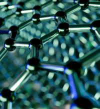
Nanotechnology Revolutionising technology
industry
APICAM2021 PAGE 8 MAMAS 2020 PAGE 10 LMT2021 PAGE 15 Women In The Industry PAGE 22 University Spotlight PAGE 36 Online Short Courses PAGE 56
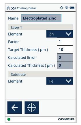
Rede ning Coating Thickness Measurement
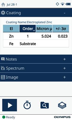
Measuring the thickness of galvanized or electroplated coatings on any substrate is as easy as 1 – 2 – 3

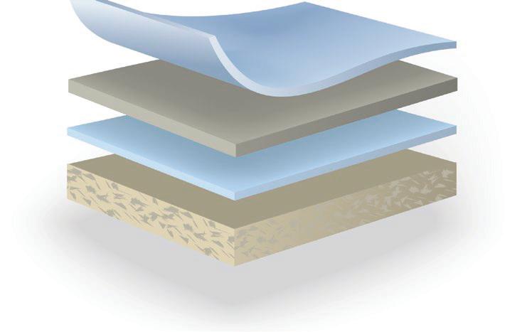
Choose a galvanized, electroplated, or coated sample of any substrate: metal, plastic, glass or even wood
Get right to work with our factory coating method, or customize for a speci c application with the optional single-point calibration.
Vanta analyzers quickly and accurately measure up to three layers of coatings at the micron level.
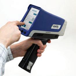

For more information contact Olympus Australia/New Zealand:
1300 13 2 99

22 20 M crons Ti 23 20 Microns V 24 25 M crons Cr 25 25 Microns Mn 26 25 Microns Fe 27 30 Microns Co 28 30 Microns Ni 29 30 M crons Cu 30 30 Microns Zn 40 35 M crons Zr 41 40 Microns Nb 42 40 M crons Mo 45 10 M crons Re 46 40 Microns Pd 47 45 M crons Ag 48 30 Microns Cd 50 45 M crons Sn 51 45 Microns Sb 72 10 Microns Hf 73 10 M crons Ta 74 10 Microns W 79 10 M crons Au 82 20 Microns Pb 83 20 M crons Bi Common Elements & Maximum Coating Thickness. Most common in corrosion-resistant coatings Substrate Measure up to three coating layers at the micron level Large,
LCD
screen
click control
color
touch
with swipe and
( Austr alia):
2 (N e w Z eala nd ): 0 50 8 6 59 6 787 IB Di nf o @ Olym pus. co m .a u ww w.olympus-ims.com/Vanta Olympus is a registered trademark, and Vanta is a trademark of Olympus Corporation
From the President
The Impact of COVID-19
Australians are moving through an important point in history that will impact our lives for some years to come. Within a reasonably short period of time, we have seen our daily commute replaced with working from home arrangements and home-schooling, or being subject to complete workplace shut downs. For those of us who have continued working through the lockdown, we face the new challenge of social distancing in workplaces. This has necessitated a rethink of the way in which we organise our workflow, production and interactions with our colleagues.
Welcome to the June 2020 edition of Materials Australia magazine, and my first President’s Report.
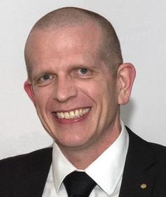
I took on the role of Materials Australia National President in May 2020. As such, I thought I would start by introducing myself. A Physical Metallurgist, I completed a Bachelor of Science (Hons.1), PhD and Doctor of Engineering at the University of Queensland. Since then, my professional experience has spanned roles in research, industry, and academia.
I am a registered Chartered Engineer and Fellow of Engineers Australia, as well as a registered Chartered Engineer and Scientist in the United Kingdom through the Institute of Materials, Minerals and Mining. I am also an elected Fellow of the Academy of Technological Sciences and Engineering.
I advocate for Australian manufacturing, as a member of the Victorian Skills Commissioner’s Industry Advisory Group, and deputy chair of the Victorian Defence Alliances Submarines Committee. I strongly believe in the value of business-to-business research and development initiatives as a path to technology commercialisation in advanced manufacturing industries.
As a Senior Technical Specialist with AWBell in Melbourne, I lead the company’s long-term research strategy and advanced manufacturing technology development associated with ferrous and non-ferrous metal casting, as well as being the Level III for non-destructive testing. I am also working on the development of a new training program for the VET sector in Precision Investment Castings, supported by the Department of Education and Training in Victoria.
We have had to shore up our supply chains and evaluate risk differently to ensure we have the materials and resources we need to operate. We have all become experts at meeting via Zoom and it is encouraging to see technical presentations attract larger audiences when online than they might have if presented in person.
What has become
The Opportunities Ahead
What has become clear from the events that have unfolded during the first half of 2020 are the fantastic opportunities available to the materials and manufacturing communities in the coming months and years.
We need to plan for an altered economy where the importance of sovereign capability and self-sufficiency begin to take on new importance. I recently read the results of a survey of nearly 30,000 people, which showed that in the current economic climate, 97% of respondents believed that Australia should become less reliant on imports.
I have stated for many years that people are proud of the products made by their countrymen and will support local industries where possible. I also believe that this message will not fall by the wayside when the current situation subsides. Together, with support from our energy sector, we can build a strong, modernised manufacturing industry utilising advanced materials and technologies that position Australia for the future.
I also have to note that some of the Materials Australia events originally planned for 2020 have been deferred to later dates. We are going to have a very busy 2021, with APICAM 2021 and LMT 2021 both already scheduled for July, and the CAMS meeting (which was originally scheduled for 2020), now planned for December 2021.
I would like to draw your attention to the fact that Materials Australia facilitated five different online meetings in June, including three webinars and two panel discussions. There is a great opportunity to continue these networking opportunities online and take part in professional development. Our corporate sponsors deserve special acknowledgement of their support for Materials Australia and their resilience during this time. I look forward to showcasing more of their capabilities, their successes, and their special projects in future issues of the Materials Australia magazine.
Finally, I would like to acknowledge the fantastic job Paul Plater (outgoing President of Materials Australia) and Dr Robert Acres (outgoing Vice President of Materials Australia) have done during their time in the roles. They have left the organisation in a very good position. I hope that, together with the National Executive Committee and the National Council, I can work to continue to deliver outstanding services to our members.
2020 continues to be a challenging year. I would like to wish you, your family and colleagues the best of health and to stay safe. Materials Australia looks forward to seeing you all at our online events, and then in person, once the pandemic has safely passed.
Best Regards
Roger Lumley, National President
WW W.M ATERIALSAUSTRALI A COM AU BACK TO CONTENTS 3 | JUNE 2020 MATERIALS AUSTRALIA
clear from the events that have unfolded during the first half of 2020 are the fantastic opportunities available to the materials and manufacturing communities.

CONTENTS 28 MANAGING EDITOR Gloss Creative Media Pty Ltd EDITORIAL COMMITTEE Prof. Ma Qian RMIT University David Hart Tanya Smith MATERIALS AUSTRALIA ADVERTISING & DESIGN MANAGER Gloss Creative Media Pty Ltd Rod Kelloway (02) 8539 7893 PUBLISHER Materials Australia Technical articles are reviewed on the Editor’s behalf PUBLISHED BY Institute of Materials Engineering Australasia Ltd. Trading as Materials Australia ACN: 004 249 183 ABN: 40 004 249 183 Cover Image From feature article on page 44. Letters to the editor; info@ glosscreativemedia.com.au Nanotechnology Revolutionising technology and industry at an atomic scale VOLUME 53 NO 2 JUNE 2020 ISSN 1037-7107 September 2014 Focus on Education and Training. Targeting: universities, high school students and vocational training. Advertising Deadline: Friday 5th September December 2014 Content Deadline: Friday 21st November Advertising Deadline: Friday 28th November Materials Australia has planned the following featu es for 2014, designed to highlight di fe ent disciplines and sectors Our aim is to publish elevant, inte esting and cur magazine for those involved in all aspects of Materials. and your business is active in one of these a eas, then you will want to be involved. W fer your company the opportunity to p omote y Materials Australia also encourages members to contribute to our magazine and we will consider all editorial contributions. For further details, please contact: Gloss Creative Media Pty Ltd T +61 2 8539 7893 email: magazine@materialsaustralia.com.au www.glosscreativemedia.com.au September 2014 Friday 29th August Advertising Deadline: Friday 5th September December 2014 Friday 21st November Advertising Deadline: Friday 28th November Materials Australia has planned the following featu es for 2014, designed to highlight di fe ent disciplines and sectors of the Materials Community Our aim is to publish a elevant, inte esting and cur magazine for those involved in all aspects of Materials. and your business is active in one of these a eas, then you will want to be involved. fer your company the opportunity to p your business di ectly to decision makers in the contribute to our magazine and we will consider +61 email: magazine@materialsaustralia.com.au www.glosscreativemedia.com.au APICAM2021 PAGE MAMAS 2020 LMT2021 PAGE 15 Women In The Industry University Spotlight Online Short Courses PAGE 56 Reports From the President 3 Contents 4 Materials Australia - Corporate Sponsors | Advertisers 6 Materials Australia News APCIAM2021: A Truly International Conference 8 RMIT University’s Centre for Additive Manufacturing 8 MAMAS 2020 10 WA Branch Report 12 NSW Branch Report 12 Metallurgy for Non-Metallurgists - WEBINAR 12 MAMAS | Materials Australia Golf Day - 21 Oct 2020 13 Professor David StJohn Wins the 14 2020 Bruce Chalmers Award Light Metals Technology (LMT) Conference 15 Things I Wish I Knew When I Was a Science 16 and Engineering Student CMatP Profile: Dr Andrew Ang 18 Our Certified Materials Professionals (CMatPs) 20 Why You Should Become a CMatP 21 Women in the Industry 22 Professor Nikki Stanford 10 14 MAMAS | 2020 4 | JUNE 2020 WW W.M ATERIALSAUSTRALI A COM AU
This magazine is the official journal of Materials Australia and is distributed to members and interested parties throughout Australia and internationally. Materials Australia welcomes editorial contributions from interested parties, however it does not accept responsibility for the content of those contributions, and the views contained therein are not necessarily those of Materials Australia. Materials Australia does not accept responsibility for any claims made by advertisers. All communication should be directed to Materials Australia. Materials Australia National Office PO Box 19 Parkville Victoria 3052 Australia T: +61 3 9326 7266 E: imea@materialsaustralia.com.au W: www.materialsaustralia.com.au NATIONAL PRESIDENT Paul Plater CONTENTS 36 44 Industry News When One Door Opens: Monash Student Develops 24 3D Printed Key to Prevent COVID-19 Spread Ultrafast Probing Reveals Intricate Dynamics 25 of Quantum Coherence The Power of Sound Waves Making Noise 26 with New Research Synthetic Material Could Help Heal Injured 27 Tendons and Ligaments Australian Innovation Leads to Sustainable 28 Alternative for Architectural Hardwoods Bridging the Gap to the Synchrotron 30 Time Resolved MicroCT in the Lab is Now a Reality 32 CAMS2021 33 Davenport PETPlus IV for measuring 34 Intrinsic Viscosity of PET Polymer Next Generation Phenom XL G2 Desktop SEM 35 Brings Advanced Automation to the Forefront University Spotlight: University of Western Australia 36 Breaking News 38 Feature Nonotechnology 44 Materials Australia - Short Courses 56 www.materialsaustralia.com.au/training/online-training 30 WW W.M ATERIALSAUSTRALI A COM AU 5 | JUNE 2020




















MATERIALS AUSTRALIA 6 | JUNE 2020 BACK TO CONTENTS WW W.M ATERIALSAUSTRALI A COM AU Corporate Premium Plus
Premium
Corporate




















WW W.M ATERIALSAUSTRALI A COM AU 7 | JUNE 2020 MATERIALS AUSTRALIA Corporate Advertisers - June 2020 APICAM2021 MAMAS | 2020 MELBOURNE AUSTRALIA MELBOURNE AUSTRALIA MELBOURNE AUSTRALIA GLOBAL STEEL HEAT TREATMENT Advancing Materials and Manufacturing Call: (03) 9540 5100 Dynamic & Fatigue testing system Ergonomic, Versatile, High Performance Testing System www.bestech.com.au Testing wide range of materials: • Advanced/ Biomedical • Manufacturing Assemblies • Dental Implants TMF, LCF, Fracture Mechanics, HCF, High-strain rate & Component testing ForallyourMetallographicRequirements www.kemet.com.au Kemet Precision Lapping Polishing Cleaning Materialography
APCIAM2021: A Truly International Conference
APICAM was created to provide an opportunity for industry professionals and thoughtleaders to come together, share knowledge and engage in the type of networking that is vital to furthering the additive manufacturing industry.
APICAM2019 was a resounding success, with over 300 delegates and speakers attending over the three days of the conference. The delegates came from 15 different countries, ensuring this was a truly international conference. APICAM2021 is sure to be just as successful.
Attendees heard from some of the leading minds in the industry, who presented highly informative and engaging presentations on pressing issues, as well as the ways in which innovations can navigate challenges. Important areas such as 3D printing and additive manufacturing in the automotive, biomedical, defence and aerospace industries were covered by experts from each respective field.
The 2019 keynote presentations included: Production Level Additive Manufacturing by Yathiraj Kasal (from GE); I AM SIEMENS – Industrialised Additive Manufacturing by Siemens by Ingomar Kelbassa (from Siemens); Recent Developments in Additive Manufacturing in Europe by Professor Christoph Leyens (from the Technische Universität); 3D Printed Orthopaedic Implants in China by Professor Huiping Tang (from the Northwest Institute for Nonferrous Metal Research); Polymers for Powder Bed Fusion by Professor David L. Bourell (from the University of Texas); and Structure Evolution Across Build Layers in EB Additive Nickel Alloys by Professor Tresa Pollock (from the University of California). The line-up of speakers for APICAM2021 is shaping up to be just as engaging.
With tickets to APICAM2019 selling out in record time, be sure to ‘save the date’ for APICAM2021: 7-9 July 2021 at RMIT University in Melbourne.
RMIT University’s Centre for Additive Manufacturing
APICAM2021 will be held at RMIT University in Melbourne, which is home to the Centre for Additive Manufacturing.

The objective of the Centre for Additive Manufacturing is to increase the competitiveness of global supply chains for industry partners, through innovation in additive manufacturing technologies, materials science, digital design and laser technologies.
The Centre provides integrated solutions to the aerospace, biomedical, defence, automotive, and power generation industries. Their fundamental and applied research is driven by market requirements and focuses on design, materials and manufacturing and system development.
The Centre’s research is focused on additive manufacturing of components in advanced materials such as high performance metals,
plastics and composites. By transitioning from rapid-prototyping to full-scale manufacturing of customised functional products and parts, directly from design, their researchers are able to remove the need for tooling.
World-Leading Research
Just some of the research projects currently underway at the Centre are outlined below. A novel approach to the design and fabrication of biomimetic and biocompatible Ti-Ta for bone implants by additive manufacturing
This multidisciplinary ARC-supported research project aims to combine structural and materials engineering, additive manufacturing and tissue engineering to develop biomimetic bone-like scaffolds with superior structural, mechanical and biological compatibility as bone substitutes.
CONFERENCE CO- CHAIRS
Jian-Feng Nie is a professor at Monash University. His current research interests cover physical metallurgy of magnesium and aluminium alloys, applications of scanning transmission electron microscopy in materials characterisation, and processing-microstructure-property relationships in metallic alloys.
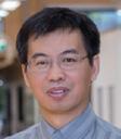

Dr Ma Qian is Distinguished Professor of Advanced Manufacturing and Materials at RMIT University. Professor Qian joined RMIT from the University of Queensland in 2013, where he was the Reader in Materials Engineering, School of Mechanical and Mining Engineering. His areas of research include: metal 3D printing or additive manufacturing, powder metallurgy of light metals and alloys, solidification processing, metallic biomaterials and biomimetic surface designs, micro-nano-architectured materials.
Additivemanufacturingproductivitygains forindustry
The Victorian Government’s grant for Manufacturing Productivity Networks aims to improve the productivity and competitiveness of Victorian manufacturing businesses. Together with industry partners, the Centre’s researchers are examining several components for additive manufacture and demonstrating the design and fabrication possibilities in polymers and selected metals together with their cost benefit analysis.
Repairtechnologiesforcurrentandnext generationaircraftsystems
The principal aim of this project is to develop and certify safe, timely and costeffective repair technologies for current and next generation military aircraft, particularly, direct metal deposition technologies.
MATERIALS AUSTRALIA
8 | JUNE 2020 BACK TO CONTENTS WW W.M ATERIALSAUSTRALI A COM AU
APICAM2021
The 3rd Asia-Pacific International Conference on Additive Manufacturing (APICAM) is the not-to-be-missed industry conference of 2021. APICAM was created to provide an opportunity for industry professionals and thinkers to come together, share knowledge and engage in the type of networking that is vital to the furthering of the additive manufacturing industry.
Some of the leading minds in the industry will give presentations on pressing issues and the ways in which innovations can navigate challenges. Important areas such as 3D printing and additive manufacturing in the automotive, biomedical, defence and aerospace industries will be covered by experts from each respective field.
The event is being curated by Materials Australia, the peak Australian materials technology body, which has drawn on its considerable pull in the industry to create a world-class event that is a must-attend for anyone involved in the additive materials industry.
The main features of APICAM2021 will include presentations by experts, as well as workshops, that will help attendees sharpen their skills, enabling them to pass on knowledge to other industry professionals. The event has been designed to allow for ample networking time so that important knowledge-transfer can take place and partnerships can be created that will enrich the industry.
The purpose of this conference is to provide a focused forum for the presentation of advanced research and improved understanding of various aspects of additive manufacturing. This conference will include lectures from invited internationally distinguished researchers, contributed presentations and posters. Contributions will be encouraged in the following areas of interest:
Additive Manufacturing of Metals

Additive Manufacturing of Polymers
Additive Manufacturing of Concretes
Advanced Characterisation Techniques and Feedstocks
Computational Modelling of Thermal Processes for Metallic Parts
Part Design for Additive Manufacturing
Failure Mechanisms and Analysis
Mechanical Properties of Additively
Manufactured Materials
New Frontiers in Additive Manufacturing
Process Parameter and Defect Control
Enquiries: Tanya Smith | Materials Australia +61 3 9326 7266 | imea@materialsaustralia.com.au www.apicam2021.com.au
Process-Microstructure-Property Relationships
Testing and Qualification in Additive Manufacturing
WWW.MATERIALSAUSTRALIA COM AU BACK TO CONTENTS JUNE 2020 | 9
7 - 9 July 2021
RMIT University, Melbourne
Asia-Pacific International Conference on Additive Manufacturing
0 2 0
BUNBURY – 22 OCTOBER 2020

THE DOLPHIN DISCOVERY CENTRE

LOT 556, KOOMBANA DRIVE, BUNBURY
7:00AM – 5:00PM (Including Site Visit to Geographe)









M ATERIALS A ND M AINTENANCE A DVANCEMENTS IN THE S OUTH WEST 2
PLATINUM SPONSOR GOLD SPONSOR SUPPORTER 10 | JUNE 2020 BACK TO CONTENTS WW W.M ATERIALSAUSTRALI A COM A
SEMINAR SERIES BRONZE SPONSORS
MAMAS | 2020
TECHNICAL SEMINAR DETAILS –THURSDAY 22 OCTOBER 2020
Following the successful inaugural event in 2018, the Western Australia Branch of Materials Australia (the Materials Society of Engineers Australia) and the AINDT are proud to be hosting this event for the second time in Bunbury after many delegates indicated that they would like to attend future events in the region.

This regional technical seminar represents recent and relevant advancements in materials and maintenance practices in various industries active in the South West of Western Australia.

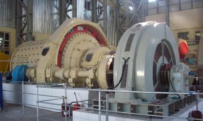
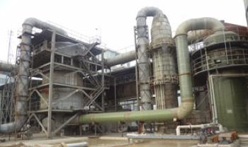
The successful application of materials and maintenance programs to plant and equipment is critical to the optimisation of an asset life cycle. The life extension of mining, processing and infrastructure assets is critical in the current industry environment. Within this, the performance of materials during more and more extended maintenance periods is a major component. Maintenance based technologies continue to evolve and their interplay with advanced materials will be presented and discussed. This is a great opportunity to learn from real case studies from industry and to hear from a number of West Australian and local experts in their field at this exclusive event.
KEYNOTE SPEAKER DR PETER FARINHA PRINCIPAL, EXTRIN CORROSION CONSULTANTS
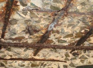
As a specialist corrosion engineer, holding both a Masters and PhD in Corrosion Science & Engineering, Dr. Peter Farinha has been involved in identification and problem solving of corrosion related issues in steel corrosion and reinforced concrete, including inspection, identification, failure analysis, materials selections, coatings, specification and repair methodology for over 30 years. He is a specialist in microbiological corrosion, heavily involved in ALWC and he has published broadly.
GOLF DAY – WEDNESDAY 21 OCTOBER MERCURE SANCTUARY GOLF RESORT
The seminar will be preceded by a Golf Day at the Mercure Sanctuary Golf Resort. Tee off will be at 1:00pm, Ambrose rules will apply. You can register as an individual (and be allocated onto a team) or as a team of four.
The costs will be: $80 per person or $320 for team of four. This cost includes nine holes, a Golf Cart shared between two people and a BBQ Dinner at the venue.
Please contact Colm Kinsella on Colm.Kinsella@Olympus.com.au or register yourself or your team at Trybooking
To stay overnight at the venue contact Mercure Sanctuary Resort on (08) 9725 2777.
REGIONAL TECHNICAL SEMINAR SERIES
SPONSORSHIP
Various opportunities are available for sponsorship with three levels: Bronze $500, Silver $1200 and Gold $1750.
Please contact:
PAUL HOWARD on 0407 711 008 or paulh@gerard-daniels.com

PAUL HUGGETT on 0411 868 289 or paul.huggett@applusrtd.com to discuss.
SITE VISIT –GEOGRAPHE
57 CRAIGIE STREET, DAVENPORT
The seminar will be followed by a Plant Visit to the Geographe facilities in Bunbury. Delegates will be transported by bus from the Dolphin Discovery Centre to the Geographe facilities at 2:30pm returning at 4pm. Geographe has recently commissioned three new manufacturing cells and facilities that they will be able to demonstrate on the day.
BRONZE SPONSORS PLATINUM SPONSOR GOLD SPONSOR SUPPORTER
WW W.M ATERIALSAUSTRALI A COM AU BACK TO CONTENTS 11 | JUNE 2020
WA Branch Report
Source: Steve Algie
Along with most of the business world, the Western Australia Branch Council has quickly adapted to the shift to Zoom online meetings. We held our April and May 2020 meetings using this platform, and found the virtual meeting format very effective.
The only problem was that the worldwide shortage of webcams meant that a couple of Councillors had to make do with limited technology. This problem served as a reminder of the supply challenges that will be confronting many businesses in our industry over coming months. We recognise that these are difficult times,
NSW Branch Report
and we are doing what we can to keep the supply of technical information flowing to members.
We have rescheduled our planned one-day seminar in Bunbury to 22 October 2020, in the expectation that most restrictions on gatherings will have been lifted. We have had great responses from speakers and sponsors, and all have agreed to continue their support.
The main disruption to our technical program has been the inability to proceed with site visits. We had three site visits planned this year and it seems unlikely that any of these will proceed. To compensate, we have sought to substitute
the visits with technical presentations. We may be able to return to in-person meetings, with appropriate social distancing (and no finger food!). However, our immediate plan is focused on online meetings using Zoom. Registering for Zoom meetings is quite straightforward: register using the TryBooking app, after which we will email you a link to the meeting.
Our first Zoom technical meeting was held on Monday 8 June 2020, preceded by our Branch AGM. The topic was ‘Materials characterisation: an integral part of advanced manufacturing and 3D printing’, presented by Dr Zakaria Quadir of Curtin University.
Source: Associate Prof Sophie Primig, University of New South Wales
Given the current climate, and various social distancing measures that are in place, the New South Wales (NSW) Branch has moved its events to an online teleconferencing format. We have several exciting events planned over the next couple of months, and encourage all members to attend.
On Tuesday 9 June 2020, the NSW Branch and the Australian Ceramics Society held a free is holding a free Careers Path Seminar via Zoom. Our five speakers described their career paths, including how they got to where they are, what they love about their job, and what elements of their careers have been more difficult. This was followed. by a Q&A session.
Speakers included Professor Vanessa Peterson (Senior Principal Research and Neutron Scientist, ANSTO), Dr Alan Xu (Materials Engineer, ANSTO), Dr Rui Hoo (Research Development Manager for Strategic Initiatives, University of Sydney), Dr Sarah Grundy (Education Focussed Academic, UNW) and Dr Kenny Cheung (Materials Engineer, Pallion).
In August, we plan to hold a webinar on the topic of Metallurgy for Non Metallurgists. The presenters include Professor Madeleine du Toit (University of Wollongong), Professor Huijun Li (University of Wollongong), and Dr Nima Haghdadi (UNSW).
Metals and alloys are used in the largest variety of applications of all engineering materials. As such, it is essential for those
involved in manufacturing, engineering and construction to have an understanding of what metals (ferrous and non-ferrous) are, how they behave, and why they behave differently to ceramics, glass, and plastics.
It is also important to understand how metals and alloys can be made stronger, how they can be shaped by casting, forging, forming, and how these processes, along with heat treatment, can alter properties. This course provides important basic knowledge to those who are not metallurgists.
To register for these events, visit: https:// www.materialsaustralia.com.au/events/ branch-events/nsw
Topics may include:
Introduction to Metals & Alloys

Solidification of Metals
Metal Forming
Mechanical Properties
Strengthening Mechanisms
Heat Treatment
Strengthening Steels & Cast Iron
Materials Characterization & Selection Failure Analysis
MATERIALS AUSTRALIA
Register Now Metallurgy
Non-Metallurgists WEBINAR - Training Workshop 12-14 August 2020 | 12.30 pm - 5.00 pm
for
12 | JUNE 2020 BACK TO CONTENTS WWW.MATERIALSAUSTRALIA COM AU
AINDT & MATERIALS AUSTRALIA

GOLF DAY 2020

Date: Wednesday 21st October, 2020
Course: Mercure Sanctuary Golf Resort

Address: Lot 100 Old Coast Rd, Pelican Point WA, 6230
Tee Time: 1:00 pm shotgun
Golf Format: Ambrose Format


Teams: You can register as an individual (and be allocated onto a team) or as a team of four.
Opportunity for short welcoming and closing presentation at the start and end of the event.
Presentation of awards for the competitions.
Logo on all promotional material.
Cost: The costs will be:
• $80 per person or
• $320 for team of four.
This cost includes 9 holes and a Golf Cart shared between 2 people.
Food: BBQ Dinner will be provided at the venue.
Competitions include...
Longest Drive
Nearest to the Pin Best Overall team score
To register for a team or for further enquiries around the event or sponsorship, please contact Colm Kinsella on Colm.Kinsella@olympus.com.au
To stay overnight at the venue, contact Mercure Sanctuary Resort on (08) 9725 2777.
FOR SPONSORSHIP Have your brand recognised! Package Benefit Major $500 Supporting $200
CALLING
Event naming rights. Recognition on the day as well as in all future publications of the event.
Materials and Maintenance Advancements in the South West Seminar will follow on 22nd October from 7:00 am to 5:00 pm at The Dolphin Discovery Centre, Bunbury (including Site Visit to Geographe).
TAKEN
Professor David StJohn Wins the 2020 Bruce Chalmers Award
Source: Sally Wood
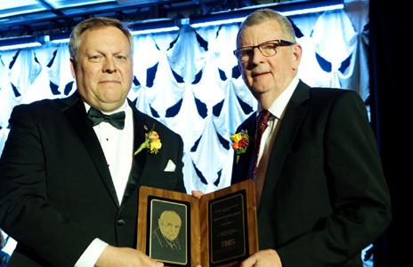
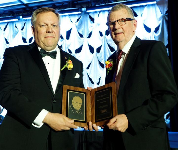
Emeritus Professor David StJohn from the University of Queensland has been awarded the 2020 Bruce Chalmers Award by The Minerals, Metals and Materials Society (TMS).
The Bruce Chalmers Award recognises an individual who has made outstanding contributions to the science or technology of materials processing, and includes a life-time membership to TMS.
The award honours Bruce Chalmers, a professor of metallurgy and former master of John Winthrop House at Harvard University. Chalmers was a senior researcher in physics and atomic energy during and after World War II in Britain. He joined the Harvard faculty as Gordon McKay Professor of Metallurgy in 1953. Chalmers served as master of Winthrop House, an undergraduate residence, from 1964 to 1975. He retired in 1977 after 24 years as a professor in Harvard’s division of engineering and applied sciences. Harvard University called him ‘an authority in the field of metallurgy’.
Professor StJohn received the award for his outstanding contributions to the solidification science of nucleation during grain refinement, and the materials processing of aluminum, magnesium and titanium alloys of technological importance.
According to Professor StJohn, “It is a great honour to have been chosen for this award. Bruce Chalmers’ work on constitutional supercooling was an important concept studied during my PhD, and it has been a key element of my, and my colleagues’, research on grain refinement and nucleation ever since.”
“Of the many awards that TMS offers, this one is closest to my research interests, and I thank TMS for recognising the contribution that Bruce Chalmers made to metallurgy and, in particular, the field of solidification. Receiving this Award was made possible by the contributions of my students, research fellows, and collaborators, and therefore this award belongs to all of us,” said Professor StJohn. Professor StJohn’s research is focused on
solidification technology, with particular interest in grain refinement and the formation of defects in castings of aluminium, magnesium and titanium alloys. He has over 300 publications in journals and conference proceedings, and was awarded the John Campbell Medal in 2014, the Materials Australia Silver Medal in 2011, the American Society of Metals Henry Marion Howe Medal in 2006, and the Magnesium Technology Award by TMS in 2003.
Professor StJohn is a graduate of the University of Queensland (UQ) with a Bachelor of Science (Hons) and PhD in Physical Metallurgy. He has held appointments in Canada, RMIT University and CRA-Advanced Technical Development in Perth, as well as his long-held association with UQ.
From 1994 to 2008, he was with the CAST Cooperative Research Centre, becoming CEO from August 2002 until 2008. He led the successful bid for the Defence Materials Technology Centre (DMTC) in 2008, and initiated the Centre
for Advanced Materials Processing and Manufacturing (AMPAM) at UQ in 2009. He also successfully led an application to the Queensland State Government to fund a new building to house AMPAM, which led to a further application to the Australian Federal Government for additional funding to construct the Advanced Engineering Building (AEB). He was then Chair of the Project Control Group for the construction of the AEB, which was completed in 2013.
Professor St John has made a significant contribution to developing research partnerships with industry and obtaining financial support for research and education facilities (totalling more than $300 million). Since 2003, this has included $130 million for the new Advanced Engineering Building at UQ, $70 million for industry-research partnerships such as the CAST CRC and the DMTC, and over $2 million for competitive research funding including several ARC grants. Current industry partners include Cook Medical, Bluescope Steel, Nihon Superior, Magontec and Baosteel.
MATERIALS AUSTRALIA
14 | JUNE 2020 BACK TO CONTENTS WW W.M ATERIALSAUSTRALI A COM AU
L to R: TMS 2020 President James Foley and Professor David StJohn.


2014
Themes
Things I Wish I Knew When I Was a Science and Engineering Student
Proceeding through university in a science or engineering discipline is a challenging process in many ways. Knowing what to expect in the approaching years is incredibly useful, and gaining this insight from fellow students will help you to remain prepared for the upcoming stages in your studies. Here are five tips and perceptions regarding the undergraduate science and engineering study path that I wish I had been aware of when I was a student.
1. Notetaking Tips
As a first-year student, newly enrolled at university, it can be challenging to know which information delivered to you by your lecturer is important to remember. This can make notetaking a rather problematic activity, particularly if the content is delivered quickly. However, there are some ways to make the most of notetaking exercises.
Listen out for obvious cues from your teacher. They will often advise you which information is particularly important for you to know by saying things such as “this is very important for you to know” and “it would be useful for you to know how to solve this type of problem before you sit the exam”. Make the most of these hints as they have been given out for a good reason.
When highlighting sections of textbooks or notes, try to select only crucial pieces of information so that you can easily find that section on the page when you revisit it later.

Avoid copying down large amounts of information such as tables of data, large chunks of text and information that is present on lecture slides or notes. This information will typically be available for you to look back on later. Instead, try to prioritise added information or facts that the lecturer may bring up in addition to the information in front of you. These types of additional information may not be accessible after the lecture has finished. Remembering these small, useful, bite-sized facts leads nicely onto our second tip.
2. Remember the Little Things
Becoming an excellent materials scientist is not about learning a huge amount of information about a single topic from day one. On the contrary, it is more useful to have a good general understanding about the properties of many materials, and their interactions with their surroundings, as possible. Also important are physical testing methods, manufacturing processes and chemical or microstructural analysis techniques. Even if you do not remember every detail, an overview is important, keep them in the back of your mind. Harbouring as much general knowledge as possible will allow you to think outside the box, and one day you will be able to use that knowledge to tackle a problem that the ‘standard’ set of tools cannot solve.
3. Avoiding Misinformation

We are living in the age of information, which leads to unprecedented benefits in regards to our ability to search ‘online’ for anything.
However, therein lies the problem: we can search for anything, but that does not necessarily mean that the facts are true. While reports of ‘fake news’ have been published by all forms of media for an incredibly long time, there has certainly been an increase in the number of misinformed articles, along with the presence of social media. It is extremely
difficult, if at all in some cases, to police the posting of false information through our various media platforms. Coupled with this, we have an extremely active online social presence, in which this false information can spread like wildfire. Like anything that is posted online, the initiation of false information is something that cannot be wiped from existence. Differentiating fact from fiction can come down to using common sense; I have seen media articles publishing stories slamming the renewable energy field for “using up all Earth’s wind, sun or waves”. Other articles can be more difficult to determine their truth. The best way to do this is to get your information from credible sources. Try to find the original research article if possible, or ensure that wherever you get your information from is getting their information from a credible source. Such sources include peerreviewed journal articles in which the research needs to be approved by several world experts in the area of the research, or government agencies. However, even this does not always ensure that the information is truthful. A group of graduate students from MIT University wrote an algorithm in 2005 which creates a computer-related research topic and automatically produces an entire research paper (including graphs, figures and
MATERIALS AUSTRALIA
16 | JUNE 2020 BACK TO CONTENTS WW W.M ATERIALSAUSTRALI A COM AU
Source: Peter Richardson – NSW Branch Committee
references) from it, with a single click of a button. They submitted these papers to several journals and found that some were accepted through the peer review process for publication. This process of submitting fake papers has since been used to test individual journals’ peer review processes and ensure the quality of research published by our scientific community. The abstract of one of these randomly generated papers is shown below.
4. Reading a Research Paper

Learning how to read a research paper on any topic can be a daunting task, and materials science papers are no different. However, just remember that learning to read these documents is like learning
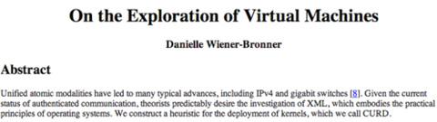
to ride a bike: frustrating, tiresome, time consuming, but ultimately exciting, rewarding and even enjoyable! It is not uncommon for new students in the field to take hours or even days to read a single paper from start to finish. There are two main reasons for this. Firstly, if you can read any single sentence in your first paper without stumbling across a word, phrase, abbreviation, symbol or acronym you don’t understand, you are doing well. The scientific community is rife with technical jargon, which plays a very important role. It has been specifically developed within the field to provide an extremely precise description of certain phenomena, which ultimately helps to keep the reporting of new observations as concise as possible. You will spend a huge amount of time looking up new terms, which will then be added to your own vocabulary. This will not only build your understanding of the work presented to you, but also improve your own technical writing capability down the track. Secondly, due to your newfound enthusiasm for research, it is likely that you will try to read the paper from start to finish, taking in every word along the way. While this makes for an excellent learning experience, it is a long and laborious way to read a paper. As you read more and more papers in your field, you will become familiar with the typical jargon, experimental methods, ways in which the results are displayed and order in which the information is presented. With this experience comes the ability to quickly flick to the part which gives you the information you are specifically after, and greatly increases the rate at which you can digest new works.
5. Why Materials Research is the Way to Go
So, you’ve decided to become a scientist. Great choice! You obviously have a keen interest in finding out how the world around you works. Materials science is a fascinating area of science that binds many different topics together such as physics, chemistry, engineering, biology, to name a few. Not only does materials science combine these areas together, it also acts across an enormous scale range. You could be developing new steels or concrete materials for the construction of huge skyscrapers, tunnels and bridges. Alternatively, you could be looking at individual atoms within your material sample through a transmission electron microscope, or designing nano-electronic devices which exhibit single photon emission for quantum communication systems. In all cases, materials science is an exciting translational science, taking new ideas from theoretical conception all the way to engineering implementation. You will play an important role in this translation. Your work could be computational, running simulations to predict which materials have the best properties for a unique application. On the other hand, you could be creating new materials in the laboratory, testing their performance using highly technical equipment, or developing new processes to make those materials in a largescale or economically feasible way. Whatever your role, you will make an exciting and important contribution to the advancement of our scientific knowledge and the development of new technologies.
MATERIALS AUSTRALIA WW W.M ATERIALSAUSTRALI A COM AU BACK TO CONTENTS 17 | JUNE 2020
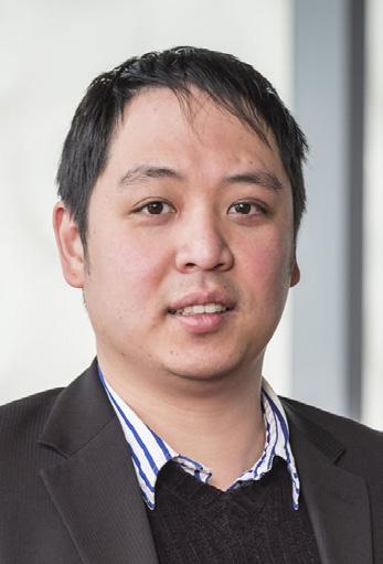
CMatP Profile: Dr Andrew Ang PhD, CMatP, MIEAus
engineering and, better still, ST Land System offered me a job at the end of my internship.
Who or what has influenced you most professionally?
This is a tough question because I have been lucky to work with so many wonderful people. However, two people really stand out. The first person is Associate Professor Philip Cheang (aka Doc Phil), who sadly passed away a couple of years ago. Doc Phil taught me about biomaterials and we worked on cold spray biocoatings. Even though, at the time, he was the Head of School at SIM University, Doc Phil always had time to have coffee; his enthusiasm and passion for research excellence was contagious.
Where do you work?
Describe your job.
I am a Senior Research Engineer at Swinburne University of Technology. In this role, I lead a diverse research team focused on the topics of surface engineering and materials science, with a particular focus on the subject of thermal spray coatings and thin films.
What inspired you to choose a career in materials science and engineering?
Prior to coming to Australia, I completed my undergraduate degree at the National University of Singapore. It was during the third year of my course that I had an opportunity to complete an internship at ST Land System (then called Singapore Technology Kinetics)—a defence engineering contractor.
Whilst undertaking this internship, I came to understand the importance of engineering materials. I was involved in some of the most impressive projects that an undergraduate could ever imagine — from looking at thermite reactions (which generate huge amounts of heat), to the development of new materials for ballistic protection (including their destruction). It is fair to say the experience ‘ignited’ my interest in materials science and
The second person is my PhD supervisor, and now colleague, Professor Christopher Berndt, who has tirelessly mentored many young budding engineers in the field of thermal spray. For those that know Chris well, he embodies the most generous spirit and has the tenacity to lead pioneering research into coatings and materials.
What has been the most challenging project you’ve worked on to date and why?
I am currently one of the chief investigators at the ARC Training Centre: Surface Engineering for Advanced Materials (SEAM), which consists of 12 industry partners, two national labs
(ANSTO and CSIRO), and three universities. Indeed, a large team of people working together.
There are multi-projects within SEAM involving various stakeholders, many of which are working to address the critical manufacturing needs of an ever-changing global and Australian economy. The greatest challenge is to fulfil the industry research objectives, while simultaneously upskilling or re-skilling the workforce so that it is able to work with the new technology. Such an endeavour will require significant time and effort, but I believe the research impact will be wide reaching and worthwhile.
What does being a CMatP mean to you?
Working in the field of material science and engineering, I believe it is a privilege to be recognised by my peers as a CMatP. Professionally, it has given me the opportunity to be involved in standards committees, and widen my professional network with others.
What gives you the most satisfaction at work?
Apart from working with my team of awesome researchers, I get most satisfaction from our applied research that has solved challenging engineering problems for our industry partners.
Thermal sprayed coatings, developed in partnership with our labs, are now found in many essential applications in Australia,
MATERIALS AUSTRALIA
18 | JUNE 2020 BACK TO CONTENTS WW W.M ATERIALSAUSTRALI A COM AU
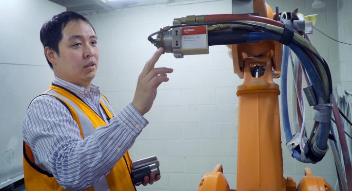
Andrew can deposit various types of coatings via plasma spraying (20,000°C plasma flame jet). Follow his research @ASMcoatings on Twitter.
from better wear resistant coatings for power generation (such as power stations) and new anti-corrosion coatings for naval vessels, right through to thermal barrier coatings for automotive components. There are many more ongoing coating projects that we hope can exit the SEAM labs and become actual applications.
What is the best piece of advice you have ever received?
During my final year project, I was fortunate to be mentored by Professor Seh Chun Lim (currently interim Provost of Singapore University of Science and Technology). I was an impatient student, and in the field of tribology you just cannot rush. Professor Lim had these golden words for me, that I remember to this day: “More haste, less speed.” In fact, I often pass on this simple advice to all my students, to remind them to be diligent and not rush things.
What are you optimistic about?
I am currently very intrigued by the topic of high entropy materials (both metals and ceramics types). This unique class of materials has properties that exceed our conventional alloyed materials.
At SEAM lab, we are keen to assist in this technological leap, and are working with metallurgical experts, such as Professor Paul Munroe and Professor BS Murty, on various aspects. It would be great to see some of these materials commercially applied as protective coatings in the near future.

What have been your greatest professional and personal achievements?
I have been a member of the past two Combined Australian Materials Conferences (CAMS2016 and CAMS2018) organising committees. Each of these conferences has been highly successful, attracting over 300 attendees. Coorganised by Materials Australia and the Australian Ceramic Society, the event brings together the best and brightest minds in the field of material science and engineering in the Australasian region. Currently, I have the privilege to co-chair the upcoming CAMS2021 conference with Professor Xinhua Wu from Monash University. We had to make the tough decision to move the 2020 event to 2021 due to the COVID-19 pandemic.
Nonetheless, it will be a fine achievement to have been involved in a ‘hat trick’ of successful CAMS events. Please consider joining us at CAMS2021. Visit www. cams2021.com.au for more information or feel free to contact me at aang@swin. edu.au
What are the top three things on your ‘bucket list’?
This is going to sound geeky, but here it goes:
(1) Take a SpaceX rocket ride
(2) Drive a submersible vessel
(3) Drive around the Monza race track in a Ferrari 488 with the carbon fibre wheel package
PS. All of the activities above have coated components in them. Surface engineering—we cover it all.
MATERIALS AUSTRALIA
WW W.M ATERIALSAUSTRALI A COM AU BACK TO CONTENTS 19 | JUNE 2020
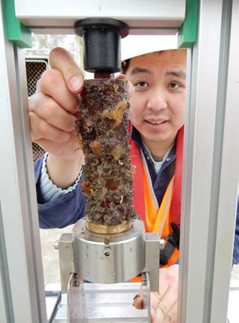
Together with his industry partners Andrew tackles practical issues of biofouling and corrosion.
ABOVE: Fellow CMatP Dr Anna Paradowska and Dr Wyman Zhuang with Andrew. BELOW: Andrew with metallurgy expert George Vander Voort.
MATERIALS AUSTRALIA
Our Certified Materials Professionals (CMatPs)
The following members of Materials Australia have been certified by the Certification Panel of Materials Australia as Certified Materials Professionals.
They can now use the post nominal ‘CMatP‘ after their name. These individuals have demonstrated the required level of qualification and experience to obtain this status. They are also required to regularly maintain their professional standing through ongoing education and commitment to the materials community.
We now have over one hundred Certified Materials Professionals who are being called upon to lead activities within Materials Australia. These activities include heading special interest group networks, representation on Standards Australia Committees, and representing Materials Australia at international conferences and society meetings.
To become a CMatP visit our website: www.materialsaustralia.com.au
Prof Yun Liu ACT
Dr Takuya Tsuzuki ACT
Prof Klaus-Dieter Liss
Mr Debdutta Mallik MALAYSIA Mr Dashty Akrawi
Maree Anast
Megan Blamires
Elena Pereloma
Sophie Primig
Simon Ringer
Richard Roest
Dr Peter Ford
Mrs Liz Goodall
Mr Bruce Ham
Ms Edith Hamilton
Mr Hugo Howse
Mr Long Huynh VIC
Dr Amita Iyer VIC
Dr John Kariuki VIC
Mr Robert Le Hunt VIC
Dr Thomas Ludwig VIC
Carl Strautins
Dr Roger Lumley VIC
Mr Michael Mansfield VIC
Dr Gary Martin VIC
Dr Siao Ming (Andrew) Ang VIC
Dr Eustathios Petinakis VIC
Mr Paul Plater VIC
Dr Dong Qiu VIC
Mr John Rea VIC
Dr M Akbar Rhamdhani VIC
Michael Chan
Andrew Dark
Ian Dover
Oscar Duyvestyn
John Edgley
Dr Jayantha Epaarachchi
Jeff Gates
Miss Mozhgan Kermajani
Dr Andrii Kostryzhev
Mr Jeezreel Malacad
Dr Alan McLeod
Mr Aaron Middleton
Dr Jason Nairn
Mr Bhavin Panchal
Mr Bob Samuels
Mr David Schonfeld
Ms Ingrid Brundin
Mr Neville Cornish
A/Prof Colin Hall
Mr Mikael Johansson
Dr Peter Kentish
Mr Rahim Kurji
Mr Greg Moore
Mr Andrew Sales
Thomas Schläfer
Dr Christiane Schulz
Ms Deborah Ward
Mr Ashley Bell
Mr Kok Toong Leong
Dr Ivan Cole
Dr John Cookson
Dr Evan Copland
Dr Malcolm Couper
Miss Ana Celine Del Rosario
Dr Yvonne Durandet
Dr Mark Easton
Dr Rajiv Edavan
Dr Christine Scala VIC
Dr Vadim Shterner VIC
Mr Mark Stephens VIC
Dr Graham Sussex VIC
Mr Pranay Wadyalkar VIC
Mr John Watson VIC
Dr Wei Xu VIC
Dr Sam Yang VIC
Mr Ashley Blackburn WA
Mr Graeme Brown WA
Mr Graham Carlisle WA
Mr John Carroll WA
Mr Sridharan Chandran WA
Mr Conrad Classen WA
Mr Chris Cobain WA
Ms Jessica Down WA
Mr Jeff Dunning WA
Mr Stuart Folkard WA
Prof Vladimir Golovanevskiy WA
Mr Chris Grant WA
Dr Cathy Hewett WA
Mr Paul Howard WA
Dr Paul Huggett WA
Mr Biju Kurian Pottayil WA
Mr Mathieu Lancien WA
Dr Yanan Li WA
Mr Michael Lison-Pick WA
Mr Ben Miller WA
Dr Brian Mubaraki WA
Mr Sadiq Nawaz WA
Dr Evelyn Ng WA
Mr Deny Nugraha WA
Mr Stephen Oswald WA
Mrs Mary Louise Petrick WA
Mr Johann Petrick WA
Mr Stephen Rennie WA
Mr James Travers WA
CHINA
NSW
NSW
NSW
NSW Dr
Carter NSW
Ceguerra NSW
Chau NSW
Cheng NSW
Crick NSW
Du Toit NSW Dr Azdiar MCGazder NSW Mr Buluc Guner NSW Dr
Hellier NSW Prof
Hoffman NSW Mr
Hussain NSW Mr
Krismer NSW Prof Jamie Kruzic NSW Prof Huijun Li NSW Prof
Linton NSW
Mackay-Sim NSW Dr
NSW Dr Warren McKenzie NSW Dr
NSW Dr
NSW
NSW A/Prof
NSW Dr
NSW Prof
NSW Dr
NSW Mr
NSW Dr
NSW
NSW Mr
NSW Mr
NSW Ms
NSW Mr
NSW Dr
NSW Dr
NSW Dr
NSW Dr
NSW Mr
NT Mr
QLD
QLD Mr
QLD Dr
QLD
QLD
QLD
QLD Dr
QLD
QLD
QLD
QLD
QLD
QLD
QLD
Ms
Ms
Dr Todd Byrnes
Phillip
Dr Anna
Mr Ken
Dr Zhenxiang
Mr Peter
Prof Madeleine
Alan
Mark
Muhammad
Simon
Valerie
Mr Rodney
Matthew Mansell
David Mitchell
Anna Paradowska
Prof
Gwenaelle Proust
Sameer Sameen
Luming Shen
Mr Sasanka Sinha
Alan Todhunter
Judy Turnbull
Jeremy Unsworth
Philip Walls
Rachel White
Alan Whittle
Richard Wuhrer
Payam Ghafoori
Prof Richard Clegg
Mr
Mr
QLD
QLD
QLD
SA
SA
SA
SA
SA
SA
SA
SA
SA
SA
SA
SCOTLAND
SINGAPORE
VIC
VIC
VIC
VIC
VIC
VIC
VIC
VIC
VIC
VIC
VIC
VIC
VIC
20 | JUNE 2020 BACK TO CONTENTS WW W.M ATERIALSAUSTRALI A COM AU
Why You Should Become a Certified Materials Professional
Source: Materials Australia
Accreditation as a Certified Materials Professional (CMatP) gives you recognition, not only amongst your peers, but within the materials engineering industry at large. You will be recognised as a materials scientist who maintains professional integrity, keeps up to date with developments in technology, and strives for continued personal development.
The CMatP, like a Certified Practicing Accountant or CPA, is promoted globally as the recognised standard for professionals working in the field of materials science. There are now well over one hundred CMatPs who lead activities within Materials Australia. These activities include heading special interest group networks, representation on Standards Australia Committees, and representing Materials Australia at international conferences and society meetings.

Benefits of Becoming a CMatP
• A Certificate of Membership, often presented by the State Chapter, together with a unique Materials Australia badge.
• Access to exclusive CMatP resources and website content.
• The opportunity to attend CMatP only networking meetings.
• Promotion through Materials Australia magazine, website, social media and other public channels.
• A Certified Materials Professional can use the post nominal CMatP.
• Materials Australia will actively promote the CMatP status to the community and employers and internationally through our partner organisations.
• A CMatP may be requested to represent Materials Australia throughout Australia and overseas with Government, media and other important activities.
• A CMatP may be offered an opportunity as a mentor for student members.
• Networking directly with other CMatPs who have recognised levels of qualifications and experience.
• The opportunity to assume leadership roles in Special Interest Networks to assist in the facilitation of new knowledge amongst peers and members.
What is a Certified Materials Professional?
A Certified Materials Professional is a person to whom Materials Australia has issued a certificate declaring they have attained all required professional standards. They are
recognised as demonstrating excellence and possessing special knowledge in the practice of materials science and engineering through their profession or workplace. A CMatP is prepared to share their knowledge and skills in the interest of others, and promotes excellence and innovation in all their professional endeavours.
The Criteria
The criteria for recognition as a CMatP are structured around the applicant demonstrating substantial and sustained practice in a field of materials science and engineering. The criteria are measured by qualifications, years of employment and relevant experience as evidenced by the applicant’s CV or submitted documentation.
Certification will be retained as long as there is evidence of continuing professional development and adherence to the Code of Ethics and Professional behaviour.
Further Information
For further information on becoming a CMatP, contact Materials Australia today: on +61 3 9326 7266 or imea@ materialsaustralia.com.au, or visit our website: www. materialsaustralia.com.au.
• Induction hardening to 400 Dia x 4000 Long (External), 200 Dia x 200 Long (Internal).
• High & low frequency induction generators to suit required hardening depth.
• Flame hardening to 650 Dia.
• Tooth by tooth flame or induction hardening of gears & sprockets to 3500 OD using standard or specially designed inductors or burners.
WW W.M ATERIALSAUSTRALI A COM AU BACK TO CONTENTS 21 | JUNE 2020 MATERIALS AUSTRALIA
GLOBAL STEEL HEAT TREATMENT FLAME & INDUCTION HARDENING 3 Stanton Road, Seven Hills NSW 2147 T: (02) 9624 6270 F: (02) 9674 6215 E: globalheattreatment@bigpond.com CMatP
Professor Nikki Stanford
Source: Sally Wood
phenomena in titanium, and magnesium texture development.
Professor Stanford is particularly well known for her light metals research portfolio, and in 2015 was awarded the Helmholtz-Zentrum Geesthacht’s Magnesium Award for international magnesium researcher of the year.
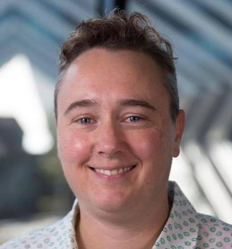
Q&A with Professor Stanford
Professor Stanfordtook time out of her busy schedule to answer a few questions for Materials Australia magazine.
Professor Nikki Stanford is a Research Leader in University of South Australia’s Future Industries Institute (FII). The FII was established with a new research culture in mind - one deeply engaged with industry, with the end goal of building economic growth through relevant innovation and industry partnership.
The Institute reflects the University’s strategic ambition to be Australia’s University of Enterprise which engages fully with the professions and industry globally, whose research is informed, leading edge and relevant. FII continues to forge national and international research partnerships, in new industries and technologies, that address real world issues. Their goal is to support a creative and engaged culture, and to help develop a sustainable ecosystem in which innovative, complex, growth-focused industries thrive.
Professor Stanford’s niche in the materials research field has been focused on bridging the gap between engineering and science, by applying a broad range of advanced characterisation techniques to ‘real world’ problems, such as fatigue, light-weighting and casting.
Before joining FII, Professor Stanford held research positions with Imperial College London, the University of Manchester, Deakin University and Monash University. She has studied a broad range of materials research topics, including casting defects in nickel single crystal turbine blades, shape memory steels, phase transformation
Why (and how) did you decide to embark on a career in Materials Science?
Materials science is the perfect mix of science and engineering. I get to use expensive microscopes and do some really exciting science, and it all ends up being useful to someone. Although I started out doing mostly hard materials such as steels, I’m increasingly getting involved in collaborative research looking into polymers, surface science, energy storage, medical devices and computational science.
Can you describe the projects you’re currently working on?
Outside of my research, I also teach in the undergraduate course on materials science, which is a compulsory for all engineers. I’m pretty passionate about it. We get one opportunity to instil the most
important principles of materials into our future engineers. This is to ensure that they understand the true nature of the materials that they are using. I’m also the chair of the Microscopy Australia Education Committee.
Our main focus at the moment is the expansion of our online training tool called MyScope https://myscope.training. It’s the largest online microscopy training tool, and we get about 100,000 unique visitors every year, from all over the world. It’s a great project to be part of—I really enjoy it.
What
do you enjoy most about your research?
I enjoy the small amount of lab time I get. I’ve enjoyed doing 3D printing and working with my digital technologies colleagues on Industry 4.0 projects, but ultimately, what I enjoy most is being on an expensive instrument taking beautiful micrographs. I wish I could be in the lab all the time.
Coating and Repair of Additive Manufactured Components
Professor Stanford is part of a research project that is investigating the development of laser clad and 3D printed structures, as well as other potential application technologies, for use in the mining and oil and gas industries.
The structures will be designed to resist abrasion, erosion, impact and corrosion (both chemical and microbially induced). The projects will include design, investigation of process parameters,

WOMEN IN THE INDUSTRY
22 | JUNE 2020 BACK TO CONTENTS WW W.M ATERIALSAUSTRALI A COM AU
The University of South Australia’s Industry 4.0 Testlab. Image courtesy of the University of South Australia.
advanced feedback mechanisms and control, measurement of properties, as well as the study of interface behaviour by advanced electron microscopy. Along with the University of South Australia’s industry partners, LaserBond and Santos, the project also includes hands-on training experience for several PhD students.
Surface Engineering for Advanced Materials
Professor Stanford is one of the chief investigators for the Surface Engineering for Advanced Materials (SEAM) ARC Training Centre. SEAM targets the training of early career researchers in an industrial context. The proposed area of surface engineering for advanced materials is a core need in all manufacturing sectors that control the efficiency, productivity and sustainability of Australian industry.
This project aspires to be the model centre that integrates industry-university cooperation for applied training within an industrial setting. This Centre desires to be the nexus for an international collaborative network. The Centre pursues ambitious outcomes that are reflected in terms of industry-fit researchers and commercial benefits for industry. The spectrum of applications being addressed ranges from thin films to thick coatings and additive layered materials.
This is the first Training Centre of its kind, with a specific focus on surface engineering across (i) very thin films less than 10 μm, (ii) coatings less than 250
μm, and (iii) thick overlays up to tens of millimetres thick. The third category encompasses additive manufacturing (AM) since this is, fundamentally, a layerby-layer material deposition process. Application fields include: biomaterials, corrosion, graphene layering, machining, cutting, grinding, thick coatings for heavy industries such as mining, high temperature coatings, laser metal deposition for materials repair, additive manufacturing for aerospace, and Industry 4.0 manufacturing processes.
For further information, visit: https://arcseam.com.au
Industry 4.0 Testlab
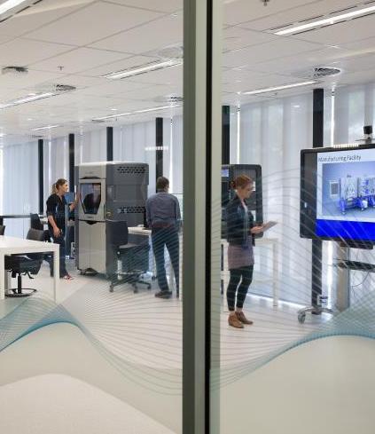
Professor Stanford is the Director of the University of South Australia’s Industry 4.0 Testlab. The Testlab has established to demonstrate Industry 4.0 methodologies and practices, and includes practical laboratory-based capabilities and a pilot scale manufacturing demonstration. The Testlab has a particular focus on the defence sector, and is also highly relevant to the space, mining, electronics, food and agriculture, and automotive industries.
A key objective of the Testlab is engagement with small and medium enterprises (SMEs), introducing them to a broad range of Industry 4.0 strategies, methodologies and approaches. This includes demonstrating how these methods can be adopted by industry to enhance productivity, competitiveness and profitability. The Testlab provides local SMEs, and high-tech start-ups, with
otherwise unattainable access to these smart factory technologies.
For further information, visit: https:// www.unisa.edu.au/research/testlab/
Other Projects
Cluster Hardening of Metastable Steel Alloys Produced by Thin Strip Casting
The goal of this project is to generate sufficient knowledge to apply strip casting to a wider range of steel grades. Direct strip casting is an emerging green technology that reduces the energy required to process liquid steel into thin sheet product by up to 90%.
Development of Novel High Performance Aluminium Alloys Containing Scandium
Over 30 million tonnes of high performance aluminium alloys are produced per annum. This project aims to develop a new generation of alloys that contain scandium. SScandium is beneficial in the improvement of the bulk properties of aluminium, but its high cost has restricted research. Australia has the largest deposit of scandium in the world, and the Australian mining company, Clean TeQ, has developed a sustainable extraction technology to capitalise on this resource. A fundamental understanding of the beneficial effects of scandium will expedite rapid developments in these new alloys.
WOMEN IN THE INDUSTRY
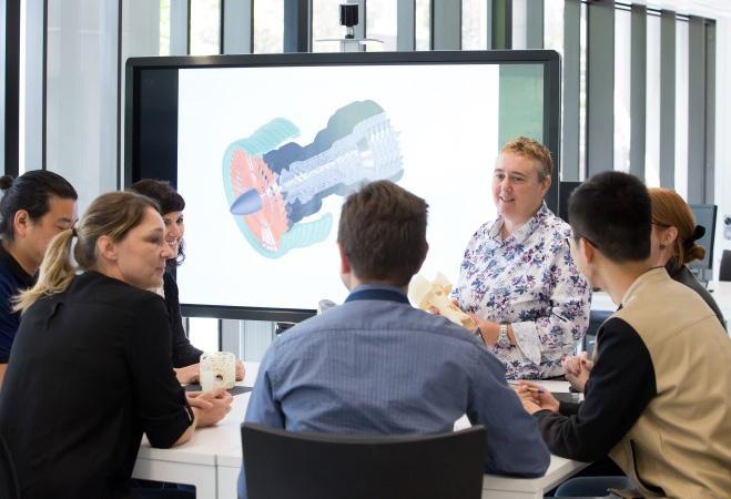
Professor Nikki Stanford addresses a group of researchers at Industry 4.0 Testlab. Image courtesy of the University of South Australia.
WWW.MATERIALSAUSTRALIA COM AU BACK TO CONTENTS JUNE 2020 | 23
Inside the University of South Australia’s Industry 4.0 Testlab. Image courtesy of the University of South Australia.
When One Door Opens: Monash Student Develops 3D Printed Key to Prevent COVID-19 Spread
Source: Sally Wood
A Monash University engineering student has used 3D printing to develop a cheap and safe plastic tool that can open doors and push buttons, eliminating the need for hand contact on potentially contaminated surfaces in the era of COVID-19.
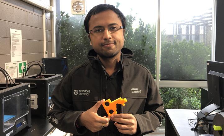
PhD student, Muthu Vellayappan from Monash University’s Department of Materials Science and Engineering, is the person responsible for inventing the simple tool that can help people eliminate their direct contact with door handles, lift buttons, ATM digits, toilet flushers and hand dryers, and other areas where contamination might be present. These kinds of tools are essential when it comes to limiting the spread of COVID-19.
After watching videos online of people sneezing and spitting into their hands, and deliberately touching door handles and .lift buttons, Vellayappan jumped into the lab, in early March 2020, to design and test the tool he calls a ‘Safety Key’. The ‘Safety Key’ helps to slow the transmission of viruses in the community.
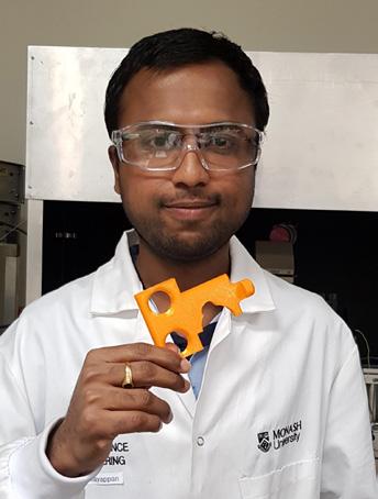
Under the guidance of Professor Neil Cameron, Head of the Department of Materials Science and Engineering at Monash University, Vellayappan made 30 prototypes of the key, which he circulated to Monash staff, and a further 10 copies to a neighbouring hospital.
Vellayappan said the key is multifunctional and can work on L-shaped and U-shaped door handles which are commonly found at shopping centres, hospitals and universities, and in places of high pedestrian traffic, such as traffic stops, tram and bus buttons, ATMs, and lifts.
He is also looking at further modifications to the key so that it can be used on the handles of supermarket trolleys.
Above all, the cost to produce one of the keys, using 3D printing, is less than $1, including materials and manufacturing. With industry support or additional funding, this cost could be reduced if the design is injection moulded for mass production. Additionally, while it currently takes between 60 and 90 minutes to create
a single key, this timeframe could be significantly reduced if the key is produced en-masse.
While the main motivation to create the key was to stop the community transmission of COVID-19, Vellayappan says the key can also prevent other viruses and bacteria spreading from surface-to-person in areas of high public frequency.
“The first design was extremely bulky and had only one groove, which wasn’t sufficient for the different sizes of L-shaped door handles we have in our community,” Vellayappan said.
“With a size less than that of a mobile phone, I was able to adjust the key to fit a number of door handles across the University, allowing me to open and close each door without making contact with the handle,” Vellayappan continued.
“Usually, we are prone to infection in a common area, like shopping centres and public bathrooms, where L-shaped door handles are common. Cleaning the keys is also very simple – because they’re made from plastic, a gentle wash in warm water with soap will do the job,” Vellayappan explained.
Vellayappan isn’t seeking a patent for his product, and has willingly shared his design with people across the world who have access to 3D printers.
“It’s important now for people across the world to have immediate access to tools that can help slow the spread of this virus. People’s lives depend on any little innovation – especially one such as the ‘Safety Key’ which is cost-effective and easy to produce,” Muthu said.
Professor Cameron commended Muthu’s innovation: “This is a great example of how resourceful and creative our PhD students are. I hope that Muthu’s ‘Safety Key’ is adopted widely and helps reduce community spread of COVID-19.”
INDUSTRY NEWS
24 | JUNE 2020 BACK TO CONTENTS WW W.M ATERIALSAUSTRALI A COM AU
PhD student, Muthu Vellayappan, has invented a ‘Safety Key’ that can help people eliminate contact with potentially contaminated surfaces in the era of COVID-19.
Ultrafast Probing Reveals Intricate Dynamics of Quantum Coherence
Source: Sally Wood
Ultrafast, multidimensional spectroscopy unlocks macroscopic-scale effects of quantum electronic correlations.
Researchers have found that low-energy and high energy states are correlated in a layered, superconducting material LSCO (lanthanum, strontium, copper, oxygen).
Exciting the material, with an ultrafast (<100fs) beam of near-infrared light, produces coherent excitations lasting a surprisingly ‘long’ time of around 500 femtoseconds, originating from a quantum superposition of excited states within the crystal.
The strong correlation between the energy of this coherence, and the optical energy of the emitted signal, indicates a coherent interaction between the states at low and high energy.
This kind of coherent interaction is the root of many intriguing and poorly-understood phenomena displayed by quantum materials.
It is one of the first applications of multidimensional spectroscopy to study correlated electron systems, such as hightemperature superconductors.
The intriguing magnetic and electronic properties of quantum materials hold significant promise for future technologies. However, controlling these properties requires an improved understanding of the ways in which macroscopic behaviour emerges in complex materials with strong electronic correlations.
Potentially useful electric and magnetic properties of quantum materials with strong electronic correlations include: Mott transition, colossal magnetoresistance, topological insulators, and hightemperature superconductivity.
Such macroscopic properties emerge out of microscopic complexity, rooted in the competing interactions between the degrees of freedom (charge, lattice, spin, orbital, and topology) of electronic states.
While measurements of the dynamics of excited electronic populations have been able to give some insight, they have largely neglected the intricate dynamics
of quantum coherence.
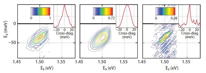
In a new study, researchers applied multidimensional coherent spectroscopy to the challenge for the first time, utilising the technique’s unique capability to differentiate between competing signal pathways, selectively exciting and probing low-energy excitations.
Researchers analysed the quantum coherence of excitations produced by hitting LSCO (lanthanum, strontium, copper and oxygen) crystals with a sequence of tailored, ultrafast beams of near-infrared light lasting less than 100 femtoseconds
This coherence has unusual properties, lasts a surprisingly ‘long’ time of around 500 femtoseconds, and originates from a quantum superposition of excited states within the crystal.
“We found a strong correlation between the energy of this coherence and the optical energy of the emitted signal, which indicates a special coherent interaction between the states, at low and high energy, in these complex systems,” said study author Jeff Davis from Swinburne University of Technology.
Because the number of available excitations affects the band structure of a crystal, the effective energy structure changes transiently during measurement, which links low-energy excitations and optically excited electronic states.
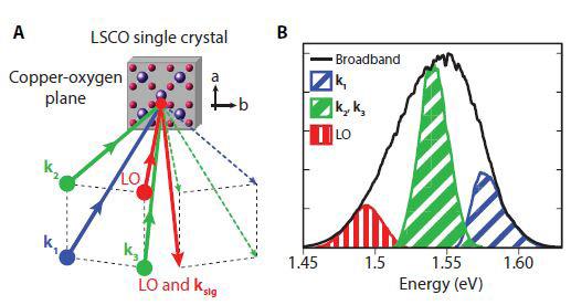
The study demonstrated that multidimensional coherent spectroscopy can interrogate complex quantum materials in unprecedented ways. Furthermore, the results demonstrate that multidimensional coherent spectroscopy is a powerful tool in the study of electronic correlations, and
opens the door to addressing, directly, the quantum-coherent states of many-body matter.
As well as representing a major advancement in ultrafast spectroscopy of correlated materials, the work has wider significance in optics and photonics, chemistry, nanoscience, and condensedmatter science.
The research paper, ‘Persistent coherence of quantum superpositions in an optimally doped cuprate revealed by 2D spectroscopy’, was published in Science Advances.
Within FLEET, Jeff Davis uses ultrafast spectroscopy to study and control the microscopic interactions in 2D materials and how they lead to macroscopic behaviour.
In FLEET’s third research theme, lighttransformed materials, systems are temporarily driven out of thermal equilibrium in order to investigate the qualitatively different physics displayed, and new capabilities for dynamically controlling their behaviour.
FLEET is an Australian Research Councilfunded research centre bringing together over a hundred Australian and international experts to develop a new generation of ultra-low energy electronics.
INDUSTRY NEWS
2D spectrum showing energy difference between the states in the quantum superposition, shown before, during and after pulse overlap.
WW W.M ATERIALSAUSTRALI A COM AU BACK TO CONTENTS 25 | JUNE 2020
Three excitation pulses with wave vectors k1, k2, and k3 form three corners of a box with 4th pulse (local oscillation; LO) on the fourth corner.
The Power of Sound Waves Making Noise with New Research
Source: Sally Wood
The possibilities for sound wave technology are constantly being realised, with major advances being made through RMIT research.
High-frequency sound waves, inaudible to the human ear, are being used in myriad applications, from building advanced materials to nanoscopic drug delivery. After 10 years of research, Distinguished Professor Leslie Yeo, and his team at the Micro and Nanophysics Research Laboratory, say they are only scratching the surface of understanding this technology’s full potential.
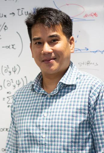
“We keep discovering new phenomena – mostly by accident,” Yeo said. “This is because no one has been crazy enough to couple high-frequency sound waves into fluids and materials – we’re one of the very few groups in the world doing this work.”
“In addition to building practical technology, we want to advance fundamental scientific knowledge as a foundation upon which we can better design devices,” Yeo continued.
Yeo and his team explore sound waves at high frequencies, above 10 MHz. With low frequency sound waves, sonochemical reactions are driven by the violent implosion of air bubbles – a process known as cavitation. But at higher frequencies, cavitation is largely absent, indicating there is a completely new and unknown mechanism behind the reactions.
The sound waves are generated on a microchip, to precisely manipulate fluids or materials at nano scale – down to atoms and molecules.
Since beginning the research, Yeo said his team has had to challenge a number of classical physics theories, at least when it comes to explaining what they see.
“We have developed theories that have been controversial, such as how fluids behave when vibrated from beneath by the sound waves,” Yeo said. “There are long-held classical theories, from the mid-1800s, on how these waves should behave, but these theories just don’t explain what we see.”
The team’s recent foray into vibrating nanomaterials and crystals, with these sound waves, is equally intriguing. It is especially puzzling that the sound energy, with wavelengths of hundreds of micrometres, can manipulate entities such as atoms or molecules, which are almost a million times smaller.
Beyond fundamental discoveries, Yeo’s team is also translating the technology for practical benefit.
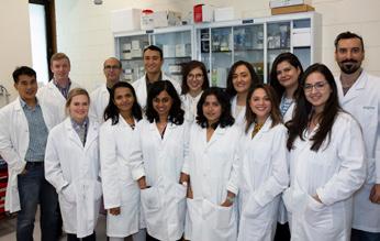
Using their sound wave technology, they have designed a revolutionary nebuliser, called ‘Respite’, that can administer precise doses of the next generation of drugs, such as immunotherapies, to patients with debilitating lung conditions.
‘Respite’ is cheaper, faster, more portable, and has greater delivery rates than standard nebulisers.
But more importantly, it can deliver large molecules – something current nebulisers cannot do. This opens the potential to painlessly administer vaccines.
Not only is Respite painless, it is also more effective than standard nebulisers. Respite is able to deliver more drugs into the lungs by using sound waves to generate a fine aerosol mist containing the drug molecules.
“The problem with conventional inhalers is that most of the drug is deposited in the mouth and doesn’t actually get to the lungs, which isn’t a problem if the drugs are cheap, but it is when they are very expensive, such as the new immunotherapy drugs,” Yeo said.
“Unlike one-size-fits-all inhalers, Respite allows the dose to be adjusted based on
a patient’s size, age, gender, physiological profile and disease severity, thereby allowing a greater percentage of the drug to get into the lungs.”
“Also, Respite doesn’t require inhalation to generate the mist, like traditional inhalers, which can be a problem for people already suffering compromised lung function,” Yeo explained.
The nebuliser has been successfully tested in clinical trials, and showed it is capable of delivering more medicine, more quickly to the lungs.
Discussions are well advanced with an industry partner for the commercialisation of the Respite nebuliser, with hopes it could be on the market within two years.
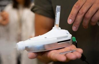
INDUSTRY NEWS
Yeo and his team at the Micro and Nanophysics Research Laboratory.
‘Respite’ generating a fine mist containing larger molecules.
26 | JUNE 2020 BACK TO CONTENTS WW W.M ATERIALSAUSTRALI A COM AU
Distinguished Professor Leslie Yeo.
Synthetic Material Could Help Heal Injured Tendons and Ligaments
Source: Sally Wood
Researchers from the University of Sydney have collaborated with Columbia University and the University of Erlangen-Nuremberg to develop a synthetic material to assist in the regeneration of injured tendons and ligaments. Australia’s love of sport means it has one of the highest rates of knee anterior cruciate ligament (ACL) injury and reconstruction in the world.

Worldwide, the costs of tendon and ligament rupture repair and surgery revision represent tens of billions of dollars of the clinical orthopaedic market. A team of biomedical engineering researchers from the University of Sydney, working with the Regenerative Engineering Laboratory at Columbia University and the FAU ErlangenNuremberg Institute of Medical Biotechnology (Germany), is hoping to improve the outcomes of tendon and ligament repair, by developing a new synthetic scaffold for their regeneration. Led by the Head of the Biomaterials and Tissue Engineering Research Unit at the University of Sydney and Director of the Australian Research Centre for Innovative BioEngineering, Professor Hala Zreiqat, and working with postdoctoral researcher Dr Young No, the researchers are the first to develop and patent novel fibre-reinforced hydrogel scaffolds, a synthetic substance that has the ability to mimic and replace human tendon, and ligament tissue. Previous synthetic tendon grafts have demonstrated suboptimal tissue ingrowth and synovitis, due to wear particles from fiber-to-fiber abrasion. In this research, a novel fiber-reinforced hydrogel (FRH) is presented, that mimics the hierarchical structure of the native human tendon for synthetic tendon graft material.
“Ruptures to tendons and ligaments mostly occur in accidents and when playing sport. Worldwide, and particularly in Australia, there is an immense clinical need for the development of readily available, off-the-shelf, mechanically strong, synthetic tendon scaffolds,” said Professor Zreiqat, from the ARC Centre for Innovative BioEngineering, School of
Biomedical Engineering and the Sydney Nano Institute.
“Conservative methods using immobilisation casts and movement restricting splints and braces often require several weeks of rehabilitation to achieve minimal functional recovery, while current implants carry a higher risk of rejection and infection,” Professor Zreiqat continued.
“Our technology hopes to fast-track the restoration of tendons’ and ligaments’ mechanical function, and support the growth of collagen tissue, without compromising the body’s biological response.”
Tested on patellar tendon models in rats, the synthetic scaffold has been developed with a stress resistance and water volume similar to real tendons and ligaments, allowing for the improved in-growth of collagen tissue.
“Until now, synthetic scaffolds have come with a significant risk of implant failure, as well as poor biological tissue integration and abrasion,” she said.
“Human tendons and ligaments are 70% water – they are complicated structures that include blood vessels, nerves and lymphatic vessels, and perform the task of linking bone to muscle and moving the body,” Professor Zreiqat continued.
“For synthetic scaffolds to be accepted by the body, their physical and chemical architecture must align with human tendons and ligaments.”
The researchers now hope to investigate the long-term behaviour of these scaffolds in both internal and external bodily conditions, as well as to observe tissue integration and biomechanics in larger animal models.
This research received financial support from the Australian Research Council, the Australian National Health and Medical Research Council, the Rebecca L. Cooper Medical Research Foundation, and the Australian Centre for Microscopy and Microanalysis at University of Sydney with technical support for Scanning Electron Microscopy analysis.
WW W.M ATERIALSAUSTRALI A COM AU BACK TO CONTENTS 27 | JUNE 2020
INDUSTRY NEWS
The research hopes to improve the outcomes of sport injury surgeries.
Australian Innovation Leads to Sustainable Alternative for Architectural Hardwoods
Source: By Dr. Cameron Chai
Researchers have long sought to recreate natural materials like spider’s silk and human bone with varying degrees of success. Australian company 3RT has gone one better, successfully manufacturing appearance-grade hardwoods using a process that takes just 1 day, where mother nature would take 100’s of years. What’s even more significant is that the products are sustainable and ecologically friendly.
While there are other products on the market such as plywood and MDF (medium density fibreboard), 3RT have commercialised a product that addresses the other end of the market, i.e. high-end architectural and designer timber products. What really makes their product stand apart are its environmentally friendly credentials. 3RT’s Designer Hardwood
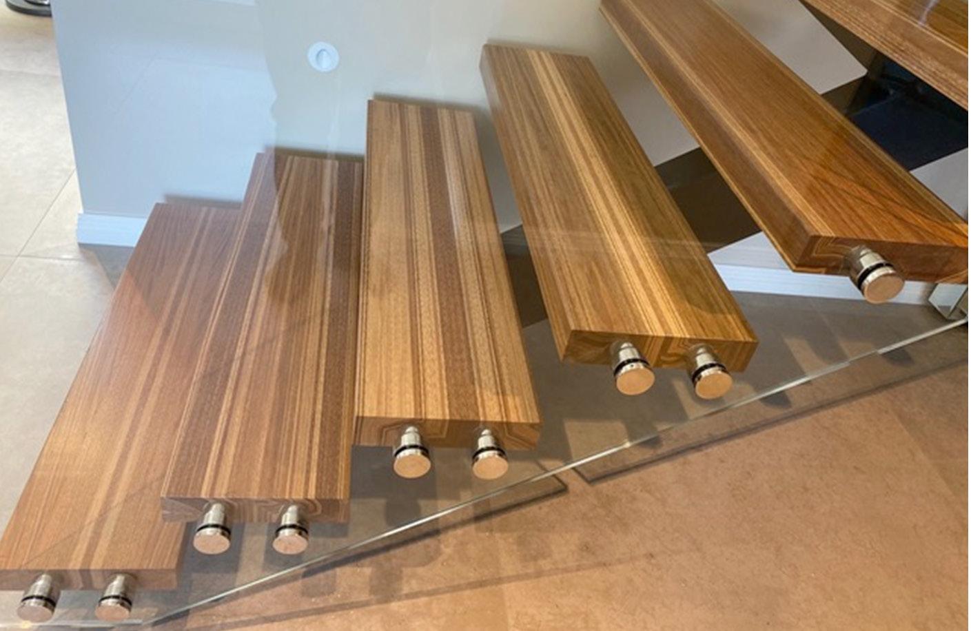
is based on wood waste materials. Furthermore, Designer Hardwood uses water-based adhesives unlike the phenolics and other resins used in other reconstituted wood products. In doing so, it also satisfies the company’s core values, reduce, reuse and recycle.
Designer Hardwood, is the product of several years of development work by 3RT. It looks, feels and behaves just like naturally sourced tropical hardwood, retaining the texture and warmth of the natural material. In fact, it has growth rings to give it grain, but owing to the fact it is man-made, it doesn’t have cracks or splits that may render certain sections unusable. It can be cut, machined and coated just like any other hardwood and is probably easier to work with than the natural analogue as it doesn’t have any nots and is more consistent.
3RT formed in 2014 with the idea of creating a product from wood residues
from trees that are not suitable for producing sawn quality timber. These trees may be sourced from councils who need to remove trees, many of which may be sick or dangerous, or excess trees from timber plantations which effectively makes them waste products.
However, this is not a typical story of how an industry insider identifies a problem, finds a solution and commercialises it. Rather, 3RT had an idea and almost no relevant industry expertise. As a result, they had to form strategic partnerships with outsiders to turn the concept into a reality.
Solving The Materials Problem
Peter Torreele, Managing Director of 3RT explained, “after initially contacting wood experts, 3RT looked outside the box and began working with materials experts at Flinders University to solve the physical problem of how to turn wood waste
INDUSTRY NEWS
28 | JUNE 2020 BACK TO CONTENTS WW W.M ATERIALSAUSTRALI A COM AU
materials into attractive timber.” With the specific requirement to develop an environmentally friendly product, 3RT and Flinders set about developing a process using a water-based, formaldehyde-free “Nano-glue” that biomimics the structure of a natural tree in hours.
They then tackled the next issue of designing an industrial process to create the final product. They achieved this by combining pressure and temperature to densify and the materials and cure the resin, in a process that takes merely minutes.
3RT also worked with TAFE SA, whom they supplied with materials to work with so they could see how the material behaved and performed. They used this feedback to further refine the material to make it as close to the Mother Nature’s own product.
Solving The Production Problem
Based on the process developed by 3RT, they built a pilot unit that is now located at their Innovation Centre in Adelaide. They then partnered with Bosch Manufacturing Solutions to design and optimise the future manufacturing facility. The fact that this had never been done before was probably a blessing in disguise. It allowed people with expertise form other fields such as automotive to offer fresh ideas on how the production process could be designed.
Andrew Bartlett, Manager Strategic Projects at Bosch Manufacturing Solutions said, “we had never seen a project like this before as we normally operate in the advanced manufacturing and medtech space. The more we looked at it, the more we realised the project had merit and although the application was very different, the basic concepts were still the same and could benefit from our expertise in sensors, robotics, automation, materials handling and data processing.”
The team from Bosch designed a highly sophisticated, automated production workflow that relies heavily on constantly processing data acquired from throughout the process dealing with over 100 process parameters. The process is so tightly monitored that it can take into account the variances in natural trees that act as the raw material and adjust the process accordingly to achieve greater than 99% product conformity in the finished product. It even has the intelligence to learn and take into account the changes that take place for future occurrences. Furthermore, the high levels of automation effectively
eliminate operator error from the 2 people required to run a shift, contributing to product consistency.
The process is able to produce hardwood slabs 500x270x2600mm. Hardwood slabs this size have not been available for a very long time. The plant itself is scalable with a production capacity of 6-10,000m3/year.

“One of the beauties of our system is that the output is independent of the input material. The system is robust enough and smart enough to make adjustments to the process such that it can even convert softwoods into hardwoods”, said Peter Torreele.
Sustainability
As mentioned, the raw materials are primarily waste products and the other materials are non-toxic and recyclable. The development of Designer Hardwood is also somewhat timely with hardwoods getting scarcer due to protection of native forests . This will no doubt continue to drive prices up, while at the same time governments look to implement legislation to outlaw illegal logging.

Sawmills that process naturally occurring hardwoods are like CNC machining stations which take large billets and machine them down to smaller, tailored size slabs. This results in a lot of waste. In the case of a hardwood sawmill, they typically run at 30-32% efficiency. 3RT’s process is the opposite. By using a bottom up manufacturing approach there is essentially no waste from the production process, while the tropical hardwood trees are allowed to flourish and the associated wildlife habitats can remain intact.
Commercialising the Technology
We all accept that buying sustainable alternatives is better for the environment, however, we also know that doing the right things for the environment often comes with a premium price. This is not the case for Designer Hardwood because 3RT does not want to charge an “ecopremium”.
While Designer Hardwood is commercially available in limited quantities through a handful of select lighthouse customers, Peter explains this is more to see how to determine the optimum routes to market. Their aim is to work with international partners to set up production facilities around the world and to licence the technology.
3RT finished the demonstration plant in Adelaide in 2019. There are plans to build a larger commercial plant in the near future. The existing plant was built so that 3RT can work with customers to refine the manufacturing process, tailoring it to their own, locally sourced wood fibres. Once the proof of concept has been completed, the client can be provided with a fully functional production plant delivered to their site and pre-optimised with their own specific set of production parameters streamlining the path to commercial viability.
There are a number of companies that have already expressed interest in Designer Hardwood and 3RT’s innovative process of turning a waste product into a sustainable, high-value product. Hopefully this will be the next chapter in another Australian success story with production plants and an excellent case study strategic partnerships can be used to marry different skillsets across industries and scientific fields for a common outcome.
WW W.M ATERIALSAUSTRALI A COM AU BACK TO CONTENTS 29 | JUNE 2020 INDUSTRY NEWS
Bridging the Gap to the Synchrotron
The Australian Synchrotron (AS) is a critical piece of research infrastructure. The synchrotron beamlines house high-end research facilities which simply cannot be replicated in a normal laboratory. In recent years several technologies have enabled instruments that close the gap to the synchrotron. Instruments that can easily be incorporated into onsite laboratories open up new research opportunities. In this article we take a look at some of these systems.
While the benefits to research of these facilities are undeniable, sometimes access can be an issue. Their sheer size and expense means we only have one in Australia. Unfortunately, running experiments can be cost prohibitive, while availability and logistics can also provide barriers.
Synchrotron Alternatives
While the power of a synchrotron may not be able to be replicated there are lab-based systems available that produce and utilise high intensity X-rays. These systems can provide data that results in similar analyses or can be a highly capable way of screening samples, helping you to decide which are the most important ones to measure at the synchrotron.
X-Ray Diffraction
XRD has been a staple technique for materials identification and analysis. Most commercially available systems use sealed X-ray tubes and are rated at 3kW, but don’t normally operate above 1.6kW (i.e. 40kV and 40mA). The Rigaku SmartLab using uses a Rotating Anode X-ray generator and can operate continuously at 9kW, producing almost 6 times more usable flux with the addition of purposedesign optics. Despite its higher power output it is no bigger than 3kW systems.
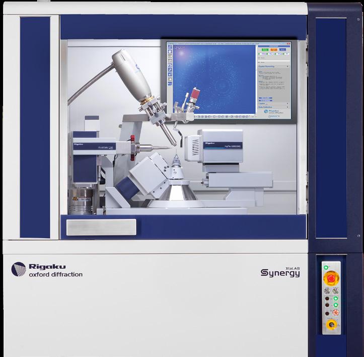
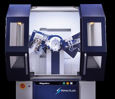
This system retains the same architecture as lower powered system, enabling it to run all the same experiments. The higher X-ray flux available with the SmartLab 9kW just means it can do it faster, resulting in higher throughputs, with a better chance of identifying trace components, especially when coupled with high-speed detectors like the HyPix range that use Hybrid pixel area detector (HPAD) technology. Given the life expectancy of a diffractometer, installing a system like this also better prepares your lab for future experiments on materials that you may have never thought of.
Similarly for crystallography researchers, in particular those working on single crystals, the Synergy-R from Rigaku Oxford Diffraction uses the same Rotating Anode technology and can also be married to high speed HPAD detectors for maximum sensitivity and throughput.
Micro X-Ray Fluorescence
XRF spectrometers typically use similar sealed X-ray tubes with a limited power output of 3-4kW. Sigray, pioneers in the X-ray imaging and analysis field have developed a revolutionary new X-ray source called Fine Anode Array Source Technology or FAAST. It incorporates micron-scale metal X-ray emitters that are embedded into a diamond substrate which provides optimal cooling and synchrotron-like performance.
FAAST is used in the AttoMap, X-ray fluorescence microscope. While a conventional XRF might produce an elemental map in tens of minutes, the AttoMap achieves this is just a
INDUSTRY NEWS
Source: By Dr. Cameron Chai, Dr. Nav Dhaliwal, Dr. Kamran Khajehpour, Peter Airey and Richard Trett, AXT Pty Ltd
9kW Rigaku SmartLab XRD.
30 | JUNE 2020 BACK TO CONTENTS WW W.M ATERIALSAUSTRALI A COM AU
XtaLAB Synergy-R single crystal diffractometer from Rigaku Oxford Diffraction, powered by a rotating anode X-ray source.
few seconds. Its sensitivity, down to the femtogram level is unrivalled by even techniques such as SEM with EDS. Furthermore, it also has the advantage over conventional XRFs in that it can also produce X-ray images.
The AttoMap is applicable to such things as coatings, thin films, metallomics, nanoparticles, contamination of advanced materials, semiconductors, forensics and geological materials.
X-Ray Absorption Spectroscopy
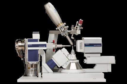
XAS, which encompasses XANES (X-ray absorption near edge structure) and EXAFS (Extended X-Ray Absorption Fine
Structure). This technique yields critical insights onto chemical states, such as oxidation states and electronic structure, such as bond lengths and electron geometry surrounding the atom. Utilising the same FAAST synchrotronlike X-ray source, this technique is now available in a lab-based system in the Sigray QuantumLeap. It is highly applicable to batteries, catalysts, fuel cells and solar cells.
Dynamic Micro Computed Tomography
While many lab-based micro-CT systems are able to carry out time lapse studies, continuous dynamic studies, also known as 4D CT are unique to the TESCAN DynaTOM. Previously restricted to the realms of synchrotrons, recent advances in X-ray source and detector technologies, combined with a unique gantry architecture and more intelligent software, the TESCAN DynaTOM is able to continuously scan samples under dynamic conditions, ensuring any specific event is not missed.
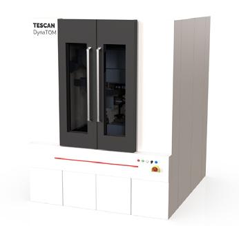
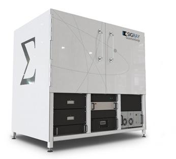
Ultraviolet (VUV) and EUV sources with ultrafast femtosecond pulses, tuneable wavelengths and photon energy only previously possible at synchrotrons can be used as the basis for a lab-based system. When paired with a suitable detector, ARPES (both spin and time resolved) is now a reality in a lab-sized system where it can aid in the development of solar cells, photocathodes and catalysis to spintronics, topological materials and quantum technologies.
Compact Light Source
The Lyncean CLS is a breakthrough technology that delivers synchrotron-like X-rays. Monochromatic, tuneable (8keV to 100keV) and high brightness it is similar in nature to a single beamline. It can be connected to end stations of your choice, thus providing a local synchrotron alternative.
At a fraction of the size and a fraction of the cost, it becomes feasible to have synchrotron-type capability in each major city. This could potentially overcome many of the issues with availability and logistics, in fact providing increased availability and access for researchers. It also opens up a lot of reasarch opportunities like studying fragile, short-lived materials or conducting ongoing long term experimentation.
Dynamic studies allow researchers and engineers to understand how materials behave under conditions that more closely resemble real life operating scenarios e.g. changing loads, flow or environments such as temperature. Such studies can rapidly accelerate the development pathway for a wide variety of engineering components.
Angle Resolved Photoemission Spectroscopy
ARPES is a surface sensitive analytical technique which, until recently, had also been only possible at the synchrotron. With advances in laser technology, the KM Labs Hyperion Vacuum
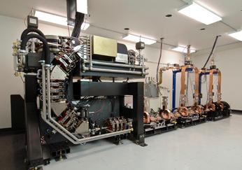
Summary
While The Australian Synchrotron has a defined place in Australian research, there are many systems that are currently available that bridge the gap between it and other common lab-based instruments. By incorporating more of these in research institutions, it is feasible that research outcomes could be accelerated. Whether these synchrotron alternatives produce high enough quality data, or simply act a screening tool for future synchrotron experiments they could potentially also reduce our reliance on the synchrotron.
INDUSTRY NEWS WW W.M ATERIALSAUSTRALI A COM AU BACK TO CONTENTS 31 | JUNE 2020
Lyncean Compact Light Source, a lab-sized system capable of producing synchrotron-like X-rays.
Sigray AttoMap X-ray fluorescence microscope.
Sigray QuantumLeap X-ray absorption spectrometer.
TESCAN DynaTOM dynamic microCT system.
XtaLAB Synergy-R optical configuration.
Time Resolved MicroCT in the Lab is Now a Reality
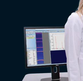 Source: By Dr. Cameron Chai, AXT Pty Ltd

MicroCT with its ability to nondestructively image materials in 3D is arguably the most exciting imaging modality in materials science. While some systems are able to carry out time lapse studies, TESCAN have upped the ante with the ability to perform dynamic CT experiments, i.e. long-term continuous scans. Through a marriage of high-power X-ray source, fast detector and powerful software, the TESCAN DynaTOM achieves a spatial resolution of 2-3μ m and temporal resolution of 10 seconds. This allows true time-resolved microCT or 4D CT studies that reveals changes to extremely fine structures as they happen.
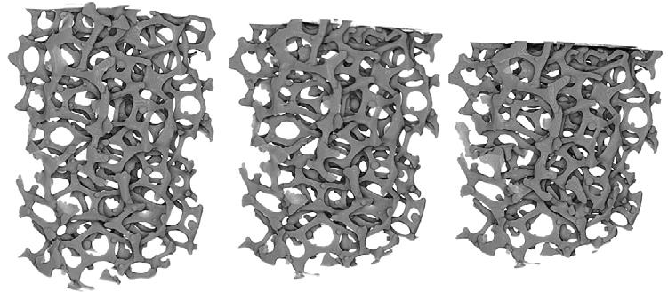
With a unique gantry-style architecture, experimental apparatus can be easily
incorporated into the X-ray chamber. These allow you to observe changes in materials under dynamic conditions such as load, temperature, flow etc. With the continuous scanning capability, you won’t miss any critical events as may be the case with time lapse. In doing so, you can replicate real life service conditions to see


how your material or components will perform in operation, thus accelerating your path to commercial success.

This technology is ideally suited to the development of advanced materials and structures as well as systems in life science and geological sciences.







INDUSTRY NEWS
32 | JUNE 2020 BACK TO CONTENTS WW W.M ATERIALSAUSTRALI A COM AU
MicroCT study of the crushing of a metal foam.
Advancing Materials and Manufacturing
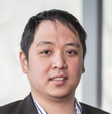

1-3 December 2021 | The University of Melbourne
Call For Papers
Closing Date: 30 July 2021
Symposia Themes
• Additive, advanced & future manufacturing, processes and
Advances in materials
Advances in steel technology
Biomaterials & nanomaterials
Ceramics, glass & refractories
Corrosion & degradation
Durable & wear resistant materials for demanding environments
Light metals design
Materials for energy generation, conversion & storage
Materials for nuclear waste forms
Materials simulation & modelling
Metal casting & thermomechanical
Nanostructured & nanoscale materials & interfaces
Innovative building materials in civil infrastructures
Photonics, sensors & optoelectronics & ferro electrics
Progress in cements & geopolymers
Surfaces, thin films & coatings



Themes
Advances in materials characterisation
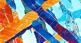
Advances in steel technology
Advanced manufacturing
Biomaterials
Cements & geopolymers
Composites in roadmaking & bridge building
Ferroelectrics
Light metals design
Translational research in polymers and composites
Use of waste materials & environmental remediation
Photos courtesy of George Vander Voort
The 7th conference of the Combined Australian Materials Societies; incorporating Materials Australia and the Australian Ceramic Society.
Davenport PETPlus IV for measuring Intrinsic Viscosity of PET Polymer
Source: Bestech Australia
PET (polyethylene terephthalate) is a commercial-grade polymer that is widely used in the manufacture of packaging, fabrics, films, and moulded parts for electronics and the automotive industry.
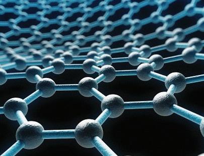
The most important characteristic that determines the quality of PET polymer is its intrinsic viscosity (IV). IV reflects the melting point of PET polymer, its crystallinity and its tensile strength. IV is dependent on the length of the polymer chain—polymer with longer chain exhibits chain entanglement behavior, which increases its intrinsic viscosity.
IV testing is important in selecting the correct grade of PET polymer for particular applications such as fibre grade, film grade or bottle grade. The testing is carried not only in the research and development stage, where new polymers and products are developed, but also across all points of the supply chain process to control product quality and optimise the operating conditions for constant production.
Polymer IV can be measured by using the solvent-free approach based on the extrusion of the polymer through a die using a specific instrument. It is
a powerful alternative to both solventbased techniques and the free blowing method as the halogenated solvent used for dissolution of the polymer is costly and hard to dispose.
The PETPlus IV testing instrument is suitable for this application. It can test polymers at all stages of the process, such as resins, powder, dry granules, molten polymer, performs, PET bottles, film and re-grounded materials. The instrument can measure the degradation factor and provide the mean and standard deviation for each batch. Once the sample is dried, the test can be initiated and completed in less than 20 minutes.
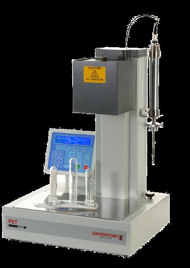
Testing the intrinsic viscosity of PET polymer is tricky as it undergoes thermal, oxidative or hydrolitic degradation during processing. The polymer degradation results in the decrease of its IV and increase the number of the carboxyl-end group. The initial degradation rate is fast due to the presence of residual water.
First, different samples of molten PET are dried under vacuum. They are then placed into a sealed barrel with a die at the base and forced through the narrow calibrated die at 295°C for 17 minutes. The barrel contains a free space that is filled
with nitrogen gas to ensure there is no degradation due to moisture. During this process, the LVDT probe movement against time is recorded and displayed.
After extrusion, the software included with the instrument performs a linear regression to obtain the polymer degradation rate and initial melt viscosity. The system then measures the optimum flow rate and calculates intrinsic viscosity.
The PETPlus -IV Test Instrument can be operated in stand-alone mode or used with the powerful data analysis software, NEXYGENPlus PET. The instrument displays trends in intrinsic viscosity measurements, thereby enabling easy comparisons between suppliers and batches with full statistical analysis and search facilities. It can also store up to 10 dry samples from the dryer for several days.
Dynamic & Fatigue testing system

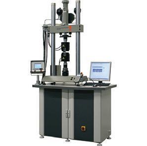
GLOBAL TECHNOLOGY LOCAL SUPPORT Email: enquiry@bestech.com.au Call: (03) 9540 5100
INDUSTRY NEWS
Ergonomic, Versatile, High Performance Testing System www.bestech.com.au Testing wide range of materials: • Advanced/ Biomedical • Manufacturing Assemblies • Dental Implants TMF, LCF, Fracture Mechanics, HCF, High-strain rate & Component testing 34 | JUNE 2020 BACK TO CONTENTS WW W.M ATERIALSAUSTRALI A COM AU
Next Generation Phenom XL G2 Desktop SEM Brings Advanced Automation to the Forefront

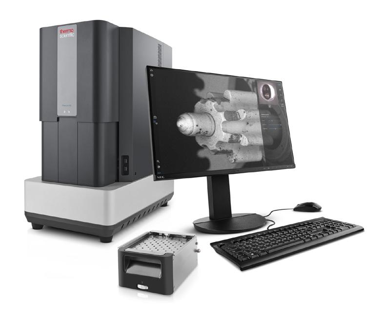
While traditional SEMs remain relatively large and difficult to operate, Thermo Scientific Phenom desktop SEMs provide an alternative that is smaller, faster and now, even easier to use.
Building on the performance of its predecessor, the next-generation Phenom XL G2 Desktop Scanning Electron Microscope (SEM) delivers new automation solutions for quality control (QC), enabling more detailed failure analyses than is possible using optical microscopes. Manual, repetitive tasks can be automated to allow a high volume of samples to be quickly processed and to discover potential failures early to guide rapid adjustment to production processes. Particles, pores, fibres or large SEM images can be automatically characterised and foreign
contaminants automatically identified and evaluated for chemical composition.
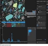
Users can obtain high-quality images in just 40 seconds—three times faster than other desktop SEM systems on the market. Offering an improved resolution of 10 nanometers, the system enables more resolving power and the ability to explore large samples of up to 100 by 100 millimeters.
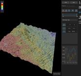
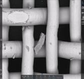
A key feature of the Phenom XL G2 is its easy-to-use, intuitive user interface combining two screens into one for viewing images and performing analysis. With one simple click on the impurity, users can see what elements are present using the live energy-dispersive X-ray (EDS) analysis. The optical navigation camera makes it possible to view the entire sample while the user is in SEM mode.
Requiring little lab space, the Phenom XL G2’s compact size allows users to place the microscope exactly where it’s needed—whether that’s in the lab or on the production line for real-time analyses. The latest Phenom ParticleX series is designed to provide technical cleanliness and additive manufacturing companies faster QC analyses of materials. Consisting of a high-performance Phenom XL Desktop SEM with automation software packages, the Phenom ParticleX provides in-house analysis and validation of produced goods against industry-approved standards, up to ten times faster than outsourcing.
For further information, contact us.
ATA Scientific Pty Ltd +61 2 9541 3500 enquiries@atascientific.com.au www.atascientific.com.au

INDUSTRY NEWS
ATA Scientific WW W.M ATERIALSAUSTRALI A COM AU BACK TO CONTENTS 35 | JUNE 2020 ATA Scientific Pty Ltd | enquiries@atascientific.com.au | www.atascientific.com.au | +61 2 954 1 3 50 0 • New 24’’ User Interface • Full screen SEM image • Magnification 200,000x • <10nm resolution • Live EDS, SED, BSD • High quality images in just 40 seconds CONTACT US FOR A QUOTE Advanced automation. Large samples upto 100 x 100 mm. Element identification using X -ray (EDS) detector Eucentric sample holder enables tilt and rotation. Long-lifetime, high brightness CeB ₆ source. ParticleMetric, PoroMetric, FiberMetric and 3D Roughness.
Source:
University of Western Australia

 Source: Sally Wood
The University of Western Australia (UWA) was the state’s first university, having been established in 1911. As the first free university in the British Empire, UWA has a history of promoting equal access to tertiary education for all. UWA has now garnered a reputation for being a leading university in Australia, with more than 24,000 students enrolled across their four faculties.
The existence of UWA is largely thanks to Sir John Winthrop Hackett, who was the proprietor and editor of The West Australian newspaper. As the founding Chancellor of UWA, he bequeathed more than £425,000, which is approximately the equivalent of $32 million in modern currency.
As such, Sir John Winthrop Hackett was able to fulfil his long-standing vision and passion to provide Western Australia with a university. Moreover, the establishment of a university helped to develop the state’s pioneering economy which, at the time – with a population of just 121,000 people – relied largely on the agricultural, mining and pastoral industries. UWA now exists across three campuses:
Crawley, Claremont and Albany, with Crawley being the primary campus located just 10 minutes away from Perth’s central business district.
UWA’s commitment to research is exemplified by their membership in the Group of Eight – the coalition of top research universities in Australia. Additionally, UWA has been recognised as one of the world’s Top 100 universities through the Academic Ranking of World Universities. As such, UWA has earnt a reputation internationally for its excellence in teaching, learning and research.
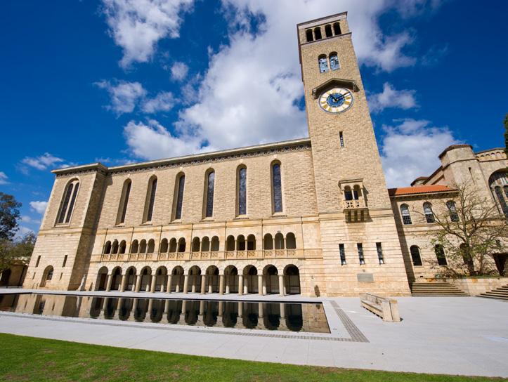
UWA’s Contribution to Materials Science and the School of Molecular Sciences
UWA’s School of Molecular Sciences contributes significantly to the materials science industry through its dedication to educating the leaders of tomorrow, as well as generating practical and translatable solutions to some of the key problems faced globally regarding chemical sciences, molecular plant sciences, health and medicine, and future materials.
Within the School of Molecular Science, research spans across several fields and disciplines, including chemistry, chemical biology, biochemistry, molecular biology,
molecular genetics, nanotechnology, molecular materials, computation, synthetic biology and systems biology. Additionally, it is home to internationally recognised, multidisciplinary research centres and groups, including the ARC Centre of Excellence in Plant Energy Biology and the Hartmann Human Lactation Research Group.
Through industry and community partnerships and collaborations, the School of Molecular Sciences is able to support high-quality, multidisciplinary research and industry engagement.
The School of Molecular Sciences is based in UWA’s Bayliss Building, which is home to a range of first-class, cutting edge facilities, including:
- Biomolecular Interactions Facility
- High Performance Computer Cluster
- Mechanical Workshop
- Protein Production and Structure Facility
- Spectroelectrochemistry
Additionally, within the Bayliss Building, the Centre for Microscopy, Characterisation and Analysis (CMCA) offers a range of world-class facilities that support the planning and application of cutting-edge techniques, as well as assisting with data interpretation. The analytical techniques that CMCA are able to facilitate include:
- Mass spectrometry
- Nuclear Magnetic Resonance (NMR) spectroscopy
- Scanning probe microscopy
- Small molecule X-ray crystallography
Current Research at the School of Molecular
Sciences
Some of the research currently being undertaken by UWA’s School of Molecular Sciences include:
UNIVERSITY SPOTLIGHT 36 | JUNE 2020 BACK TO CONTENTS WW W.M ATERIALSAUSTRALI A COM AU
- Developing novel methodology and biological applications using advanced imaging techniques
- Deciphering organelle transport mechanisms in plants
- Structure-based design of new herbicides
- Designing functional molecules and materials with supercomputers
- Insect technology as a means of converting polystyrene waste into high value protein products
- Developing new methods for detecting hormone-like signalling compounds that affect plant development
Biochemistry and Molecular Genetics Research at the School of Molecular Sciences
UWA’s School of Molecular Sciences conducts significant research in the fields of biochemistry and molecular genetics. Innovative research and strong industry collaboration have enabled the creation of new therapeutics and biotechnological tools, which play a significant role in the transformation, advancement and understanding of medicine, agriculture and evolutionary biology.
The highly interdisciplinary research conducted within the School of Biochemistry and Molecular Genetics encompasses fields such as structural biology, metabolomics, proteomics, redox regulation and signalling, RNA biology, genomics and epigenomics, synthetic
biology, plant genetics, organelle biogenesis, chemical biology, drug design, bionanotechnology, enzymology and computational biology.
Chemistry Research at the School of Molecular Sciences
Within the School of Molecular Sciences, the School of Chemistry contributes a significant amount of research in the area of materials science.
The interdisciplinary research areas that make up UWA’s School of Chemistry include biological chemistry, inorganic chemistry, materials and nanotechnology, molecular structure. Molecular synthesis and catalysis, organic chemistry and physical chemistry.

Biomaterials and Nanodentistry
UWA’s Biomaterials and Nanodentistry research program consists of a highly interdisciplinary research group that aims to translate biomaterials and nanotechnology research into clinical practices in order to provide patients with better dental treatment.
Some of their current projects include:
- Establishing a novel platform for drug delivery to dentin-pulp complex using nano-carriers
- Bioengineering of dental hard tissues for therapeutic and preventative dental applications
- The interaction of high-intensity focused
Are Laxatives the Answer to More Powerful Mobile Phones and Cars that Run Better?
A global research team including scientists from The University of Western Australian has found laxatives may hold the key to creating mobile phones that don’t need batteries to operate, and hybrid cars that run better.
The unlikely discovery came as scientists uncovered materials in laxatives that could be used to create new electrolytes and powerful capacitors (components that store electrical energy) for use in electronics.
Australian lead on the project, Professor Rob Atkin from the UWA School of Molecular Sciences, said by studying the molecular structure of laxatives the team created a detergentlike substance.
ultrasound and dental hard tissues
- 3D-printing of biomaterials scaffolds for dental repair
- Milled and 3D printed dental prosthetic appliances
Additional program objectives include:
- Enhancing the performance of toothcoloured restorative materials through chemical modification
- Investigating the potential of human dentin as a natural scaffold for osteogenic and odontogenic stem cell differentiation
“This comprises of oil and soluble parts, two materials that naturally repel each other,” Professor Atkin said.
“The oily parts cluster together and form a barrier that traps positive charged ions. As the amount of positively charged ions near the surface is very high, a much greater charge can be stored, opening up a whole new way of storing electricity.”
“Electric cars are more environmentally friendly than cars that run on petrol, but the current challenge is that they have limited ranges and long charging times, typically more than four hours.”
“However, this breakthrough could solve these problems through the development of high performance capacitors. This technology could also be used to power mobile phones, meaning faster charging times, and allowing them to run much longer between charges.”
Professor Atkin said the finding held exciting possibilities for future advancements in technology. “Not only will this create more powerful and efficient devices, but also provide great environmental benefits,” he said.
UNIVERSITY
SPOTLIGHT
WW W.M ATERIALSAUSTRALI A COM AU BACK TO CONTENTS 37 | JUNE 2020
BREAKING NEWS
Ultralight, Flexible Solar Cell Keeps Tech in Shape
An ultralight flexible solar cell, 10 times thinner than the width of a human hair, could hold the key to promising power sources for future wearable technology.
An international research team, involving Monash University, has developed a super-thin photovoltaic cell that has high efficiency, supreme mechanical bending and stretching capacity, and capabilities to provide a long-lasting power source. Researchers successfully developed novel mechanically robust photo-absorber materials that can make ultra-flexible solar cells. These cells can achieve a power conversion efficiency of 13% with 97% efficiency retention after 1,000 bending cycles, and 89% efficiency retention after 1,000 stretching cycles.
Tests have shown that when this solar cell was treated with a special method, its performance had only dropped 4.8% after a staggering 4,736 hours. It could run for more than 20,000 hours – about 2.5 years – with minimal degradation, and had an estimated shelf life of 11.5 years.
At a size of just 2cm squared – roughly the same as an Australian 5c piece – this solar cell is light enough to be supported by a flower petal and can generate 9.9 watts of power per gram.
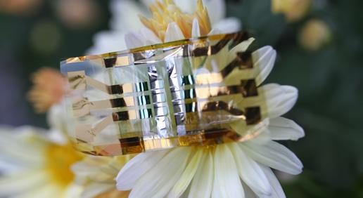
With further testing, this revolutionary device could be used as a replacement for batteries in a number of future technologies such as mobile phones, watches, internet of things (IoT), and in biosensors.
Despite its size, these low-cost solar cells can be reproduced easily with continuous printing technology, which makes them ideal for the fast tracking and mass production of wearable technology.
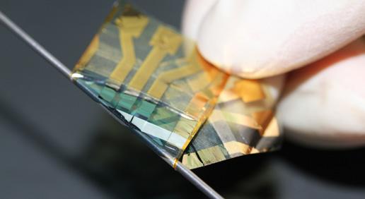
UniSA in Joint Project to Help Halt the Spread of COVID-19
In an Australian first, millions of respirator and surgical masks made by Adelaide packing company Detmold will be tested at the University of South Australia (UniSA) and Flinders University laboratories to help stop the spread of COVID-19.
The South Australian State Government is allocating $450,000 for the project where more than 20 million masks will be produced and tested each month for local and national markets.
Professor Emily Hilder, Director of UniSA’s Future Industries Institute at Mawson Lakes, where the testing will take place, said the University was excited to collaborate with Flinders University to support local testing of masks.
“This both improves our capacity to respond to the immediate demands due to COVID-19 and also provides new opportunities that will support the long-term viability of manufacturing businesses in South Australia,” Professor Hilder said.
South Australian Health Minister Wade said the testing facilities at the two universities would provide ongoing assurance to the public of the quality and safety of equipment being used in our hospitals.
“I commend the initiative of the University of South Australia and Flinders University for the important role they are playing to improve the delivery of this vital protective medical equipment to Australian health workers,” said Minister Wade.
Innovation and Skills Minister David Pisoni said the locally made medical equipment would start rolling off the production line in May. “In these unprecedented circumstances, science, research, innovation and collaboration have never been more important. With these new testing facilities at UniSA and Flinders University, we will be able to deliver this medical equipment to hospitals within weeks.”
INDUSTRY NEWS INDUSTRY NEWS
An international research team, involving Monash University, has created a flexible solar cell that could revolutionise future wearable technology.
38 | JUNE 2020 BACK TO CONTENTS WW W.M ATERIALSAUSTRALI A COM AU
Millions of respirator and surgical masks will be tested at UniSA and Flinders University laboratories to help stop the spread of COVID-19.
UQ Ventilator Design Hackathon Puts Engineers to Work
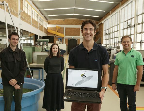
A mission to design ventilators that could serve COVID-19 patients brought together 200 bright engineers and their students at The University of Queensland (UQ).
The UQ Ventilator Design Hackathon tasked students and their mentors to design a variety of ventilator components that could be manufactured locally within an emergency time frame.
UQ’s Professor Ross McAree said the work engaged students in the broader engineering effort to significantly enhance Queensland’s capability to respond to COVID-19-related ventilator shortages.
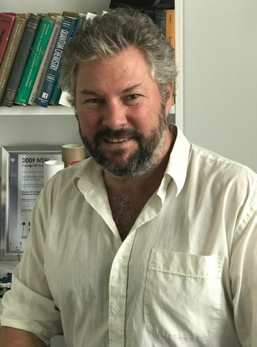
“We believe that engineering is about working in a team on real-world challenges, not just performing well in an exam,” Professor McAree said. “This is a great opportunity for our students to work with industry professionals to make a lasting impact in the community.”
Taking ventilator specifications set out by Australia’s Chief Scientist, Dr Alan Finkel, the design groups have worked with clinical advisor, Brisbane anaesthetist Dr Erich Schulz.
Electrical engineering and business student, Rohit Nunna, said the intensive week-long effort involved working remotely and, for some, at the UQ Innovate makerspace.
“It’s been a huge positive learning curve,” Nunna said. “I can now really appreciate the beauty of fundamental engineering principles and how they need to be applied to a complex problem like building a ventilator.”
Professor McAree said the hackathon would help position Queensland for longer term engineering and manufacturing security around medical devices.
“The best ventilator component designs from the hackathon will be further developed and prototyped for evaluation in Queensland hospitals,” he said.
Solving a Mystery in 126 Dimensions
One of the fundamental mysteries of chemistry has been solved by Australian scientists – and the result may have implications for future designs of solar cells, organic light-emitting diodes and other next-gen technologies.
Benzene – which comprises six carbon atoms matched with six hydrogen atoms – is the smallest molecule that can be used in the production of opto-electronic materials, which are revolutionising renewable energy and telecommunications tech. It is also a component of DNA, proteins, wood and petroleum. The mystery around the structure of the molecule arises because although it has few atomic components it exists in a state comprising not just four dimensions – like our everyday ‘big’ world – but 126.
Measuring a system that complex – and tiny – has until now proved impossible, meaning that the precise behaviour of benzene electrons could not be discovered.
Now, however, scientists led by Timothy Schmidt from the ARC Centre of Excellence in Exciton Science and the University of New South Wales (UNSW) in Sydney have succeeded in unravelling the mystery.
Professor Schmidt, with colleagues from UNSW and CSIRO’s Data61, applied a complex algorithm-based method called dynamic Voronoi Metropolis sampling (DVMS) to benzene molecules in order to map their wavefunctions across all 126 dimensions
“What we found was very surprising,” said Professor Schmidt. “The electrons with what’s known as up-spin double bonded, while those with down-spin remained single.”
“That wasn’t what we were expecting, but it could be good news for future technological applications. Essentially, it reduces the energy of the molecule, making it more stable, by getting electrons, which repel each other, out of each other’s way.”
INDUSTRY NEWS
BREAKING NEWS
L to R: Giordano Masnata, Isabelle Fleming, Mitchell Davis and Mitchell Heard.
Picture by Mark Calleja.
WW W.M ATERIALSAUSTRALI A COM AU BACK TO CONTENTS 39 | JUNE 2020
Professor Timothy Schmidt, unravelling the mystery of benzene. Credit Exciton Science.
BREAKING NEWS
Better Predictions of the Working Life of Industrial Components
A niggling disparity between an established mathematical model to predict creep crack growth behaviour in materials in high-temperature environments and actual data prompted Dr Warwick Payten to re-asses the approach and revise the model. Dr Payten is a senior research scientist in the nuclear fuel cycle group at ANSTO and one of Australia’s leading experts in determining the remaining operational life of materials in hightemperature environments.
In research published in EngineeringFractureMechanics, Payten shared a revised model to predict creep growth rates that was validated in a range of materials.
“Being able to more accurately predict crack growth in real components is highly useful because it allows you to potentially extend the life of operating industrial plants and conventional, solar and nuclear power stations with confidence,” said Payten.
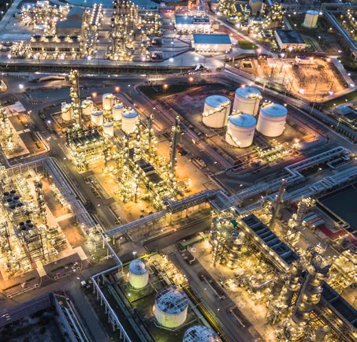
“Engineers and those of us who work in fracture mechanics have been aware for many decades that the current equations developed in the 1980s by Nikbin Smith and Webster (NSW) are overly conservative,” Payten added.
In the NSW equation to determine plane strain crack growth, which is used in all the engineering codes, you multiply the plane stress crack growth by a multiaxial factor of 30 or 50. This produces a high estimate for failure, or shorter operational life for the component.
After testing and validating the new model a range of different materials, including carbon, steels, stainless steels, inconels and superalloys, the materials used to construct current and future power reactors, Payten said he was confident the model could be used almost universally.
Payten recommends that the universal crack growth equations and the FEA code be changed to provide a more realistic prediction of component life.
Griffith 3D Print Experts Create PPE for Frontline Workers
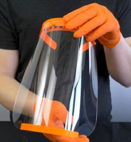
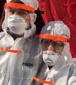
Griffith University’s expertise and 3D printers are being used to help manufacture essential protective equipment for frontline health workers across Australia.
As part of a call-out by the Queensland State Government’s health authorities, hospital-grade designs were shared with volunteers with access to 3D printers. Face shields and other personal protective equipment (PPE) are being created using 3D printers from a number of facilities and schools across the university to help maintain supplies during the COVID-19 crisis. Griffith’s Advanced Design and Prototyping Technologies Institute (ADaPT) and Queensland College of Art (QCA) design studio are among the teams that have recently swung into action, after a request for help from Metro North Hospital and Health Service.
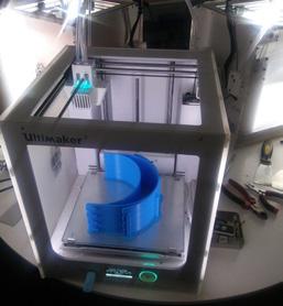
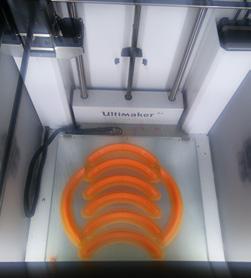
Metro North operates five hospitals on Brisbane’s northside, including Royal Brisbane and Women’s Hospital and The Prince Charles Hospital.
According to Adapt Manager Derek Smith, ADaPT was perfectly placed to respond. “ADaPT already works closely with the Gold Coast University Hospital on a range of projects, and we’ve been able to move fast to make PPE parts,” Smith said.
“We’re leading the different disciplines across the university that are working on this project, from design and engineering to health. It is fantastic to see our community rising to the challenge.”
QCA Technical Officers Chris Little and Alex Innocenti have been running several 3D printers around the clock, making hundreds of face shields. “We’re one part of a very big project worldwide, but together, we can help frontline staff in the fight against COVID-19,” Little said.
INDUSTRY NEWS INDUSTRY NEWS
40 | JUNE 2020 BACK TO CONTENTS WW W.M ATERIALSAUSTRALI A COM AU
Seeking the Sounds of Superfluids at Swinburne
A Swinburne University of Technology study published recently examines the propagation of energy as sound waves in a quantum gas, revealing for the first time strong variations in the nature of the sound wave as a function of temperature.
At low energies, this energy travels via the collective movement of many particles moving in sync – essentially, as sound waves – quantified using quasiparticles known as phonons.
Below the superfluid transition temperature (Tc) these sound waves in a unitary Fermi gas can propagate without collisions and are driven by ripples in the phase of the superfluid order parameter (wave-function)—this mode is known as the Bogoliubov-Anderson (BA) phonon.
Above Tc, the sound waves become more strongly-damped, and collisions play a dominant role:
• < Tc In the colder, superfluid mode, damping is dominated by collisions with thermally excited quasiparticles and is well described by (QRPA) theory.
• > Tc Above the transition temperature, the stronglydamped mode occurs at the crossover between collisionless hydrodynamic regimes.
• >> Tc At even higher temperatures, collective propagation of sound-wave vanishes, and excitation is dominated by the energy of individual particles.
Strong similarities were identified in the temperature dependence of sound in the unitary Fermi gas and the behaviour of phonons in liquid helium, which was one of the first superfluids identified historically.
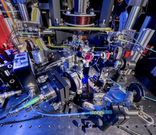
The study of many-body quantum systems with strong interparticle interactions is of great interest for the understanding of novel materials. The study also provides quantitative benchmarks for dynamical theories of strongly-correlated fermions.
Graphene Solar Heating Film Offers New Opportunity for Efficient Thermal Energy Harvesting
Researchers at Swinburne’s Centre for Translational Atomaterials have developed a highly efficient solar absorbing film that absorbs sunlight with minimal heat loss and rapidly heats up to 83°C in an open environment.
The graphene metamaterial film has great potential for use in solar thermal energy harvesting and conversion, thermophotovoltaics (directly converting heat to electricity), solar seawater desalination, wastewater treatment, light emitters and photodetectors.
The researchers have developed a prototype to demonstrate the photo-thermal performance and thermal stability of the film. They have also proposed a scalable and low-cost manufacturing strategy to produce this graphene metamaterial film for practical applications.
“In our previous work, we demonstrated a 90 nm graphene metamaterial heat-absorbing film,” said Professor Baohua Jia, founding Director of the Centre for Translational Atomaterials.
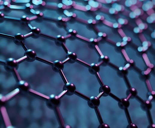
“In this new work, we reduced the film thickness to 30 nm and improved the performance by minimising heat loss. This work forms an exciting pillar in our atomaterial research.”
Lead author Dr Keng-Te Lin said, “Our cost-effective and scalable structured graphene metamaterial selective absorber is promising for energy harvesting and conversion applications. Using our film an impressive solar to vapour efficiency of 96.2% can be achieved, which is very competitive for clean water generation using renewable energy source.”
Co-author Dr Han Lin added, “In addition to the long lifetime of the proposed graphene metamaterial, the solar-thermal performance is very stable under working conditions, making it attractive for industrial use. The 30 nm thickness significantly reduced the amount of the graphene materials, thus the costs, making it accessible for real life applications.”
INDUSTRY NEWS
WW W.M ATERIALSAUSTRALI A COM AU BACK TO CONTENTS 41 | JUNE 2020
BREAKING NEWS
Ultracold atomic lab at Swinburne University of Technology.
Researchers at Swinburne’s Centre for Translational Atomaterials have developed a highly efficient solar absorbing film.
BREAKING NEWS
Self-Reinforcing Material Responds to External Force
Materials with adaptable properties, like those of wood and bone, can provide safer structures, save money and resources, and reduce their environmental impact, claim the team at Johns Hopkins University.
“Imagine a bone implant or a bridge that can self-reinforce where a high force is applied without inspection and maintenance. It will allow safer implants and bridges with minimal complication, cost and downtime,” said Sung Hoon Kang, an assistant professor in the Department of Mechanical Engineering, Hopkins Extreme Materials Institute, and Institute for NanoBioTechnology at Johns Hopkins University.
Bones use cell signals to control the addition or removal of minerals taken from blood around them. Inspired by these natural materials, Kang and colleagues sought to create a materials system that could add minerals in response to applied stress.
The team started with materials that convert mechanical forces into electrical charges as scaffolds that can create charges proportional to external force placed on it. The team’s hope was that these charges could serve as signals for the materials to start mineralisation from mineral ions in the environment.
Kang and colleagues immersed polymer films of these materials in a simulated body fluid mimicking ionic concentrations of human blood plasma. After the materials incubated in the simulated body fluid, minerals started forming on the surfaces. The team found they could control the types of minerals formed by controlling the fluid’s ion composition.
Kang hopes that these materials can someday be used as scaffolds to accelerate treatment of bone-related disease or fracture, smart resins for dental treatments or other similar applications.
3Q: Robert Macfarlane on Cleaning Your Smartphone Screen
To help curb the spread of the COVID-19 virus, public health experts have emphasised the need for cleaning and disinfecting frequently touched surfaces. But what about our smartphones and other personal electronic devices that we touch throughout the day?
Many smartphone manufacturers advise against using cleaning products or disinfectants to clean touchscreens. Robert Macfarlane, the Paul M. Cook Assistant Professor in Materials Science and Engineering at MIT, is developing new techniques to manufacture materials via self-assembly that could eventually be used to create protective coatings, adhesives, sensors, and other types of devices.
Macfarlane explained that placing an ‘oleophobic’ coating on a surface — a material that does not have a strong affinity for binding to oily substances — minimises the amount of oils that are left behind.
Oleophobic coatings are commonly made of fluorinated polymers or fluorocarbons, which are classes of molecules that do not really have strong binding affinity for either water-soluble or oil-soluble materials. While using rubbing alcohol or an alcohol-based wipe is unlikely to remove this coating entirely, prolonged exposure to alcohols in high concentration could potentially disrupt this coating by either removing small patches of the fluorocarbons or altering the coating’s distribution so that it is not entirely uniform across a surface.
“The oleophobic coatings that we already use are not entirely impossible to clean, and they probably already prevent microbial adhesion at least to a limited degree. However, they don’t completely eliminate the possibility of contamination, which is something we are now thinking about a lot more given the current pandemic,” Macfarlane explained.
Team of Canadian and Italian Researchers Breaking New Ground in Materials Science
A study by a team of researchers from Canada and Italy recently published in Nature Materials could usher in a revolutionary development in materials science, leading to big changes in the way companies create modern electronics. The goal was to develop two-dimensional materials, which are a single atomic layer thick, with added functionality to extend the revolutionary developments in materials science that started with the discovery of graphene in 2004.
These results will foster more studies on a wide range of two-dimensional conjugated polymers with different lattice symmetries, thereby gaining further insights into the structure versus properties of these systems. The Italian and Canadian team demonstrated the synthesis of large-scale two-dimensional conjugated polymers, also thoroughly characterising their electronic properties. They achieved success by combining the complementary expertise of organic chemists and surface scientists.
INDUSTRY NEWS INDUSTRY NEWS
42 | JUNE 2020 BACK TO CONTENTS WW W.M ATERIALSAUSTRALI A COM AU
Professor Rob MacFarlane studies materials science and engineering at MIT. Image credit: Lillie Paquette, MIT School of Engineering.
New Recyclable Material Could Revolutionise Construction Industry
A global research team, headed by Monash University, is pioneering a breakthrough recyclable material that could revolutionise the construction industry, assist disaster-affected areas, and become used in space exploration.
Researchers are leading the development of archimats – an emerging area of ‘architectured’ materials that have an organised intertwined or interlocked inner architecture. As a result, archimats have an extra degree of freedom expanding the design space that conventional composite materials, such as concrete, cannot possess.
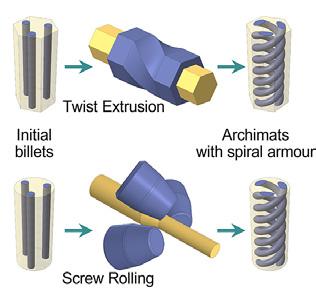
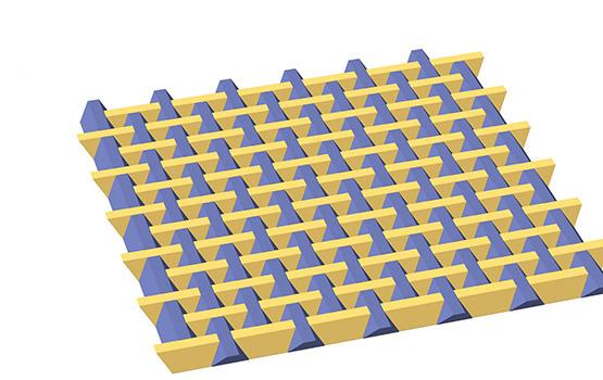
Archimats can be engineered to have superior strength, enhanced ductility, a high tolerance to damage, good thermal insulation and sound absorption. They can also better absorb energy, as well as provide improved compliance and flexibility.
One way to achieve this superior property profile, especially of metallic materials, is through severe plastic deformation (SPD) – a special metalworking technique that results in an ultrafine grain size or nanocrystalline structure. The structural patterns caused by SPD processing can improve the mechanical characteristics and physical properties of materials.
With the potential to revolutionise the construction, materials and production industries, archimats can be used:
• In the construction industry to reduce the use of concrete and cut carbon dioxide emissions associated with its production;
• To build or rebuild in arid or disaster-affected zones. This includes rapidly deployable and removable structures in danger areas, such as a town or city impacted by fire, for first responders and displaced citizens;
• In extra-terrestrial and space construction. The European Space Agency is already considering this type of architectured material for the construction of a lunar base; and
• In smart toys and games, such as 2D and 3D puzzles.
Interfaces the Key in Atomically-Thin, ‘High Temperature’ Superconductors
An international FLEET collaboration publishing a review of atomically-thin ‘high temperature’ superconductors finds that each has a common driving mechanism: interfaces.
The team, including researchers from the University of Wollongong, Monash University and Tsinghua University (Beijing), found that interfaces between materials were the key to superconductivity in all systems examined.
The enhancement of superconductivity at interfaces (interface superconductivity enhancement effect) in atomically-thin superconductors is a unique tool for discovering new hightemperature superconductors, and could be used to finally unlock the elusive mechanism behind high-temperature superconductivity.
Systems studied include:
• Elemental metals grown on semiconductors
• Single-layer iron-based superconductors
• Atomically-thin cuprate (copper based) superconductors
The review investigated the role of molecular-beam epitaxy (MBE), scanning tunnelling spectroscopy (STM/STS), scanning transmission electron microscopy (STEM), physical properties measurement system (PPMS), in fabricating and identifying atomically-thin superconductors.
Breakthrough in Energy Storage Set to Drive a Cleaner Future
Deakin’s Institute for Frontier Materials researchers, in collaboration with researchers from the University of Western Australia and Monash University, have discovered that super concentrated ionic liquids are key to achieving better batteries for future use.
The new work by ARC Centre of Excellence for Electromaterials Science (ACES) PhD student, Dmitrii Rakov and co-led by Professor Maria Forsyth and Dr Fangfang Chen presents an important breakthrough in the field, paving the way for the next generation of high energy density batteries for use in households and industries worldwide.
Professor Forsyth said this breakthrough is a key to achieving a clean energy future. “This finding is very significant because it explains for the first time why an ideal combination of sodium metal anode and safe, high performing ionic liquid electrolytes can lead to much better batteries all round.”
“Using molecular simulations coupled with experimental design, this is the first time we’ve been able to explain this optimised behaviour. Society is craving increased battery life, energy density and safety for state of the art Lithium ion batteries that can be used in energy storage for applications such as powering transportation and clean energy for homes,” Professor Forsyth said.
Current worldwide progress has been constrained by the type of electrolytes commonly used to make batteries. While their work has demonstrated the mechanism for sodium metal batteries, the team said the findings are applicable to other advanced batteries including lithium and zinc metal batteries.
INDUSTRY NEWS INDUSTRY NEWS
WW W.M ATERIALSAUSTRALI A COM AU BACK TO CONTENTS 43 | JUNE 2020
BREAKING NEWS
Mortarless construction: rapidly deployable pavements composed of interlocked tetrahedronshaped blocks made from different materials. Image courtesy of Monash University.
Employing the SPD processes of twist extrusion and screw rolling to produce archimats with spiral armour. Image courtesy of Monash University.
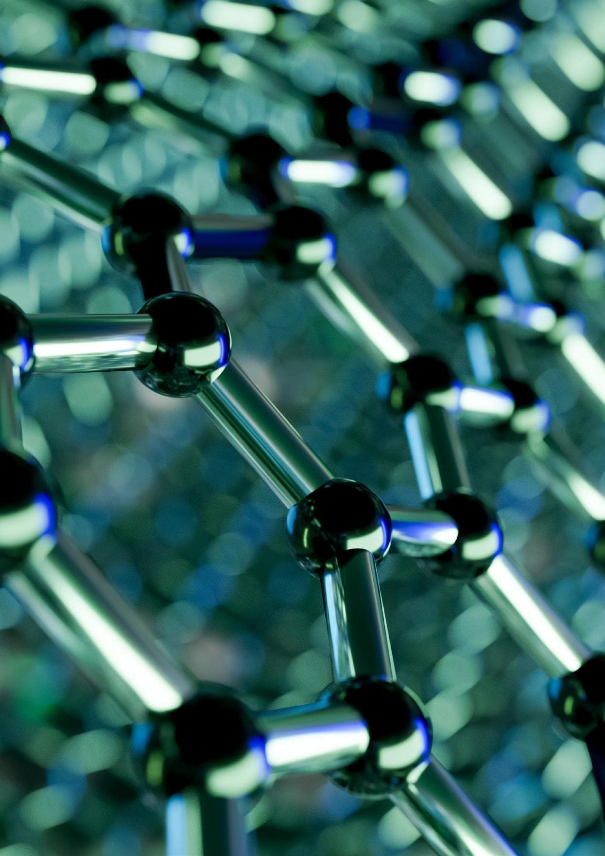
technology and
at
FEATURE – Nanotechnology 44 | JUNE 2020 BACK TO CONTENTS WW W.M ATERIALSAUSTRALI A COM AU
Nanotechnology Revolutionising
industry
an atomic scale.
Nanotechnology broadly refers to the understanding and control of the physical, chemical and biological properties of matter at the nanoscale, at the dimensions between approximately one and 100 nanometres.
When observed at a nanoscale, gases, liquids and solids can exhibit physical, chemical and biological properties and behaviours that vastly differ to bulk matter. For example, some nanostructured materials may have different magnetic properties, be stronger or reflect light differently than the same material at other sizes or in other forms.
Nanotechnology is an inherently multi-disciplinary field and draws together researchers from a variety of fields. It is studied and employed across a wide range of disciplines, including physics, chemistry, biology, materials sciences, and almost all engineering disciplines.
Nanotechnology employs the physical, chemical and biological understanding of the properties of materials on an atomic and near-atomic scale to create materials and functional systems with novel and unique capabilities and properties. As such, nanotechnology is often viewed as an extension of previously existing scientific fields, recasting them into the nanoscale.
When studying nanotechnology there are two primary approaches. The first is a ‘bottom up’ approach, whereby materials and devices are designed and built from molecular components which assemble themselves chemically according to principles of molecular recognition. The second ‘top down’ approach occurs when larger entities are used to construct nanoobjects without atomic-level control.
Nanotechnology has already had a profound impact upon myriad industries globally, particularly in sectors such as electronics, computing, communications, defence, energy, biomedicine, transport and manufacturing. As understanding of nanotechnology continues to develop, so too does its applications.
food safety, manufacturing and environmental science. One of the greatest benefits that nanotechnology offers is that it is able to enhance or unleash properties of materials which enable them to be used in innovative and novel ways. For example, nanotechnology can be used to make materials stronger, lighter, more durable, more reactive, or better at conducting electricity. As such, many commercial products rely on nanotechnology to be able to perform their function.
Nanotechnology is used in a variety of both every day and sector-specific materials and processes, including:
- Nanoscale additives are added to the surface treatments of some fabrics in order to help the resist staining, wrinkling or bacterial growth, or to provide lightweight ballistic energy deflection to personal body armour.
- Nanoscale films, which are completely transparent, can be added to camera and computer displays, windows, eye glasses and other surfaces, making them water-resistant or water-repellent, antireflective, self-cleaning, anti-fog, scratch resistant, ultraviolet and infrared light resistant, antimicrobial, or electrically conductive.
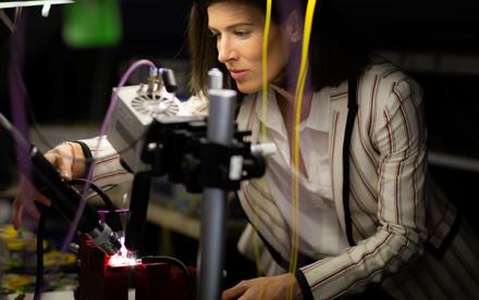
- Nanotechnology is being used to make a wide variety of products and materials more lightweight. By adding nanoscale composite polymers to items such as baseball bats, motorcycle helmets, bicycles, tennis rackets, luggage and automobile parts are able to be made lighter, stiffer, more durable and more resilient. When used for cars, airplanes, trucks, boats and space craft, nanotechnology offers the possibility of significant fuel savings.
Benefits and Applications of Nanotechnology
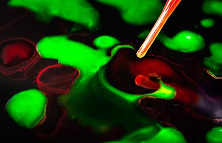
Nanotechnology offers a range of fields and disciplines a variety of benefits. It has already been able to improve and, in some cases, revolutionise technology and industry sectors. Just some of the fields that have benefited from nanotechnology include information technology, security, medicine, transportation, energy,
- Nanotechnology can help to significantly extend the lifetime moving parts necessary for the function of power tools, industrial machines and much more. This is because nanostructured ceramic coatings are much tougher than other types of wear-resistant coatings for machine parts. Furthermore, lubricants made with nanotechnology and engine oils can greatly reduce machinery wear and tear.
- Nanotechnology has been incorporated into many personal care products and cosmetics to improve their performance. For example, nanoscale titanium dioxide and zinc oxide are used in sunscreen to protect skin cells from ultraviolet radiation while appearing invisible.
FEATURE –
Nanotechnology
BACK TO CONTENTS 45 | JUNE 2020
A History of Nanotechnology
While nanotechnology is often perceived to be a recently developed field, early examples of nanotechnology exist as early as the 4th century. Though comparatively crude compared to our modern understanding of nanotechnologies, these early examples often used high heat to produce materials and objects with novel properties.
From the 6th to 15th centuries, stained glass windows were incredibly popular in European cathedrals. Their rich colours were able to be achieved with nanoparticles of gold chloride and other metal oxides and chlorides.
From the 13th to 18th centuries, Damascus steel, which was used for forging blades and swords, contained carbon nanotubes and cementite nanowires. These blades were known for their strength, resilience and ability to hold a keen edge.
More recently, a significant development in the realm of nanotechnology occurred in 1938 when Edward Müller invented the field emissions microscope at the Siemens Research Laboratory. This discovery enabled the near-atomic resolution of materials. Müller again greatly contributed to the field of nanotechnology in 1951 with the development of the field ion microscope, which provided the means to image the
arrangement of atoms at the surface of a sharp metal tip.
In 1959, Richard Feynman gave a seminal lecture at the Californian Institute of Technology. This lecture, titled ‘There’s Plenty of Room at the Bottom’ is widely regarded to be the first on the topic of technology and engineering at the atomic scale.
It wasn’t until 1974, however, that the term ‘nanotechnology’ was coined by Professor Norio Taniguchi from Tokyo Science University, who used it to describe the precision machining of materials to within atomic-scale dimensional tolerances.
In 1981, the scanning tunnelling microscope was invented by Gerd Binning and Heinrich Rohrer, which allowed scientists, for the first time, to ‘see’ individual atoms. Gerd Binning, with the help of Calvin Quate and Christoph Gerber, went on to invent the atomic force microscope in 1986, which enabled scientists to view, capture and manipulate materials down to fractions of a nanometre in size. This included the measurement of forces that are intrinsic to nanomaterials.
The 1990s saw the expansion and widespread development of nanotechnologies as early nanotechnology companies, such as Nanophase Technologies and Helix Energy Solutions Group, began to operate.
Since their inception, nanotechnologies have come a long way with significant developments and discoveries regularly being made. As nanotechnology research continues, the applications and benefits of nanotechnologies will continue to be uncovered, which will undoubtedly prove useful across a variety of industry sectors.
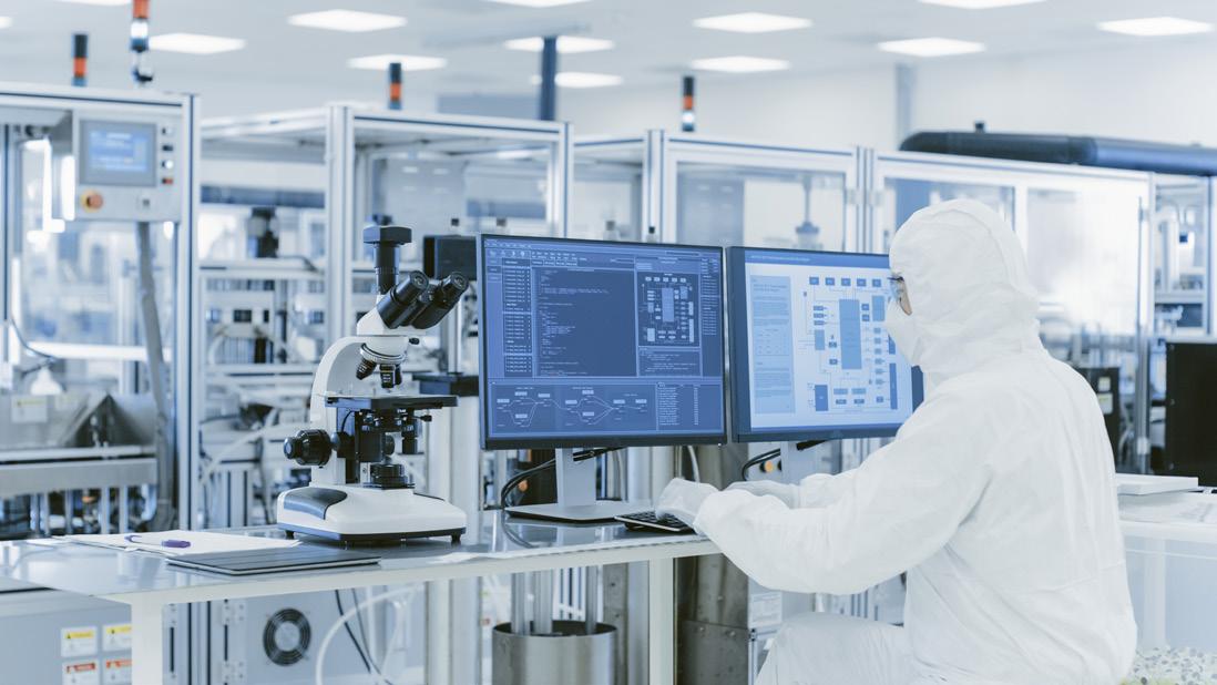
Nanotechnology Research Overview
Technological advancements across various fields over the past few decades have provided the tools necessary to undertake research at the nanoscale. Nanotechnology research is, by its very nature, inherently multidisciplinary. In order for the full potential of nanotechnology to be unveiled, it is necessary that researchers from varying fields cross traditional boundaries and are brought together to collaborate.
Since the 1990s, nanotechnology has developed as a strong research field. This is because researchers, funding bodies, regulators and governments alike have recognised the potential nanotechnology has to revolutionise multiple industries, from computers to medicine.
Nanotechnology research is necessary for the commercial integration and implementation of nanotechnology, which can ultimately offer myriad social, economic and environmental benefits.
FEATURE – Nanotechnology 46 | JUNE 2020 BACK TO CONTENTS WW W.M ATERIALSAUSTRALI A COM AU
Nanotechnology Research in Australia
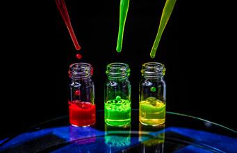
University of Queensland
In 2003, the University of Queensland established their Nanomaterials Centre in order to focus on the emerging field of nanomaterials research. Since its inception, the Centre has evolved and grown to become a large, multi-disciplinary group. Currently, the research centre’s focus is primarily in the area of the synthesis and characterisation of nanomaterials in the key areas of environment, energy, and health.
Nanomaterials offer the potential to provide the solution to many environmental issues, which is why the current environmental research being undertaken at the Centre is focused on the conversion of biofuels and chemicals, and applications in agriculture and veterinary science. In particular, nanoparticles can be used for crop modification and virus protection, which can help to improve crop protection and production. Moreover, nanoparticles can improve animal health through vaccination as well as improving the efficiency of herbicide use.
The Centre is also undertaking research regarding the potential for nanomaterials in the field of clean energy generation, storage and applications. This is a particularly pertinent field of research given that climate change and the dwindling sources of fossil fuels are some of the most pressing challenges that society currently faces.
Regarding nanomaterial research in the area of clean energy, the Centre has three main focuses: energy storage, solar cell,
and photocatalysis. In particular, the Centre’s research aims to develop nanomaterials for rechargeable batteries with high performance, long-term stability and low cost. The Centre is also exploring the potential applications of nanotechnology in commercial products, particularly in integrated electronic devices. Finally, the Centre focuses nanomaterial research efforts in the area of health care for the development of novel biomedical technologies, for drug, protein and gene delivery, as well as materials for biosensing.
complex behaviour that emerges from micromechanical interactions of soft materials such as polymer molecules, protein filaments or bilayer membranes, with a fluid environment.
Within the department of Chemical Engineering, nanomaterials research focuses on the ability to synthesise, characterise and control the nanoscale structure of materials. This has the potential to revolutionise traditional fields of chemical engineering by moving process considerations from a macroscale to one that considers that the molecular and nanoscale interaction is an intrinsic part of the design. Nanomaterials are employed by researchers in the department of Chemical Engineering for a wide variety of applications, including corrosion mitigation, water purification, catalysis, sensors, drug and gene delivery, smart coatings, functional food, theranostics, gas separation, and material composites.
University of Queensland (UQ) researchers set a world record for the conversion of solar energy to electricity via the use of tiny nanoparticles called ‘quantum dots’, which pass electrons between one another and generate electrical current when exposed to solar energy in a solar cell device.
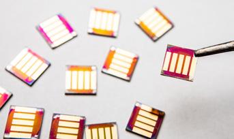
Monash University
Monash University conducts a vast amount of research in the field of nanotechnology and nanomaterials across multiple departments. Within these departments, nanotechnology and nanomaterials research is wide and varied.
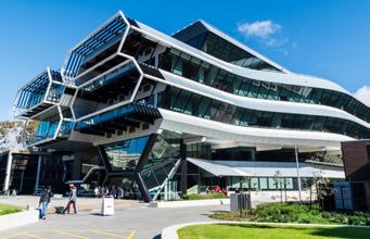
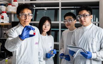
Within the department of Mechanical and Aerospace Engineering, micro and nanoengineering research covers a diverse array of areas, including the mechanisms of microswimmers, microfabricated devices for handling cell, optical sensors, and graphene supercapacitators.
Within this department, Dr Victor Cadarso Busto is undertaking research in the development of novel and scalable technologies for the fabrication of functional surfaces and 3D complex structures for a variety of applications, including optical MEMS, biomedical devices, environmental monitoring and sensing platforms.
Professor Adrian Neild is researching microfluids and microsensors for applications in biomedical devices and instrumentation. Additionally, research undertaken by Dr Prabhakar Ranganathan uses modelling and computation to study
Within the department of Materials Science and Engineering, nanostructured materials is a key area of research within the research theme of Functional and Energy Materials. In particular, areas of expertise include catalysts, sensor materials, nanostructured devices and fabrication, nanoparticles and nanocomposites, and nanostructured magnetic materials.
Australian National University
At the Australian National University (ANU) nanotechnology and nanomaterials research is conducted across several fields and departments.
Within the Materials Engineering department, fundamental and applied research is being undertaken on the development of unique synthesis techniques and novel applications of nanomaterials. This research into the applications of advanced nanomaterials is wide-ranging and includes catalysts, renewable energy and energy storage, biomedical materials, pollutant removal, and medical imaging and diagnostics.
FEATURE –
Nanotechnology
Monash University’s Engineering building at their Clayton campus.
WW W.M ATERIALSAUSTRALI A COM AU BACK TO CONTENTS 47 | JUNE 2020
They aim to create innovative nano applications that are sustainable at all life cycle stages, such as manufacturing, recycling and disposal processes. One of their main strengths is the commercialisation of applications to deliver technological innovations to the public. This is thanks to their experts who have first-hand experience in translating nanotechnology from the laboratory to industrial-scale manufacture. Within the Fabrication Engineering department, research is being undertaken in the creation of smart micro and nanoelectro-mechanical systems (MEMS and NEMS). This is done through the integration of tiny devices, which can enable many additional functionalities, from computing, sensing and communications, to energy harvesting.
Through multidisciplinary research that combines materials science, chemistry and biomedical science, ANU’s research addresses the fields of MEMS and NEMS, nanomanufacturing, energy harvesting and biomedical sensing. Specific research topics include high-throughput nanomanufacturing technology, novel NEMS-based biomedical devices, nonlinearity engineering for NEMS, high-efficiency nanostructured thin-film solar cells, and NEMS with new twodimensional nanomaterials.
One of the significant developments achieved by ANU scientists in the field of nanotechnology has been the design of ultra-small optical sensors that offer the potential to develop wearable devices that will allow doctors to medically detect and diagnose health problems and diseases, such as diabetes, much earlier than is currently possible.
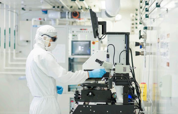
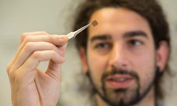
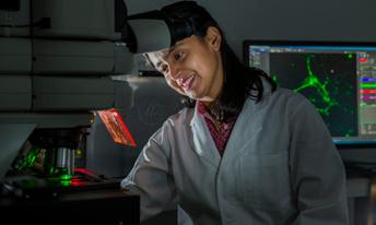
Swinburne University
Swinburne University is home to the Nanofabrication Laboratory (or Nano Lab), which facilitates research and education in nanotechnology, and is the first laboratory in the world to combine two complementary techniques that have the potential to enable two- and three-dimensional fabrication and modification of nanoparticles.
Researchers and collaborators at the Nano Lab explore a wide range of phenomena, including light propagation, absorption and scattering by nanoparticles and nanostructures, and the efficiency of nanofabrication. Specifically, areas of research include solar cells, light harvesting,
and fabrication of surfaces for photo-catalytic application.
Research undertaken at the Nano Lab has already led to significant outcomes, including: the mass production of sensors that can be used for the detection of Alzheimer’s bio-markers; development of black silicon – nano spikey surfaces of silicon – which has a bactericidal effect and has biomedical applications; and the creation of unique and novel nanomaterials using ultra-short laser pulses.
Currently, the Nano Lab is exploring 3D printing of bio-scaffolds using ultra-fast laser fabrication and using laser fabrication nanoparticles for sensing. This research offers nanomedicine a vast amount of potential.
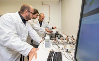
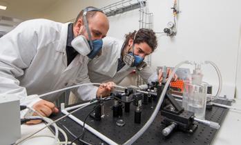
Additionally, Swinburne Optics and Laser Laboratories (SOLL) is home to the Microfabrication Facility, which is used for the preparation of samples, the deposition of dielectric and metal films, and the analysis of surface morphology and texture. The centre’s activity primarily focuses on the preparation and characterisation of nanomagnetic thin films for atom optics, and consulting work involving the preparation and characterisation techniques of various thin films, metals, and bio-materials.
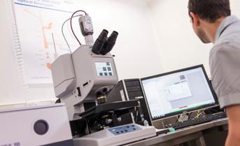
FEATURE – Nanotechnology
Dr Vini Gautam from the Research School of Engineering at ANU. Image credit: Stuart Hay, ANU.
Zelio Fusco Image credit: Lannon Harley, ANU.
Dr Mohsen Rahmani and Zelio Fusco. Image credit: Lannon Harley, ANU.
Dr Mohsen Rahmani, Zelio Fusco, and Associate Professor Antonio Tricoli. Image credit: Lannon Harley, ANU.
48 | JUNE 2020 BACK TO CONTENTS WW W.M ATERIALSAUSTRALI A COM AU
Swinburne University’s Nanofabrication Lab.
Deakin University
Deakin University is home to the Institute for Frontier Materials (IFM). One of IFM’s key strengths and research areas is in the development of novel micro and nanomaterials in order to address major challenges in the areas of energy storage, environmental protection, and health and medicine.
A significant development made by IFM researchers was their commercialisation of boron nitride nanotubes, which is a material that has excellent mechanical performance and thermal conductivity. This research has significant environmental applications, including for water resource protection by removing solvents, dyes and other contaminants.
Furthermore, IFM’s development of micro and nano-porous membrane materials has the potential to help address future environmental and biomedical challenges. Through research that focuses on the fabrication and characterisation of membranes with unique micro and nanostructures and surface properties, developments can be made in areas such as biological purification, gas separation and water treatment.
The TERI Deakin Nanobiotechnology Centre (TDNBC), which was established in 2010, is a collaboration between Deakin University and India’s The Energy and Resources Institute (TERI). Research conducted at TDNBC uses Deakin’s expertise in nanotechnology deals with food security issues in increasingly changing climates, remediation of polluted environments through natural products, improving health through novel molecules, and improving the quality of life for poor communities. TDNBC aims to achieve sustainable agricultural practices, produce safe nanodelivery systems and affordable diagnostics for agriculture and human health, mitigate environment-related problems, and develop cleaner energy.
One example of the flagship activities undertaken by TDNBC is in agriculture technology. Research is being undertaken in the areas of future biopharmaceutical formulations, pathogen and plant disease diagnostics, biological seed coating, biotic stress, and post-harvest management.
IFM researchers have found a way to extract silicon from discarded solar panels and repurpose it into nano-silicon for batteries. Working with a local company, they recover the silicon from waste solar panels and
then nano-size it, ready for use in lithiumion batteries. This is key to repurposing discarded solar cells and will prevent high-value waste going to landfill. The project has received a $150,000 grant from Sustainability Victoria, working with local company Delaminating Resources.
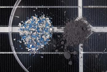
Breakthrough deals with overheating in electronic devices
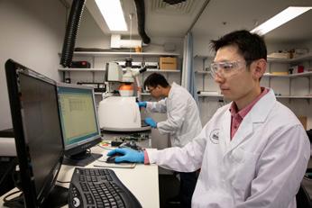
IFM researchers have made a breakthrough discovery in the area of thermal conductivity and heat regulation, which will pave the way for the next generation of foldable phones, wearable technology and miniaturised electronics.
Dr Luhua Li and Dr Qiran Cai partnered with researchers from Northern Ireland and Japan to pioneer development of a highly thermally conductive and chemically stable material to help deal with overheating issues in modern devices.
Heat management is a critical issue in miniaturised modern devices and most people will have experienced devices overheating, such as when a phone gets hot or a laptop’s internal fan starts whirring madly.
With emerging technology such as foldable phones, micro-machines and wearable devices, thermal cooling has become critical for the performance, reliability, longevity, and safety of various products.
Scientists are striving to come up with alternatives to aluminium and copper, which are conductive and potentially cause short circuit problems. Electrically insulating materials such as diamond and boron arsenide have been shown to work, but they are too rigid and inflexible, as well as too expensive for mainstream use.
By taking a chemical compound known as boron nitride (BN) and shaving it down to an atomically-thin level, the researchers were able to give the material the desired flexibility while dramatically increasing its thermal conductivity and cooling capabilities.
Atomically thin BN has better thermal conductivity than most semiconductors and insulators, along with low density, outstanding strength, high flexibility and stretchability, good stability, and excellent impermeability, making it a promising material for heat dissipation in next generation devices.
This is a fundamental breakthrough, and with time and further research it will help to open up the boundaries of what’s possible in electronic devices – particularly as the trend in next generation electronics will most likely need to be flexible.
Highlightpublication:Highthermalconductivityofhigh-qualitymonolayerboronnitrideanditsthermalexpansion.Q.Cai,D. Scullion,W.Gan,A.Falin,S.Zhang,K.Watanabe,T.Tanaguchi,Y.Chen,E.SantosandL.Li.ScienceAdvances5(6),eaav0129.
FEATURE – Nanotechnology
WW W.M ATERIALSAUSTRALI A COM AU BACK TO CONTENTS 49 | JUNE 2020
Dr Qiran Cai (L) and Dr Luhua Li discovered that atomically thin boron nitride had a very high thermal conductivity which could help cool electronics for optimum performance.
Queensland University of Technology
At the Queensland University of Technology (QUT) research is being undertaken by the Molecular Recognition and Sensors team in the development and application of nanotechnology for identification and quantification of selected analytes. The three primary research themes currently being investigated are Nanosensors and Molecular Diagnostics, Environmental and Nanoanayltics, and Light and Nanoplasmonics.
Research regarding Nanosensors and Molecular Diagnostics is primarily concerned with the design and manufacture of nanosensors and their application in diagnostic, medical and other fields. Projects under this theme include:
- Constructing chiral sensors for rapid detection and enantiomeric analysis of illicit drugs
- Next generation biomedical sensors
- Novel nanoscale platforms for the isolation and ultra-trace detection of bioactive molecules
- Functionalised RNA aptamer nanoparticles for ultra-trace detection of target analytes in biological samples via SurfaceEnhanced Raman Spectroscopy (SERS)
- Rapid detection and differentiation of Erythropoietin (EPO) isoforms in blood by handheld Raman and electrochemical devices
- Development of a Point Of Care (POC) test system for the quantification of amino acids in medical conditions
- Novel nanoformulations and nanosensors for lung delivery and molecular diagnosis of antibiotics and protein therapies
The theme of Environmental and Nanoanalytics researches the application of nanosensing technologies in an environmental monitoring context. Projects under this theme include:
- Cost effective direct osmosis system for water desalination in gas mining
- Ultra-trace detection of environmental toxicants using nanosensors
- Synthesis and application of novel fluorescent probes for the rapid spectroscopic detection of metal ions and bioactive molecules
Finally, the theme of Light and Nanoplasmonics aims to design and establish optical assemblies, and fabricate nanostructured materials that allow a
diverse array of light-material interactions to be investigated.
University of New South Wales
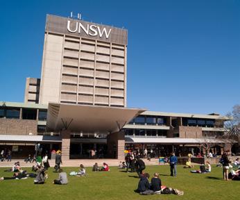
The University of New South Wales (UNSW) undertakes extensive research in the field of cancer nanotechnology. By working at the interface of chemistry and physics, researchers at UNSW are able to pioneer novel approaches to targeted and triggered therapeutics and cancer-specific imaging. Using nanomaterials that are built from clinically approved components, integration into clinical practice is enabled.
Furthermore, the co-director of UNSW Sydney’s Centre for Healthy Brain Ageing (CHeBA), Professor Perminder Sachdev AM, has undertaken significant research in the field of using nanotechnology for dementia diagnosis and treatment. Professor Sadchev proposes that nanoparticles be used to move across the blood brain barrier to target dementia-specific molecules in the brain.
Scientia Fellow, Dr Rona Chandrawati’s research focuses on the development of nantechnology sensors with colourimetric detection, which would be particularly pertinent in the areas of food and health. In particular, Dr Chandrawti’s hopes to develop technology which will enable the early detection of health issues. Additionally, they aim to develop technology which will indicate whether food is still safe to be consumed.
Additionally, UNSW researchers have developed a method that accurately measures DNA nanostructures, and discovered how to fold these materials into different shapes. This has the potential to provide technological improvements by improving resolution, speed and precision of machines and tools.
University of Western Australia
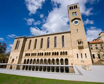
One of the primary areas of nanotechnology at the University of Western Australia (UWA) is in biomaterials and nano-dentistry. This research aims to translate biomaterials and
nanotechnology research to clinical dentistry in order to provide superior dental treatment to patients.
Currently, research is focused on drug delivery to dental tissues through nanocarriers for preventative and restorative therapies, bioengineering dental hard tissues, the interaction of high intensity focused ultrasound with tooth structure, and 3D bio-printing for the repair of dental tissues.
Current and proposed biomaterials and nano-dentistry projects include:
- Drug delivery to dentin-pulp complex using nanocarriers
- Bioengineering of dental hard tissues for the therapeutic and preventative dental applications
- The interaction of HIFU and dental hard tissues
- 3D printing of biomaterials scaffolds for dental tissues repair
- Milled and 3D printed dental prosthetic appliances
Furthermore, UWA is using nanotechnology in their research into the prevention, diagnosis and treatment of disease. In particular, they are conducting research into the commercialising of nanoparticle technology for drug delivery applications, which has the potential to enable the precise delivery of drugs to diseased cells for the treatment of cancer and other diseases through ‘loaded’ nanoparticles. UWA research is also employing nanotechnology to develop novel methodology and biological applications. The potential for this research includes the development of a multimodal and multiscale bioimaging platform based on complementary techniques, as well as developing an understanding of biological processes, such as molecular mechanisms of lipid transport, action mechanisms of pharmaceutical compounds, and the toxicology of nanomaterials.
FEATURE – Additive ManufacturingNanotechnology
50 | JUNE 2020 BACK TO CONTENTS WW W.M ATERIALSAUSTRALI A COM AU
University of Sydney
The University of Sydney’s Nano Institute combines expertise from a range of disciplines to take research in the field of nanoscience to new levels. Their current primary research projects include Grand Challenges, Frontier, Catalyst, and Kickstarter.


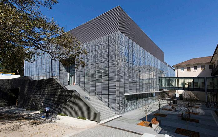
The Sydney Nano Grand Challenges aims to use advances in nanotechnology and nanoscience to provide ground-breaking solutions to some of the world’s greatest challenges. These challenges include:
- Developing a low-cost method to capture enough water from the atmosphere to alleviate the effect of drought by providing water for consumption to humans and animals, and for irrigating plants and crops.
- Reducing CO2 emissions in manufacturing processes and converting CO2 into commercial products through nanocatalysis
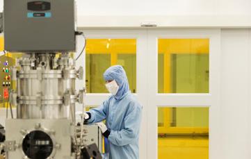
- Developing a regulation framework to assess safety, efficacy and toxicity, and guide future development of nanomaterials, including in drug formulations, food additives and biosensors
- Building autonomous, programmable nanorobots to navigate through the body to detect and treat early signs of disease
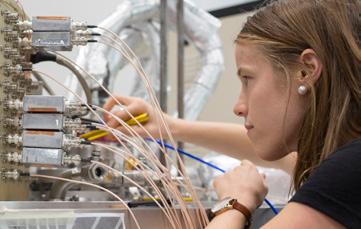
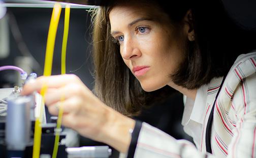
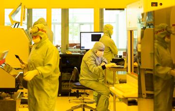
- Simulating new materials from a single atom to fully functioning devices using quantum computers, multiscale simulation, artificial intelligence and machine learning
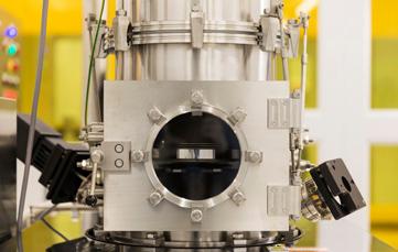
Specifically, research being undertaken by the Nano Institute includes researching the effects of nanoparticles on living organisms. This is critical in order to protect health as well as protect the sustainability and benefits that nanomaterials offer.
Furthermore, research is being conducted in the field of nanoengineered reversible energy storage. Through designing and fabricating nanodomains of electroactive materials, using self-assembly and electrode patterning, and the subsequent interrogation at nanoscale resolution through in situ methods, prototype devices have been developed. As a result, the spin-off company Gelion Technologies was established.
FEATURE –
Nanotechnology
WW W.M ATERIALSAUSTRALI A COM AU BACK TO CONTENTS 51 | JUNE 2020
Sydney Nanoscience Hub. Image credit: University of Sydney.
RMIT’s Micro Nano Research Facility
 Source: Sally Wood
RMIT is home to the Micro Nano Research Facility (MNRF), where extensive nanotechnology research is undertaken. The MNRF, which houses nine laboratories, facilitates the design, modelling, fabrication, packaging and characterisation of micro and nano devices.
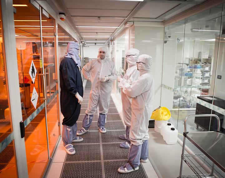
RMIT’s nanotechnology research embraces the interdisciplinary nature of the field and, as such, the MNRF is characterised by its ability to bring together a diverse range of high-quality micro and nano technology into a single facility.
Micro Nanomedical Research Centre
One of the key groups working within the MRNF are the researchers at RMIT’s Micro and Nanomedical Research Centre. Much of the work done at this Centre incorporates miniaturisation, which uses novel physics and engineering to miniaturise laboratoryscale processes and conventional medical procedures and protocols onto chip-scale devices, which can be integrated to form state-of-the-art medical technology.
Their research aims to address some of the most pressing problems regarding current health technology. Furthermore,
RMIT researchers in the micro and nanomedicine field operate within the framework of aiming to improve the availability, accessibility and affordability of point-of-care diagnostics, drug delivery, and biosensors. This could ultimately help to revolutionise the public health sector by providing medical practitioners and healthcare workers with the necessary advanced equipment for the early diagnosis, prognosis and treatment of preventable diseases.
The three key themes of the Micro and Nanomedical Research Centre are: acoustically driven microfluids for biotechnological applications, including diagnostics and biosensing; phononic and photonic nanostructures for enhanced biomolecular detection; and inhaled gene and nanomedicine therapeutics.
The applied research of the Micro and Nanomedical Research Centre has resulted in significant development of completely integrated low-cost portable devices for drug delivery and ultra-sensitive chemical detection, which are some of the smallest available on the market. One of the potential uses for devices such as these for providing new techniques and avenues for roadside testing of illicit drugs.
The team at the Micro and Nanomedical Research Centre are currently performing trials to test and demonstrate the of inhaled delivery of next generation therapeutics such as peptides, monoclonal antibodies, and siRNA, which could prove to be effective for a wide range of pulmonary diseases.
Nano-Earthquakes
In the area of ‘nano-earthquakes’, RMIT University’s Dr Sumeet Walia and Dr Amgad Rezk have examined the use of sound waves to controllably change the electronic properties of 2D materials, in a study led by Dr Sharath Sriram.
The finding has important implications for electronics and optoelectronic devices made from 2D materials, opening the door to a new era of highly efficient solar cells and smart windows.
Other possible fields of applications could include consumer imaging sensors suitable for low-light photography, for example in mobile phone cameras, which currently suffer from poor low-light performance, or in sensors for fluorescence imaging.
Walia, from RMIT’s Functional Materials and Microsystems (FMM) Research Group, said atomically thin semiconductors, popularly called two-dimensional (2D) materials, had been known for decades, but their properties were a relatively new and exciting area for nanotechnology, with many promising applications in nanoelectronics and optoelectronics.
Optoelectronic devices are electronic devices that can interact with, as well as control, light. This property can be harnessed for producing ultrasensitive detectors of light and high-speed phototransistors.
The RMIT research looked at ways of using surface acoustic waves or ‘nanoearthquakes’ to control the properties of 2D materials.
“Sound waves can be likened to ripples created on the surface of water, but where we can control the direction and intensity of these ripples,” Walia, a Research Fellow in the School of Electrical and Computer Engineering, said.
“In this work, we use these ripples which occur on a crystal surface and couple it into
FEATURE – Additive ManufacturingNanotechnology
52 | JUNE 2020 BACK TO CONTENTS WW W.M ATERIALSAUSTRALI A COM AU
a material that is a few atomic layers thick (2D material), which causes a change in its electronic properties.
“As the surface acoustic waves are turned on and off or increased and decreased in intensity, the change in electronic properties of the 2D materials follows the same pattern.”
Rezk, a member of RMIT’s Micro and Nano Physics Research Laboratory (MNRL) and a Research Fellow in the School of Civil, Environmental and Chemical Engineering, said, “A simple technique to control these properties without affecting their inherent chemical and physical characteristics has been a primary scientific hurdle that has hindered their transformation into commercial products.
“We’ve found that ‘nano-earthquake’like waves under the surface of the 2D materials drag electrons along their path, thereby tuning the amount of light emitted by the material.”
“Remarkably, the acoustic wave based tunability did not result in any structural or compositional change in the material.”
“As soon as the acoustic waves were removed, the material retracted back to its initial optical state, and therefore this mechanism is highly adaptable for a variety of dynamically operating systems.”
Metal-Organic Frameworks
Researchers from RMIT have demonstrated a clean, green technique that can produce a customised metal-organic framework, or MOF, in minutes.
MOFs are incredibly versatile and super porous nanomaterials that can be used to store, separate, release or protect almost anything.
Predicted to be the defining material of the 21st century, MOFs are ideal for sensing and trapping substances at minute concentrations, to purify water or air, and can also hold large amounts of energy, for making better batteries and energy storage devices.
Scientists have designed more than 88,000 precisely customised MOFs
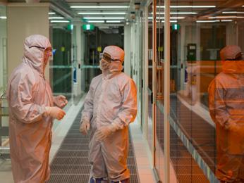
¬– with applications ranging from agriculture to pharmaceuticals – but the traditional process for creating them is environmentally unsustainable and can take several hours or even days.
Dr Heba Ahmed, a postdoctoral researcher in RMIT’s Micro and Nanophysics Research Laboratory, said the efficient and scalable
method harnessed the precision power of high-frequency sound waves.
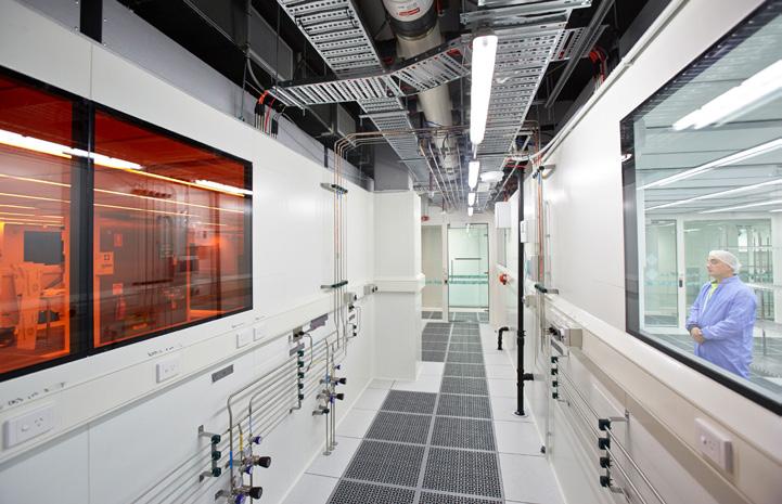
“MOFs have boundless potential, but we need cleaner and faster synthesis techniques to take full advantage of all their possible benefits,” Ahmed said. “Our acoustically-driven approach avoids the environmental harms of traditional methods and produces ready-to-use MOFs quickly and sustainably.”
“The technique not only eliminates one of the most time-consuming steps in making MOFs, it leaves no trace and can be easily scaled up for efficient mass production.”
Metal-organic frameworks are crystalline powders full of tiny, molecular-sized holes. They have a unique structure – metals joined to each other by organic linkers –and are so porous that if you took a gram of a MOF and spread out its internal surface area, you would cover an area larger than a football pitch.
During the standard production process, solvents and other contaminants become trapped in the MOF’s holes. To flush them out, scientists use a combination of vacuum and high temperatures or harmful chemical solvents in a process called “activation”.
In their novel technique, RMIT researchers used a microchip to produce high-frequency sound waves.
The ‘ingredients’ of a MOF – a metal precursor and a binding organic molecule –were exposed to sound waves produced by the microchip.
Using the sound waves to arrange and link these elements together, the researchers were able to create a highly ordered and porous network, while simultaneously ‘activating’ the MOF by pushing out the solvents from the holes.
Lead investigator, Distinguished Professor Leslie Yeo, said the new method produces MOFs with empty holes and a high surface area, eliminating the need for postsynthesis ‘activation’.
The researchers successfully tested the approach on copper and iron-based MOFs, with the technique able to be expanded to other MOFs and scaled out for efficient green production of these smart materials.
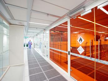
FEATURE – Nanotechnology
WW W.M ATERIALSAUSTRALI A COM AU BACK TO CONTENTS 53 | JUNE 2020
RMIT University’s Micro Nano Research Facility. Image credit: RMIT University.
Melbourne Centre for Nanofabrication Feature
Source: Sally Wood
The Melbourne Centre for Nanofabrication (MCN) combines cutting-edge technology with the skills and experience of expert process engineers to form a world-class nanofabrication centre. MCN is a joint venture that functions in collaboration with six Victorian Universities (Monash University, Deakin University, The University of Melbourne, RMIT, La Trobe University, Swinburne University and Victoria University) and the CSIRO. MCN represents a $50+ million investment in micronanotechnology infrastructure.
MCN is proud to be part of the Australian National Fabrication Facility (ANFF), and is the largest and broadest capability within the ANFF network. Being a node of the ANFF enables MCN to connect with other national research facilities in micro and nanofabrication, allowing for the identification of partners, collaboration and innovation.
MCN provides a pipeline for the design, fabrication, characterisation and testing of nanotechnology materials and devices at a single facility, which enhances productivity and quality gains for users. As such, MCN enables smooth transition from concept to prototype, while also offering the possibility to scale up to trial batch production, which creates a comprehensive user experience.
By providing cutting-edge facilities and end-to-end services, MCN aims to be a world leader for the development and realisation of breakthrough technologies that harness nano and microfabrication.
MCN Services
MCN is home to class 10,000 and class 100 clean room spaces, state-of-theart instrumentation, reconfigurable biochemistry and PC2 laboratories, and a world-class microscopy laboratory.
These facilities enable MCN to provide services in key areas, including:
Lithography
MCN offers a wide range of lithographic techniques and instruments, including:
- Focused ion beam lithography
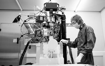
- Electron beam lithography
- Hot embossing
- Nano imprint lithography
- Thermal scanning probe lithography
- PDMS soft lithography
- Direct write lithography
- Photolithography
- Spin coating and wafer development
Thin Film Deposition
MCN offers a wide array of techniques and instruments for thin film deposition, including:
- Atomic layer deposition
- E-Beam evaporation
- Thermal evaporation
- Diamond deposition
- Chemical vapour deposition
- Polymer electronics glovebox
- Sputtering
- Electroplating
- Furnace systems for oxide and nitride growth
Characterisation
MCN features a broad range of instruments for the characterisation and imaging phase of fabrication processes, including:
- Atomic force microscopy
- Scanning electron microscopy
- Spectroscopic ellipsometry
- Laser doppler vibrometry
- Profilometry
- Laser scanning confocal microscopy
- Laser TIRF
- Microspectrometry
- Hyperspectral imaging
Packaging
MCN provides the necessary equipment required for wafer bonding, dicing and wire bonding, which is necessary for the completion of most nano and microfabrication devices.
Etching
MCN houses two Reactive Ion Etching (RIE) systems, which are used extensively in the fields of LEDs, semiconductors, electronics, MEMs, communication technology, microfluids, optoelectronics, and photovoltaics.
Case Studies
A vast array of research is currently being undertaken at MCN in multiple fields. Some of these projects include:
Colour Coded Chemicals
Researchers at La Trobe University, in collaboration with RMIT, have been investigating novel ways to analyse chemicals using visible light. This research has been facilitated by MCN’s facilities. The device they have developed uses the interactions between photons and electrons to filter out colours to create an ‘optical barcode’ that is unique to a sample and can be compared to a library of known material signatures.
The tuneable and potentially portable device can help to quickly identify concentrations of chemicals and can be used for a variety of sensing applications, such as monitoring water pollutants and inspecting soil quality. The device does not chemically change or modify the solution being analysed, which means that it has the potential to be used for real-time monitoring, allowing for applications in food and pharmaceutical production industries.
The device uses microfluidic channels to direct a liquid sample over a silver coating. Light is able to pass through the device thanks to an array of nanometresized holes that feature on the coating. Broadband light is passed through the liquid and is observed from the other side, enabling the identification of a sample. As it passes through the liquid and the array, all but one colour is filtered out, depending on the refractive index of the sample.
FEATURE
– Additive ManufacturingNanotechnology
54 | JUNE 2020 BACK TO CONTENTS WW W.M ATERIALSAUSTRALI A COM AU
Superconducting Diamond
With the help of MCN’s facilities, a Victorian team of researchers has, for the first time in Australia, created superconducting diamond.
Diamonds are an exceptional natural material. They are the hardest naturally occurring substance, they don’t corrode, and they are an incredible thermal conductor. By adding superconductivity to diamond’s list of characteristics offers exciting prospects for a novel class of highly robust devices.
Additionally, superconducting diamond represents a step towards a material that exhibits absolutely no electrical resistance at room temperature, which would be a ground-breaking development in the realm of materials science. Professor Marvin Cohen, an award-winning theorist from the University of California at Berkeley, believes that diamond could be the material to make this achievement possible.
yield enhancement, they show an enormous amount of promise in a range of optical and sensing applications. The main thing currently limiting their widespread uptake is their expensive and laborious production process.
Dr Julian Lloyd, lead author of the research, and his colleagues’ method employs induced electrostatic forces to self-assemble the gold nanoparticle triplets.
This method enables these trimers to be produced with a more than 60% yield – which are unprecedented quantities. Moreover, it removes the need for expensive ‘top-down’ fabrication techniques that have traditionally been used, and which limit the fabrication process’s scalability.
In their research, the team placed differing surface charges on the nanoparticles, which enabled the structures to dram themselves into place.
Back-Contacted Solar Cells
Solar cells are an incredibly promising technology that can help to reduce Australia’s carbon footprint. However, current technologies’ inefficiencies prevent widespread use.
Speeding Up Solar Cell Development
Tests on new designs for perovskite solar cells can now be conducted in minutes instead of days, thanks to a new system built by PhD candidate Adam Surmiak from the ARC Centre of Excellence in Exciton Science (Exciton Science) and his colleagues based at Monash University.
The invention means that the performance and commercial potential of new compounds can be rapidly evaluated, significantly speeding up the development process. The machine, known as a ‘16-channel parallel characterisation system’, can analyse sample perovskite-based solar cells in just 10 to 15 minutes.
Essential to the system’s operation is a series of 3D-printed components that were fabricated with micrometre precision at the Melbourne Centre for Nanofabrication, part of the Australian National Fabrication Facility’s Victorian Node.
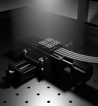
However, producing superconductivity in a diamond at any diamond has proved to be incredibly difficult, with only a few labs around the world achieving it.
A team from the University of Melbourne have joined the elite few who have been successful in doing so. Their research showed that, by adding a dose of boron – a process known as doping – diamond shows superconducting properties at temperatures around 2K.
Using MCN’s diamond chemical vapour deposition capabilities, the team were able to introduce boron which diamond is being grown.
Nanolenses
MCN has played a critical role in providing a team of researchers with the facilities required to enable their creation of a scalable production method for a class of nanoscale lenses using the electrostatic forces between charged nanoparticles, enabling wider application of the technology.
Using the gaps between triplets – or trimers – of different sized nanoparticles, these nanolenses are able to focus light.
Thanks to their miniscule size and very high-
However, a team of researchers working out of MCN have combined the benefits of back-contacted silicone cells and perovskite materials, which offers the possibility for the development of more efficient photovoltaic devices.
The researchers were able to combine the benefits of both back-contacted silicone cells and perovskite-based devices by using a series of photolithography and vacuum deposition processes.
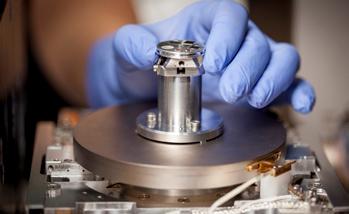
Until now, the combining of a back-contacted design to the perovskite solar cell has proven incredibly difficult because the interdigitated array of electrodes must be delicately structured, which provides a number of major challenges for fabrication.
This novel process, however, enables an alternative design in which the interlocking array of anodes and cathodes are no longer on the same plane, but remain only on one side of the perovskite absorber layer.
As a result, the research has, for the first time, demonstrated the possibility of constructing a back-contacted PSC. While the design is less efficient than what can currently be achieved in conventional siliconbased designs, once optimised these new cells have the potential to provide far higher conversion rates.
Alongside the development and set-up of this new testing facility, Surmiak and the team were also able to significantly speed up the actual solar cell fabrication process.
The head of the Monash University lab in which Surmiak works, Professor Udo Bach, a chief investigator with Exciton Science, described the invention as world-leading. “Our new set-up has the capacity to test thousands of solar cells in one single day, putting us ahead of practically all other R&D labs worldwide,” Professor Bach said.
WW W.M ATERIALSAUSTRALI A COM AU BACK TO CONTENTS 55 | JUNE 2020
FEATURE – Nanotechnology
A detail from the new 16-channel parallel characterisation system. Credit: Adam Surmiak, Xiongfeng Lin.
Short
Courses - Study at Home
Register Now
These short courses provide you with an engaging learning experience. Courses may include flash animations, video of instructors teaching the course in a classroom, video segments from ASM’s DVD series relevant to the learning material, and PDFs of instructor Power Points used in the instructor led training. All online courses require internet access for reading and viewing course content. Both HTML pages and PDF files for each lesson are downloadable and printable for easy offline access. www.materialsaustralia.com.au/training/online-training
BASICS OF HEAT TREATING
Steel is the most common and the most important structural material. In order to properly select and apply this basic engineering material, it is necessary to have a fundamental understanding of the structure of steel and how it can be modified to suit its application. The course is designed as a basic introduction to the fundamentals of steel heat treatment and metallurgical processing. Read More
HOW TO ORGANIZE AND RUN A FAILURE INVESTIGATION
Have you ever been handed a failure investigation and were not quite sure of all the steps required to complete the investigation? Or perhaps you had to review a failure investigation and wondered if all the aspects had been properly covered? Or perhaps you read a failure investigation and wondered what to do next? Here is a chance to learn the steps to organize a failure investigation Read More
MEDICAL DEVICE DESIGN VALIDATION AND FAILURE ANALYSIS
This course provides students with a fundamental understanding of the design process necessary to make robust medical devices. Fracture, fatigue, stress analysis, and corrosion design validation approaches are examined, and real-world medical device design validations are reviewed. Further, since failures often provide us with important information about any design, mechanical and materials failure analysis techniques are covered. Several medical device failure analysis case studies are provided Read More
METALLURGY OF STEEL FOR THE NON-METALLURGIST
This course provides essential knowledge to those who do not have a technical background in metallurgical engineering, but have a need to understand more about the technical aspects of steel manufacturing, properties and applications.
Read More
PRINCIPLES OF FAILURE ANALYSIS
Profit from failure analysis techniques, Understand general failure analysis procedures, Learn fundamental sources of failures. This course is designed to bridge the gap between theory and practice of failure analysis.
Read More
HEAT TREATING FURNACES AND EQUIPMENT
This course is designed as an extension of the Introduction to Heat Treatment course. It discusses advanced concepts in thermal and thermo-chemical surface treatments, such as case hardening, as well as the principles of thermal engineering (furnace design) Read More
NEW - INTRODUCTION TO COMPOSITES
Composites are a specialty material, used at increasing levels throughout our engineered environment, from high-performance aircraft and ground vehicles, to relatively low-tech applications in our daily lives. This course, designed for technical and non-technical professionals alike, provides an overarching introduction to composite materials. The course content is organized in a manner that guides the student from design to raw materials to manufacturing, assembly, quality assurance, testing, use, and life-cycle support Read More
METALLURGY FOR THE NON-METALLURGIST™
An ideal first course for anyone who needs a working understanding of metals and their applications. It has been designed for those with no previous training in metallurgy, such as technical, laboratory, and sales personnel; engineers from other disciplines; management and administrative staff; and non-technical support staff, such as purchasing and receiving agents who order and inspect incoming material.
Read More
PRACTICAL INDUCTION HEAT TREATING
Taking a fundamentals approach, this course is presented as an introduction to the world of induction heat treating. The course will cover the role of induction heating in producing reliable products, as well as the considerable savings in energy, labor, space, and time. You will gain in-depth knowledge on topics such as selecting equipment, designs of multiple systems, current application, and sources and solutions of induction heat treating problems Read More
TITANIUM AND ITS ALLOYS
Titanium occupies an important position in the family of metals because of its light weight and corrosion resistance. Its unique combination of physical, chemical and mechanical properties, make titanium alloys attractive for aerospace and industrial applications. Read More
FEATURE – Additive Manufacturing MATERIALS
AUSTRALIA – Short Courses
56 | JUNE 2020 BACK TO CONTENTS WW W.M ATERIALSAUSTRALI A COM AU
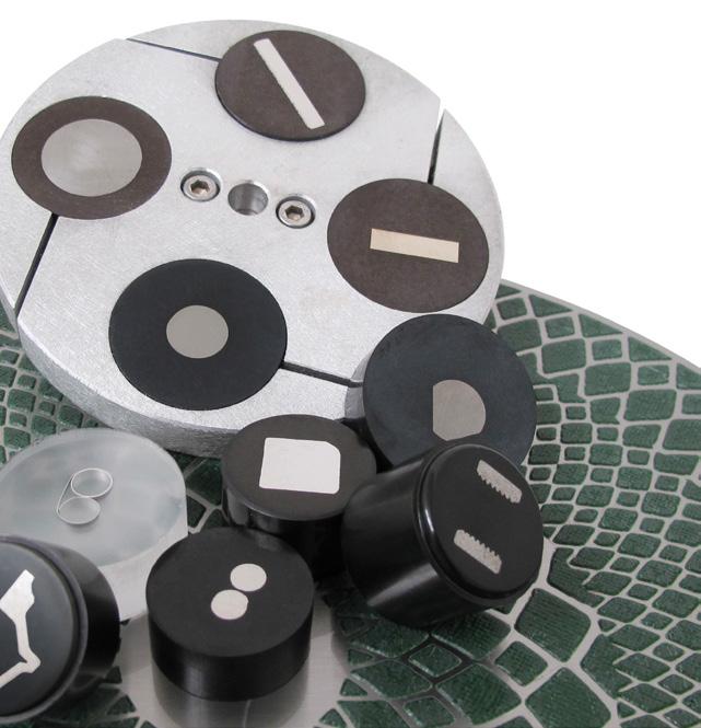
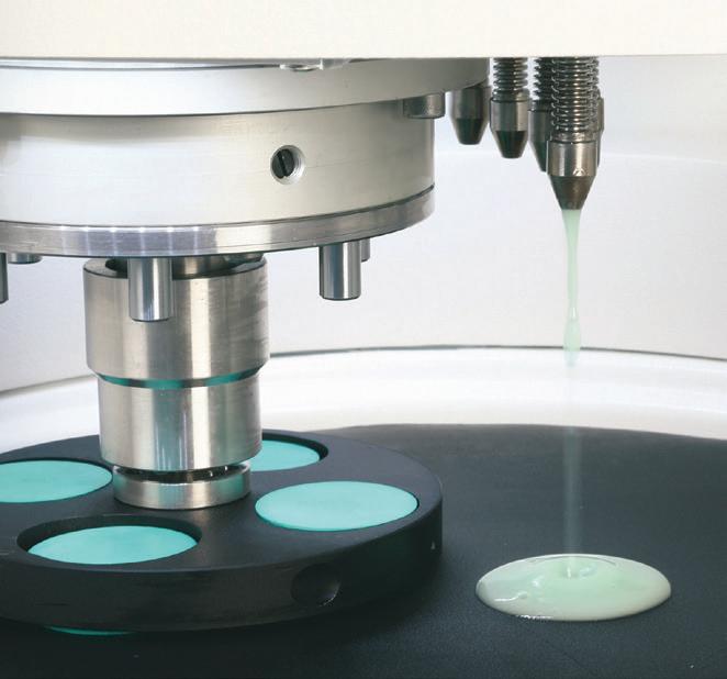

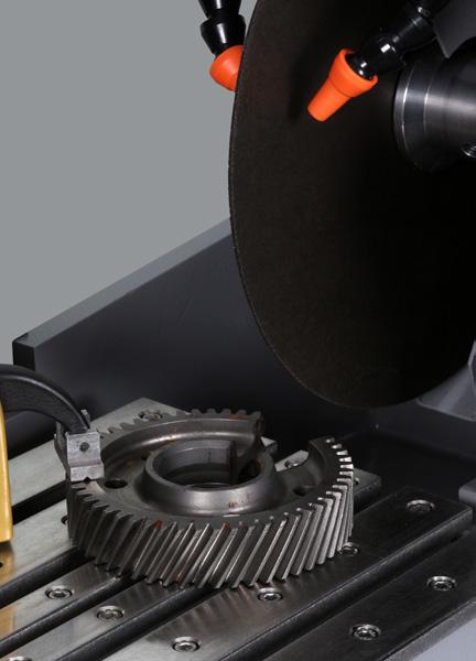
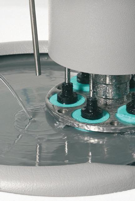
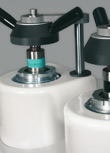
Kemet Australia Pty Ltd, 4/11 Turbo Road, Kings Park, Marayong 2148 (02) 9831 4922 Mob: 0408 222 405 info@kemet.com.au www.kemet.com.au Kemet offer the complete programme of Cutting, Mounting, Grinding and Polishing consumables, Metallographic machines and Ultrasonic cleaning for Metallographic, Metallurgical, Spectroscopic and Geological sample preparation. Easypol is a new diamond suspension and lubricant combination, resulting in faster and simpler metallographic sample preparation. Contact us for a free quotation. Kemet Diamond Products For all your Metallographic Requirements www.kemet.com.au Kemet Precision Lapping | Polishing | Cleaning | Materialography