AI BY DESIGN

SEMI STATE
An expert’s perspective on the current state of the chip industry p.12
TECH ROLES
AI makes transformative impact on Canada’s tech talent p.16
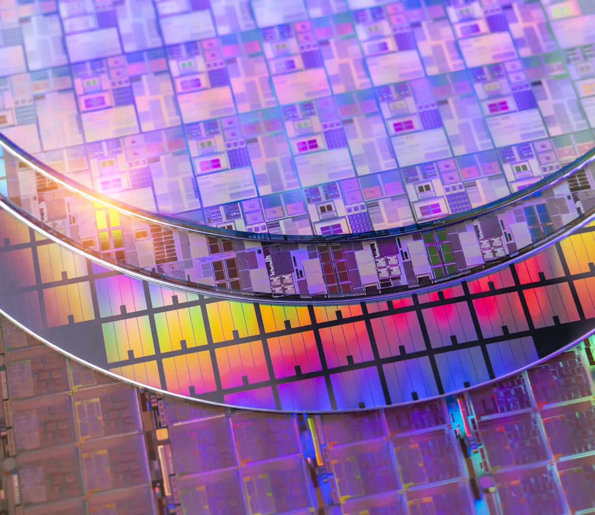
APRIL 2024 CANADA’S INFORMATION LEADER FOR ELECTRONIC ENGINEERS AND DESIGNERS EPT.CA AI TO THE CORE Untether AI combines compute & memory in the semiconductor architecture p.8
intelligence in
engineering
Exploring artificial
the
process p.10


@EPTmagazine April 2024 / EP&T 3 COVER STORY CHIP PERFORMANCE EFFICIENCY Toronto-based semiconductor maker Untether AI sets out to accelerate architecture development AI ASSIST IN DESIGN Industry veteran shares thoughts on using AI in the electronic engineering process SEMICONDUCTORS & AI INTERSECT
Chik details key challenges, opportunities to be aware of with chips and AI AI’S IMPACT ON TECH POOL
intelligence is having a transformative impact on Canada’s tech talent envrionment Columns 4 EDITORIAL AI’s incursion into engineering field 6 WEST TECH REPORT Sonus Microsystems set to transform ultrasound tech 7 THINK GREEN Are all enviro claims equally good? In every issue 5 NEWSWATCH 18 NEW PRODUCTS 20 SUPPLY SIDE 21 AD INDEX 22 DEV BOARDS Raspberry Pi 5 APRIL 2024 8 10 INSIDE Cover photo: Untether AI Photos (this page, from top): Untether AI; gorodenkoff /Getty; ipuwadol/Getty; gorodenkoff/Getty 12 16 8 10 12 16 1812TRX Series Compact Ethernet Isolation Transformers • Comply with 10/100/1000BASE-T, Single Pair Ethernet (SPE), and Power over Ethernet standards per IEEE 802.3 • New chip-style construction in a compact SMT package • Fully automated production for lower cost and increased reliability Request Free Samples @ coilcraft.com EPT_Coilcraft_April24.indd 1 2024-03-13 12:05 PM
Raymond
Artificial
Navigating the evolution: AI’s impact on engineering

As the tech field roars ahead, the relationship between artificial intelligence (AI) and electronic engineering continues to evolve. From conceptualization to implementation, AI is quickly permeating most facets of the design process. This means a fundamental alteration to the way we design, manufacture and utilize electronic systems. This integration heralds a new era of innovation, but it also presents unprecedented challenges and ethical considerations that demand our careful navigation.
and control, pushing the boundaries of what’s possible. By fusing sensor data with AI models, these systems can adapt to dynamic environments, mitigate risks and operate with unparalleled efficiency and precision.This convergence of AI and engineering is reshaping industries, unlocking new possibilities for automation, efficiency, and safety.
Moreover, AI is revolutionizing the field of signal processing, offering innovative solutions for data analysis, compression and communication. With AI-driven algorithms, engineers can extract meaningful insights from vast datasets, enabling advancements in fields like telecommunications,
Despite challenges, the synergy between AI and the engineering community offers boundless opportunities for innovation
At the heart of AI’s impact lies its ability to augment the capabilities of engineering. Traditionally, electronic design required meticulous planning, extensive prototyping, and iterative refinement. However, with AI-powered tools, such as machine learning algorithms and neural networks, engineers can expedite the design process, optimize performance, and anticipate potential flaws with super accuracy. This acceleration not only reduces time-to-market but also empowers designers to tackle increasingly complex challenges, from semiconductor manufacturing to circuit optimization.
Pushing boundaries
One of the most transformative applications of AI is in the realm of autonomous systems. Whether it’s self-driving cars, drones, or industrial robots, AI algorithms are driving advancements in perception, decision-making,
medical imaging, and remote sensing. By leveraging AI’s pattern recognition capabilities, designers can enhance the efficiency and reliability of communication systems, paving the way for faster data transmission, reduced latency, and improved spectrum utilization.
Real world consequences
However, amidst the optimism surrounding AI’s potential, it’s crucial to address the inherent challenges and ethical considerations that accompany its integration into electronic engineering. One of the foremost concerns is the ethical use of AI in certain applicatinos, particularly in autonomous designs where decisions made by AI algorithms can have real-world consequences. Ensuring transparency, accountability and fairness in AI-driven systems is paramount to prevent unintended harm and maintain
public trust.
Furthermore, the proliferation of AI raises concerns about its potential impact on the job market and workforce dynamics. While AI promises to streamline processes and enhance productivity, it also poses a threat of automation, potentially displacing traditional roles and necessitating upskilling and reskilling efforts among engineers. Addressing these challenges requires a collaborative effort from industry stakeholders, policymakers, and educational institutions to foster a workforce that can thrive in an AI-augmented electronic engineering landscape.
Ethical considerations
Despite these challenges, the synergy between AI and the engineering community offers boundless opportunities for innovation and societal advancement. By embracing AI as a catalyst for progress, designers can harness its transformative power to tackle pressing global challenges, from climate change to healthcare, with ingenuity and resilience. Moreover, by prioritizing ethical considerations and human-centric design principles, we can ensure that AI serves as a force for good, empowering us to create a future where technology enriches lives and expands human potential.
Ultimately, the impact of AI is multifaceted and is reshaping the way we conceive, create and utilize our skillsets. By navigating this evolving landscape with foresight, responsibility and collaboration, we can harness the full potential of AI to propel electronic engineering into a new era of discovery and prosperity.
STEPHEN LAW Editor slaw@ept.ca
Canada’s information leader for electronic engineers and designers
APRIL 2024
Volume 46, Number 3
READER SERVICE
Print and digital subscription inquiries or changes, please contact
Angelita Potal
Tel: (416) 510-5113 Fax: (416) 510-6875
Email: apotal@annexbusinessmedia.com
Mail: 111 Gordon Baker Rd., Suite 400
Toronto, ON M2H 3R1
EDITOR Stephen Law slaw@ept.ca · (416) 510-5208
WEST COAST CORRESPONDENT Mike Straus · mike@brandgesture.ca
SENIOR PUBLISHER Scott Atkinson satkinson@ept.ca · (416) 510-5207
ACCOUNT MANAGER Joanna Malivoire jmalivoire@ept.ca · direct 866-868-7089
SALES MANAGER Chander Verma cverma@annexbusinessmedia.com cell 437-218-0941
ACCOUNT COORDINATOR
Shannon Drumm sdrumm@annexbusinessmedia.com
MEDIA DESIGNER Brooke Shaw bshaw@annexbusinessmedia.com
AUDIENCE DEVELOPMENT MANAGER
Anita Madden amadden@annexbusinessmedia.com (416) 510-5183
GROUP PUBLISHER Paul Grossinger pgrossinger@annexbusinessmedia.com
CEO Scott Jamieson sjamieson@annesbusinessmedia.com
EP&T is published eight times per year by
ANNEX BUSINESS MEDIA 111 Gordon Baker Road, Suite 400 Toronto, ON M2H 3R1
Tel (416) 442-5600
Fax (416) 510-5134
annexbusinessmedia.com
SUBSCRIPTION RATES
Canada – $59.67 one year; $95.88 two years
USA – $136.68 (CAD) per year
International – $187.17 (CAD) per year
Single copy – Canada $15.00
ISSN 0708-4366 (print)
ISSN 1923-3701 (digital)
PUB. MAIL AGREEMENT NO. 40065710
Return undeliverable Canadian addresses to:
EP&T Circulation Department, 111 Gordon Baker Rd. Suite 400, Toronto, ON M2H 3R1

© 2024 EP&T. All rights reserved. Opinions expressed in this magazine are not necessarily those of the editor or the publisher. No liability is assumed for errors or omissions or validity of the claims in items reported. All advertising is subject to the publisher’s approval. Such approval does not imply any endorsement of the products or services advertised. Publisher reserves the right to refuse advertising that does not meet the standards of the publication. Occasionally, EP&T will mail information on behalf of industry-related groups whose products and services we believe may be of interest to you. If you prefer not to receive this information, please contact our circulation department.
PRINTED IN CANADA
4 ELECTRONIC PRODUCTS & TECHNOLOGY / April 2024 EPT.CA EDITORIAL
Connect with EP&T magazine @EPTmagazine facebook.com/EPTmag/ /ept-magazine info@ept.ca ept.ca
MIL/AERO
AREA X.O SELECTED AS NATO DEFENCE INNOVATION ACCELERATOR
Area X.O, the R&D complex operated by Invest Ottawa, has been selected as one of 13 NATO Defence Innovation Accelerator for the North Atlantic (DIANA) test centres in Canada. Area X.O accelerates the safe development, testing and adoption of next-gen smart mobility, autonomy and connectivity technologies.
Clients and partners of Area X.O stand to benefit by helping NATO-endorsed innovators and firms test, validate and commercialize promising next-gen technologies, and safely get to market faster. The selection process aims to address global defence challenges and markets by leveraging Area X.O’s unique capabilities and expertise as a certified Public Research Institution under Canada’s Industrial Technology Benefits (ITB) Policy.
NATO DIANA is a global network that facilitates cooperation between military operators and the Alliance’s best and brightest start-ups, scientific researchers, and technology companies. NATO leaders also announced the expansion of this network in Canada, selecting three additional Ottawa-based test centres alongside Area X.O. These include three labs of the National Research Council Canada (NRC), including the Canadian Photonics Fabrication Centre; the Ocean, Coastal and River Engineering facility; and the Digital Technologies Research Centre.
CLOUD & EDGE
KEYSIGHT, AMD BREAK BARRIERS TO REDEFINE BENCHMARKING
Keysight Technologies Inc. leveraged 4th generation AMD EPYC CPUs from Advanced Micro Devices, Inc. to develop an industry first benchmarking methodology that redefines the landscape of system performance evaluation for high-speed digital designers, network equipment manufacturers and data center operators.
The deployment of mobile and 5G private networks require a versatile compute architecture that can simultaneously support millions of

Area X.O helps accelerate the development, testing, validation, demonstration of new security and defence technologydriven products and services.
low-latency, high-bandwidth devices, and a multifaceted workload profile. Given this transformation, comprehensive infrastructure benchmarking is critical to ensure optimal performance across a spectrum of industry use cases, according to Raghu Nambiar, corporate vice-president, data center ecosystems and solutions, AMD.
ELECTRIC VEHICLES
APPLE KILLS EV PLANS
Apple has terminated its plans to develop an electric vehicle (EV) and dissolved the team dedicated to the project. Rumors surrounding Apple’s venture into the electric vehicle market, aimed at challenging competitors like Tesla (TSLA), have circulated for some time, albeit with intermittent references from senior executives.
The decision to abandon the EV initiative, which reportedly employed a substantial workforce, is attributed to its misalignment with Apple’s primary focus on consumer electronics and online services.
SPACE
MDA REBRANDS TO MDA SPACE
Canadian space technology MDA Ltd., has rebranded to MDA Space, an identity evolution that honours the past, recognizes the present and further positions the company to lead in a new era of space innovation.
“The addition of Space to our brand is a natural evolution. The core of our brand identity is, and always will be, MDA – the three iconic letters that stand for our 55-year heritage, our more than 450 missions, and our record of firsts,” said Mike Greenley, CEO of MDA Space.
The global space economy is accelerating and scaling at a rapid rate, growing to $509-billion in 2023 and projected to become a $1.5T industry by 2040.
POWER
APEC SHOW DRAWS DIVERSE ATTENDANCE
Apple has elected to abandon its EV initiative, saying it misaligns with the firm’s main focus on consumer electronics.
The exact financial investment Apple poured into the EV project remains undisclosed.
Speculation regarding Apple’s foray into electric vehicles emerged in 2014 following the recruitment of automotive experts and talent from various car manufacturers worldwide.

The IEEE Applied Power Electronics Conference and Exposition (APEC) concluded its annual gathering last month, marking another successful event for professionals and researchers in the field of power electronics. The event drew a diverse array of attendees, including academics, industry experts and students, all converging to explore the latest advancements, exchange ideas, and foster collaboration in the realm of power electronics.
The four-day event featured a comprehensive program comprising technical sessions, keynote presentations, tutorials, and an expansive exhibition floor showcasing cutting-edge technologies and products from leading companies and research institutions.
@EPTmagazine April 2024 / EP&T 5
NEWSWATCH
Photos: Area X.O; Apple
Sonus Microsystems set to transform ultrasound remote monitoring, diagnostic imaging
Vancouver-based medtech firm, Sonus Microsystems, has unveiled what it is calling the “next generation” of ultrasound technology, delivering remote diagnostic imaging, without the need to go to a clinic or hospital.
The stagnant development of ultrasound transducers, still primarily rooted in piezoelectric technology, poses challenges in the medical sector where sonographers’ expertise is pivotal.
This stagnation underscores the urgent demand for versatile, high-performance and cost-effective solutions to fully unlock the potential of ultrasound technology. Ultrasound devices and services, a nearly $100 billion market growing at a 12% CAGR (BCC Research 2022), find a significant portion in medical therapeutic, surgical, and diagnostic equipment, comprising one-third of the market. Emerging applications represent the highest-growth segment.
Sonus Microsystems is developing and commercializing a novel and proprietary ultrasound technology that utilizes polymer MEMS sensors to send and receive ultrasonic waves. Their transducers are empowered by the innovative polyCMUT technology (stands for polymer-based Capacitive Micromachined Ultrasound Transducers).
This advanced method of manufacturing ultrasonic transducer arrays involves crafting thousands of vibrating micro-drums on different types of substrate, resulting in superior performance for imaging and testing applications.The polyCMUT technology is a leap forward in the ultrasound field, offering enhanced imaging capabilities and a new standard for diagnostic and material testing.
Polymer-based ultrasound transducers
“We are uniquely positioned with over 100 years of ultrasound domain expertise to deliver our cutting-edge customizable ultrasound transducers which enable automated imaging for remote monitoring and wearable ultrasound applications powered by AI diagnosis,” says Dr. Hani Eskandari, CEO and president at Sonus
Microsystems.
monitoring into a reality.
The team, led by four Ph.D.s with extensive experience in ultrasound, nanotechnology and semiconductors – recently announced that they have raised a $2.1M pre-seed round led by LDV Capital. Other investors including several notable angel investors, early-stage funds and ultrasound and AI domain experts have joined the round.
The new funding will be used to enhance processes related to R&D and production, identify new application areas and partnerships, and build a robust engineering team, encompassing fabrication, electronics and software.
From left are:
Carlos D.
Edmond
The company specializes in manufacturing ultrasound transducers tailored for three distinct use cases: disposable and miniature transducers ideal for applications demanding high-quality imaging in limited spaces; flexible and cost-efficient wearable transducers that unlock various healthcare monitoring and screening applications; and large matrix array transducers, offering operator-independent ultrasound imaging for remote monitoring and screening across diverse use cases.
Sonus’s novel matrix technology is paving the way for accessible AI-powered patches that automate ultrasound scanning and measurement and unlock affordable monitoring and screening of patients.
“Our transducers have demonstrated superb performance for medical diagnostic applications requiring a high degree of design flexibility. We are empowering industry leaders and visionary ventures to expedite their NPI timelines, enhance metrics, and explore new markets,” says Dr. Carlos D. Gerardo, co-founder and director of R&D. “By utilizing polymers, we can manufacture polyCMUTs with fewer fabrication steps and minimal equipment, leading to substantial cost savings, swift iteration cycles, and unique capabilities,” he explains.
Charting new frontiers
Sonus Microsystems has recently secured several partnerships in the medical space to develop the tools needed to turn remote diagnostic imaging and
“This advanced imaging and sensing platform is poised to redefine the ultrasound landscape and unlock new remote monitoring applications in healthcare,” says Evan Nisselson, general partner at LDV Capital. “We thrive on investing in people building cutting edge proactive healthcare solutions to hopefully improve people’s lives and deliver significant value.”
Who is on the Sonus team
The core team at Sonus Microsystems includes Dr. Hani Eskandari: Experienced deep-tech entrepreneur with a Ph.D. in medical robotics and ultrasound. Holds over 10 patents; Dr. Carlos D. Gerardo: Expert in ultrasound transducer design, fabrication, and signal processing. Holds 3 patents and received an Excellence in Nanofabrication award in 2018; Dr. Robert Rohling: Current director of ICICS at UBC, founder and CSO of SonicIncytes. Holds over 20 patents and authored 300+ scientific papers;
Dr. Edmond Cretu: Professor in Electrical and Computer Engineering at UBC, with expertise in MEMS devices, circuit design, signal processing, and control. Holds seven patents and authored 150+ scientific papers.
Sonus Microsystems is at the forefront of transforming ultrasound technology with its polymer CMUTs, developing transducers for advanced healthcare, NDT and wearables.
www.sonusmicrosystems.com
6 ELECTRONIC PRODUCTS & TECHNOLOGY / April 2024 EPT.CA
WEST TECH REPORT
Photo: Sonus Microsystems
The leadership team at Sonus Microsystems admires some its next-gen ultrasound technology.
Hani Eskandari, Ph.D. CEO & president
Gerardo, Ph.D. Director of R&D, Co-founder
Cretu, Ph.D. Co-founder
Are all environmental product claims equally valid?
BY MICHAEL S. RICHARDSON, SUSTAINABILITY MANAGER, SGS
Product sustainability is important. It’s not only better for society and the planet, but products with proven sustainability attributes give consumers the power to align purchases with environmental concerns. It also gives businesses much-needed pricing power. How can your business promote product sustainability in a trusted way?
Generational difference
Sustainability is now a key driver in consumer electronic products. A 2021 study found that 61% of core millennials (aged 27-32) wanted to buy from environmentally conscious companies, 58% checked labeling for evidence of sustainability in the form of certification, and 60% intentionally bought items with environmentally preferable or less packaging. This represents a notable shift from baby boomers (born 1946 – 1964), where only 47% looked to buy from environmentally aware businesses, 51% considered eco-packaging as important and 43% looked for evidence of sustainability certification.
Millennials and Gen Z are also willing to pay more for sustainable goods. This is not surprising as they typically espouse social consciousness and environmental justice. A 2023 study found that 80% of consumers would pay more for products at a farmers’ market, bespoke items or products manufactured with a lower carbon footprint. Of the responders, 40% said they were willing to pay up to 10% more, with 10% saying they would pay up to 30% more.
When looking for products, consumers said they were looking for evidence of biodegradability, a reputation for ethical practices, environmentally preferable materials, local production, lower carbon footprint and traceability/transparency.

Greenwashing and other unsubstantiated claims
Naturally, with sustainability a key decision driver for many consumers, products of all types now carry environmental claims. An EU study found that 75% of products now carry an environmental claim or label. However, it is one thing to make a claim to gain sales but another to actually live up to the claim, and research by the European Commission found 42% of green claims were potentially false or deceptive.
This is greenwashing and it can come in many forms, with environmental claims being either lies, unsubstantiated, vague (‘natural,’ ‘sustainable,’ etc.) or irrelevant. It is also possible that factual statements are misleading or legitimate certifications might be applied falsely to products. This all creates distrust and confusion for consumers.
Many governments are starting to respond. For example, the US Federal Trade Commission (FTC) has threatened almost 700 marketing companies with civil penalties if the claims they
make about products cannot be corroborated. Though this warning focused on other claim types, it shows the FTC is watching and willing to act.
The FTC is also revising its ‘Green Guides’. First issued in 1992, these provide guidance to marketers on a range of different product environmental claims. They have been revised multiple times, most recently in 2012, and the current revision may be issued in 2024, which could result in new activity on the issue of greenwashing.
At a time when consumers are actively looking for products that can demonstrate sustainability, there is a real risk that greenwashing will destroy trust, thereby reducing the incentive to make and purchase more sustainable goods, which will ultimately be harmful to the planet.
Solving the problem
Trust is paramount in any transaction. Consumers need to be confident that when they see a claim, they can trust it has been properly substantiated.
To achieve this, claims must be:
• Independently verified/ certified by a third party against internationally recognized standards (ISO 14021, EN13432, EN16640, ASTM D6400, etc.)
• Relevant to the product
• Traceable to allow access to relevant information that confirms claims
Which marks are most relevant?
Environmental claim certification and verification schemes reinforce trust in consumer products by relying primarily on independent testing against recognized standards to assess and demonstrate specific environmental attributes.
Manufacturers and suppliers can choose which marks are most relevant to their product, in consultation with experts. Products are then independently tested and/or audited in accordance with recognized standards and a technical review is conducted by an industry specialist to confirm or refute compliance.
Products that meet the requirements of a relevant claim can then carry an internationally recognized ‘green’ designation. This can be applied to a wide range of products.
For consumers, the single attribute claim makes it easier for them to understand and allows them to align their purchases more easily with ethical requirements.
For businesses, it simplifies the process, making it more focused while helping prevent greenwashing, building trust, enhancing brand image, differentiating products in competitive markets and lowering costs through a onestop solution.
SGS is a global testing, inspection and certification company, recognized as a global benchmark for sustainability, quality and integrity. www.sgs.com/en/ services/sgs-green-marks
@EPTmagazine April 2024 / EP&T 7
THINK GREEN
Photo: simpson33/Getty
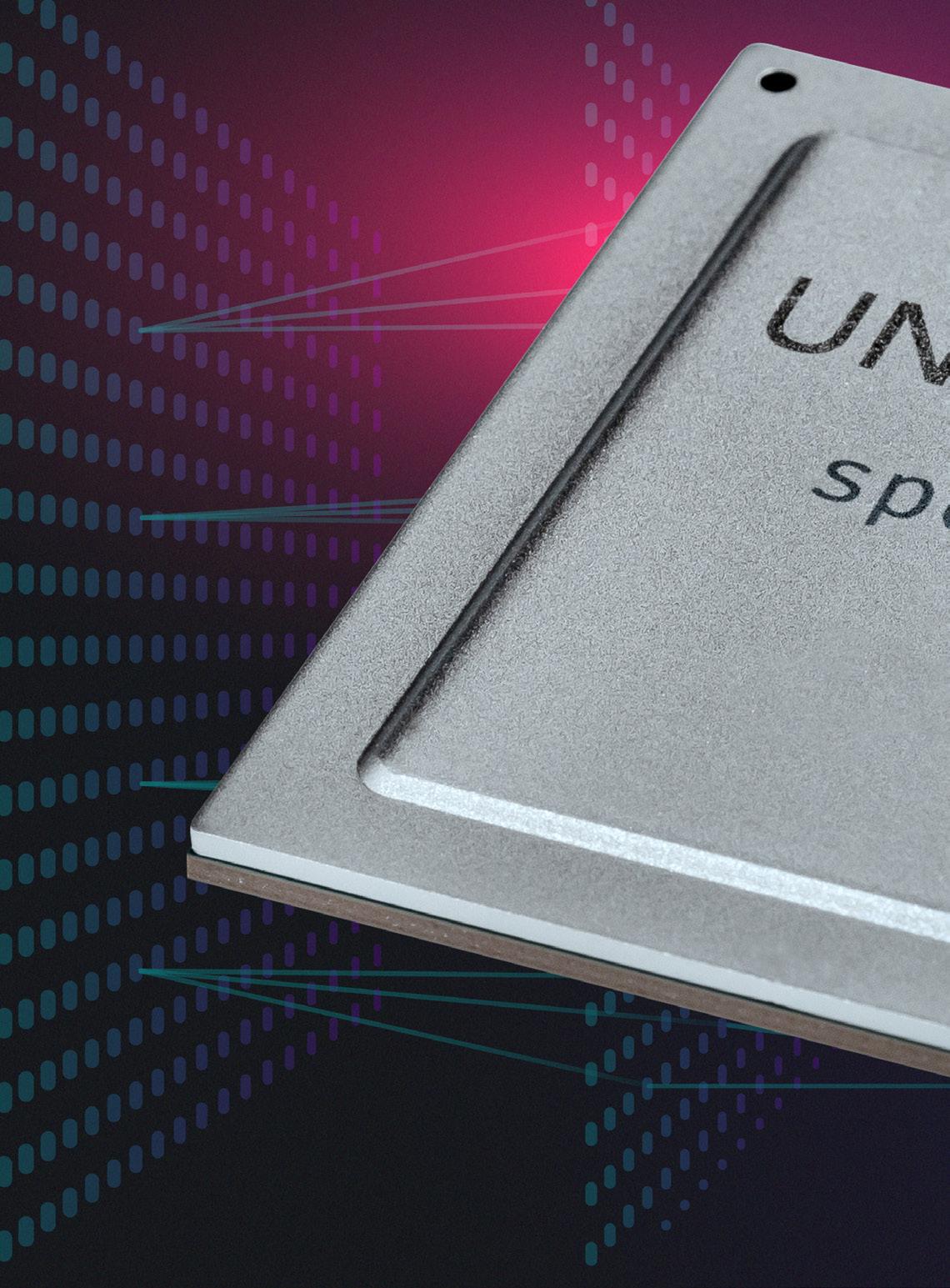
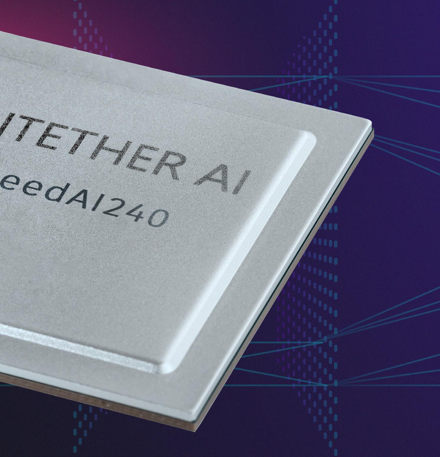
Untethering the development of processors with AI
Toronto chip maker Untether AI accelerates semiconductor architecture advancements
BY STEPHEN LAW, EDITOR EP&T
As the tech industry witnesses an unprecedented explosion of machine learning and generative artificial intelligence (AI) use cases, Canada continues to produce homegrown talent capable of rising with the tide of emerging expertise.
Among these leading players is Untether AI, a Toronto-based semiconductor firm that specializes in developing high-performance AI processors for various applications, particularly focused on deep learning and neural network tasks.
These processors deliver exceptional performance while minimizing power consumption, making them suitable for deployment in edge computing devices, data centers and other AI-driven systems. Untether AI’s technology often involves innovative approaches to parallel processing and memory management, enabling efficient execution of complex AI algorithms. Overall, the start-up firm aims to push the boundaries of AI hardware acceleration, facilitating faster and more energy-efficient computation for a wide range of applications.
“Our firm was founded on the notion that as AI goes into deployment – as it becomes real in the world from training towards inference - we’re focused on inference and making it run – making it work at scale,” said Chris Walker, CEO, Untether AI.
Walker says that in the early adoption days of AI, chips have been running on the multi decades old von Neumann architecture.
“What we do is called At-memory
compute, as we have an array of more than 1,400 processors together with memory and a spatial array on the chip. What differs is, we put the memory and the compute together - where it matters the most for speed and accuracy. In contrast to traditional GPU based architectures, this dramatically reduces the amount of work and energy consumption involved with moving data from external memory, through what are a couple of bottlenecks in traditional architectures into the computation. This is where the real action happens.”
Memory & compute combined
Walker says by putting the memory and the compute together, while building in efficiency – ultimately delivers as much as an 80 to 90% reduction in wasted energy by pushing data through bottlenecks.
“So much energy is wasted just shuffling data around. If we’re going to be using AI in our everyday lives at scale deployment, it has to be energy efficient, it has to be fast, and it has to be accurate,” explained Walker.
At present, the firm processes AI compute workloads at least 15 times more efficiently than the state-ofthe-art chips offered by leading GPU manufacturers. From autonomous vehicles to enabling new enterprise class generative capabilities, demand for AI is an immense opportunity. This is where Untether AI’s ultra-efficient at-memory chip architecture is well-positioned to be a market leader, according to Walker.
The firm’s depth of engineering expertise is fortified by a blend of
talent on the team - both on the hardware and software side. Untether AI draws its strength from staff that have worked with AI start-ups to large scale technology architectures, from FPGAs to microprocessors. Walker has spent most of his career at Intel Corp., and has access to machine learning experts, as well as senior advisors involved in four generations of the tensor processing unit (TPU).

“Most importantly, we have a very rich base of both experience and new students from the University of Toronto and University of Waterloo. That’s a combination that brings together new ideas and experience,” Walker said.
Special time for AI
Founded in 2018, Untether AI has grown from its nascent years of employing 30 people to more than tripling its staff size today.
“I think it is a really special time for AI, as the world’s moving beyond just the training and getting AI developed - to actually making it happen. For us, we think our role is serving as an accelerating ingredient, to be that partner of choice - to enable other streams and applications,” Walker continued. “We think this technology is going to be impactful for the world in terms of energy consumption and usage. As a start-up, we see the spirit of innovation, the spirit of choice,
8 ELECTRONIC PRODUCTS & TECHNOLOGY / April 2024 EPT.CA
ARTIFICIAL INTELLIGENCE FEATURE
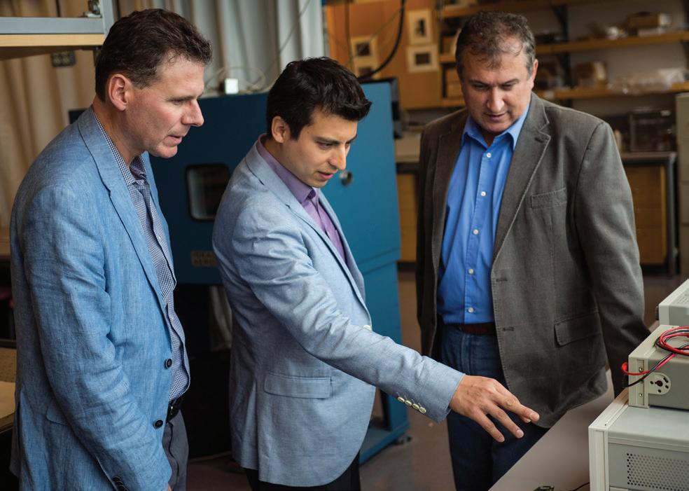
Untether AI’s CEO Chris Walker says his firm combines chip memory and compute, which accerates speed and accuracy.
Photo: Untether AI
in disruption, where things have been dominated by one big player (NVIDIA). It’s a very big market, so there’s a lot of room for more. We think we’ve got a great role to help our customers differentiate from a standardized solution - where there’s only been one vendor. Being a part of our customer’s success is really how I see us playing in the future, and what I think our role is.”
OEMs and on-premise data centres have begun using the firm’s AI inference ICs and AI accelerator cards to deploy artificial intelligence just about anywhere, noted Walker.
“I think from a design and implementation perspective, the semiconductor industry is often creating devices for use-cases and capabilities that the end-market doesn’t quite know they need yet. So, you have to be ahead of the curve of envisioning what the capabilities need to be, and what are going to be the important factors,” Walker said. “In our case, we believe it’s computing power, that’s energy effective, because if you want to do things at scale, you can’t be infinitely building out data centres and adding power plants, while cooling them as well.”
As a relatively small and nimble company, Walker says Untether AI operates within a very transparent internal culture – functioning as open and collaborative with customer issue
Untether AI is a member of the UCIe chiplet standard consortium that defines the interconnect between chiplets within a package.
an infrastructure that permits us to run it on today’s chips, or a simulation of the future chips. With that, we can start development with them in real time,” Walker stated. “So, we can run a test model, to gauge performance and determine what they might iterate. That’s the interesting part, as you start with your own ideas of the product. It’s really when you engage with customers, that you see the impact it has. And, it makes us better in terms of what customer support is necessary, such as network development, tools and flows. It’s an iterative and collaborative process to make it all happen.”
Moving forward in the next two years,Walker says his team will rapidly grow off the baseline it has established and continue to support markets anywhere from enterprise data centre to automotive and a chiplet approach.

resolution.
“In some customer-use cases, they might be a few years out before they deploy our technology. But, they’re looking at architecture today. They understand what it can do in the future. A big part of what we strive to achieve, is to be a great partner for our customers, to listen - to adapt. There’s fantastic new technologies and enablers coming out, like chiplets and standard interconnects, that are going to enable us to do that, and still retain our focus on being the most efficient and effective,” added Walker. With customers in Canada, Europe and across North America, Untether AI partners in different ways. One is just on the delivery of its product, while others involve more in-depth engagement including collaboration on designing the test infrastructure, which is typical in the hardware ecosystem. The firm also teams-up with clients around the world on industrial, automotive, aerospace applications, which primarily focuses on software.
Run a test model
“We need to find what they want to do in their neural networks. We have
Untether AI is a member of the newly formed consortium behind the UCIe chiplet standard (Universal Chiplet Interconnect Express), an open specification that defines the interconnect between chiplets within a package. This enables an open ecosystem and ubiquitous interconnect at the package level. Other prominent board members include Alibaba, AMD, Arm, Advanced Semiconductor Engineering.
“Today, most products like ours are developed at the silicon level - which then gets put in a package – and then put on a board,” Walker said. “Chiplets are designed in a ‘Lego style’, which allows a customer to create their system with multiple different components in one package.”
As the (UCIe) standards are being established, and Untether AI remains at the forefront of those standards, Walker is confident that this will help his team stay on the cutting edge when working with others and how they want to imagine their products.
“This enables customers to achieve what they want, and not have to do the whole solution themselves. Together, including AI, brings the ‘bestof-the-best’ in terms of inference acceleration, which really opens the door for new applications and new deployments,” concludes Walker. www.untether.ai/
@EPTmagazine April 2024 / EP&T 9
Exploring the impact of AI in electronic design
BY BRIAN SATHIANATHAN, CO-FOUNDER & CHIEF TECHNOLOGY/DIGITAL OFFICER, ITERATE.AI
AI’s capability to automate intricate tasks, sift through extensive datasets for insights, and foster innovation in design is revolutionizing the way engineers and designers will approach their work. From refining the architecture of printed circuit boards to advancing predictive maintenance in manufacturing, AI’s role is extensive and impactful. As we examine the potential of AI, it becomes evident that it is set to redefine the electronics industry, offering unprecedented opportunities for growth and innovation.
One of the most significant benefits of AI in electronic design is its ability to automate repetitive tasks. Using machine learning algorithms, AI can quickly analyze vast amounts of data, identify patterns, and make predictions, freeing up engineers and designers to focus on more creative and high-level work. For instance, AI can aid in the design of printed circuit boards (pcbs), automating the routing process and optimizing component placement for maximum efficiency.
AI is also being used to improve the manufacturing process. By analyzing data from sensors and machines, AI can identify potential issues before they become problems, reducing downtime and increasing productivity. For example, AI-powered predictive maintenance can detect anomalies in machine performance, allowing engineers to address issues before they cause equipment failures or production delays.
AI also continues to make a significant impact in the design of electronic devices, as AI-powered tools assist with the creation of more sophisticated and innovative products. AI-generated pcb designs
can reduce production costs and improve performance. AI can also help optimize power consumption, thermal management, and other critical factors in the design process.
But AI’s impact on the industry goes beyond just design and manufacturing. AI-powered tools are also being used to enhance the user experience. For example, AI-powered voice assistants like Amazon’s Alexa and Google Assistant have become increasingly popular, allowing users to control their devices with voice commands. AI is also being used to improve the visual interface of devices, such as AI-powered display adjustments that can automatically adjust brightness and color based on ambient lighting conditions.
The potential benefits of AI in the field of electronics and design are staggering. According to a report by ResearchAndMarkets.com, the global AI in electronics market is expected to grow at a CAGR of 22.4% from 2020 to 2027, reaching a total market size of $10.4 billion by 2027.
The adoption of AI in the industry also raises some challenges. One of the biggest concerns is the potential loss of jobs for human engineers. However, while AI may automate some tasks, it’s unlikely to replace the need for human expertise entirely. Instead, AI is likely to augment human capabilities, enabling engineers and designers to focus on more complex and creative work.
Another challenge is the need for high-quality training data. AI algorithms require vast amounts of data to learn and make accurate predictions, and the quality of this data is crucial. The industry must invest in collecting and labeling high-quality data to ensure that AI-powered tools

can make accurate predictions and decisions.
Industry impact

“AI-driven design tools have introduced a level of optimization in product development that was once beyond reach.” - Iterate. ai co-founder
Brian Sathianathan
As the industry continues to evolve, it’s crucial to invest in high-quality training data and address concerns about job displacement. The symbiotic relationship between AI and human expertise will shape a more innovative and efficient landscape, and the future of electronics and design will look brighter than ever.
AI’s ability to process and analyze data at scale allows for the exploration of design configurations previously deemed unattainable. Notably, AI’s role in generative design illustrates this point vividly. By optimizing for multiple objectives, AI-driven tools can yield design solutions that balance conflicting requirements, such as minimizing weight while maximizing structural integrity.
Research published in the Journal of Machine Learning in Engineering highlights cases where AI-generated designs outperformed traditional solutions by 10-15% in efficiency metrics, underscoring the potential for innovative breakthroughs.
10 ELECTRONIC PRODUCTS & TECHNOLOGY / April 2024 EPT.CA
ARTIFICIAL INTELLIGENCE FEATURE
Photos: gorodenkoff/Getty; Iterate ai
In the domain of materials science, AI’s predictive capabilities are ushering in a new era of electronic component development. AI algorithms, through their analysis of vast datasets, can forecast the properties of novel materials, potentially revolutionizing the industry with materials that provide improved performance and sustainability. A recent study in Advanced Materials Technologies showcases how AI identified a new composite material that improved battery life in electronics by 20%, a testament to AI’s transformative potential in material innovation.
Showcasing AI efficiencies
Quality assurance and product testing also benefit markedly from AI integration. Traditional testing methodologies often fall short in their coverage of potential failure modes, whereas AI, by learning from historical data, can predict future failures with heightened accuracy.
This predictive approach not only enhances product reliability but also significantly reduces time to market. Data from a report by the International Journal of Electronic Quality
Management indicates that AI-driven testing strategies can reduce testing cycles by up to 30%, showcasing AI’s efficiency in ensuring product quality.
Discourse surrounding AI in electronics also necessitates a discussion on ethical considerations and the imperative for responsible AI usage. The adoption of AI solutions must be guided by principles of transparency, fairness, and accountability to prevent biases and ensure trustworthiness in AI-powered decisions.
The IEEE’s guidelines on Ethically Aligned Design offer a framework for addressing these concerns, emphasizing the importance of ethical standards in the development and deployment of AI technologies.
The shift towards AI-enhanced electronic design demands a recalibration of skills and knowledge within the workforce. As AI technologies evolve, so too must the competencies of engineers. The necessity for continuous education and skill development in this area is critical.
A report by the World Economic Forum predicts that 85% of jobs in 2030 have not yet been invented, highlighting the urgent need for
adaptive learning and training programs focused on AI and its applications in electronics.
The integration of AI into electronic design and manufacturing presents a multifaceted opportunity for innovation, efficiency, and quality enhancement. Supported by empirical data, these points underscore the profound impact AI is poised to have on the industry, as a whole. As we navigate this technological evolution, addressing ethical considerations and investing in workforce development will be pivotal in realizing the full potential of AI in shaping the future of electronics and design.
Where do we go from here?
The changes brought about by AI span across automation, data analysis, design innovation, and even the fundamental approach to problem-solving within the sector. Engineers are now equipped with tools that not only enhance efficiency, but also open new avenues for creativity and innovation.
Integration of AI into electronic design presents a multifaceted opportunity for innovation.
Automation can relieve engineers from the tedium of repetitive tasks and advanced data analysis capabilities have led to more informed decision-making, drawing on insights that were previously inaccessible due to the sheer volume of data.
AI-driven design tools have introduced a level of optimization in product development that was once beyond reach, resulting in products that are not only more efficient but also more aligned with goals.
The predictive maintenance capabilities of AI have shifted manufacturing processes, reducing downtime and increasing productivity. However, these advancements also come with their set of challenges, including the need for continuous learning and adaptation among professionals to keep pace with rapidly evolving technologies.
BILLION
The global AI in electronics market is expected to grow to $10.4B by 2027.
As the sector continues to navigate these changes, the focus must remain on leveraging AI’s potential responsibly and ethically, ensuring that the benefits of these advancements are realized broadly across society.
Iterate.ai is a Silicon Valley-based software firm that develops artificial intelligencepowered low-code software designed to accelerate innovation projects within large enterprises.www.iterate.ai/
@EPTmagazine April 2024 / EP&T 11
Semiconductors and AI intersect
Raymond Chik details key challenges and opportunities to be aware of
As artificial intelligence (AI) continues to gain a foothold in all technology sectors globally, semiconductor development is in lockstep with the revolution. Innovation in this space is accelerating at breakneck speed, as market demands evolve, while geopolitical factors and supply chain challenges nip at the heels of chip designers today.
In order to gain some insights to this topical issue, EP&T sits down with Raymond Chik, PhD and consultant with DRC Enterprises , providers of business solutions, from financial budgeting and planning, start-up guidance, institutional marketing, as well as governance, risk management and compliance (GRC) consultancy.
Adding to his relevancy in this conversation, Chik is a highly regarded semiconductor design engineer, serial entrepreneur and an angel investor. He completed his PhD in electrical & computer engineering from the University of Toronto in 1995.
Can you provide an overview of the current state of the semiconductor industry and its significance in the rapidly evolving field of technology?
The current state of the semiconductor industry is characterized by the interplay between technological innovation, rapidly evolving market demands, geopolitical factors and supply chain challenges – recent geopolitics has forced the once well-established global semiconductor supply chain into two separate supply chains – China and the West. This is highly inefficient and anti-capitalism in exchange for national securities.
From the market perspective, as we come into 2024, the global semiconductor industry is heading into a recovery from the downturn in 2023. This is partly due to the rebound of the memory chip market. Of course one significant driving force that is fuelling the semiconductor market is artificial intelligence (AI).

How do you perceive the intersection of AI & semis shaping the future?
Semiconductors are the basic building block of the Hardware infrastructure that all AI models/applications train and run/ deployed on
AI and semiconductors are extremely important to each other. In fact, I would say that the main reason for the rapid development of artificial intelligence is because of semiconductors. AI has been around for a long time, but only in recent years, with the advent of semiconductor compute chips, in particular GPUs, the amount of computational performance/ required to train and run AI neural network models became adequate. This also partly triggered the explosion of LLM and generative AI in the past year, because now there are hardware infrastructures powered by these compute chips available for training and running these big models possible.You’d still need tens of thousands of GPU chips to train and run them; but at least it’s feasible.
Can you highlight some key challenges and opportunities in the chip business?
Here are a couple of key challenges that I see:
• Supply chain inefficiency due to geopolitics; the de-globalization and on-shoring or supply chain will have a significant pricing effect on semiconductor products – we will see more expensive electronic products.
• Talent shortage: the need for skilled-workers in the semiconductor industry will be growing and companies often have difficulties filling qualified candidates with relevant experiences to fill their open positions.
Some opportunities that I see:
• Advance packaging technologies: while the industry is pouring tons of investment into keeping the Moore’s Law alive, the advancement silicon chip packaging technology has not been progress at nearly the same rate as silicon wafer processing technology. This has changed over the past few years where advanced packaging technologies are starting to provide a new and better way to improve chip performances. Techniques such as
12 ELECTRONIC PRODUCTS & TECHNOLOGY / April 2024 EPT.CA FEATURE ARTIFICIAL INTELLIGENCE
Photo: ipuwadol/Getty
Fan-Out wafer-level-packaging (FOWLP), 2.5D and 3D die-stacking technologies allow new avenues for chip makers to create high performance products without only resorting the process node advancement through Moore’s Law.
• The rise of AI: this is a no-brainer. It has been predicted that by 2032, the AI HW market will grow from about US$30B from 2022 to >US$600B in 2023. This explosive growth will be a tremendous fuel to semiconductors made for AI.
• Automotive industry growth: this is another huge growth area for semiconductors. The shift towards EV (electric vehicles) and autonomous driving, particularly battery management systems and ADAS, will create an increased demand for semis designed for automobiles.
AI is transformative in various sectors. What role will semis play?
As mentioned, semiconductor chips are the basic building block of the hardware (HW) infrastructure that all AI models/applications are trains and run/deployed on, from the compute servers in the cloud/data-centers to the micro-power chips right at the extreme edge – sensors and such. So semiconductors not only play a pivotal, but an essential role, in advancing AI technologies.
Can you elaborate on the specific areas that deep tech is making an impact?
Here are a few specific domains where significant innovations and advancement driven by semiconductor and AI:
• AI accelerators: this is the obvious one; AI, and therefore semiconductor chips running AI, everywhere is the trend
• Energy efficient semiconductors: power consumption by chips is
an essential metric is paramount regardless of whether they are operating in the extreme edge all the way to data center servers, using energy harvesting, batteries and grid power
• Advanced sensing technologies & Edge AI: In the realm of IoT, and autonomous systems especially for industrial applications, advanced sensing technologies such as LiDAR/radar/ imager/force/position, coupled with edge AI, very low power, AI chips capable of processing data right at the edge where the data is captured.
• Next gen memory:
• Start-ups are working in photonics chips, where light is used instead of electrons to transmit data and signal potentially offering faster and more efficient data processing. Many semiconductor start-ups are exploring integrated photonics for applications in data communications and processing.
What role does angel investing play in fostering innovation in deep tech?
Building a semiconductor startup is a capital intensive venture, especially if you’re in the market where advanced processing nodes are required for computationally intensive markets, such as AI and HPC. I see Angel investors with a relevant industry background/experience, being able to provide some capital, while also sharing previous industry start-up experience.
In Canada, there are not enough Angel investors with deep semiconductor industry knowledge to help foster the deeptech start-up ecosystem. But, I believe that over the past 10-15 years, there are a growing number of successful Canadian semiconductor entrepreneurs who can be contributing to the angel or early stage start-up investment community/ecosystem.
How do you assess the investment landscape for start-ups working on the cutting-edge?
While AI has been the hype and continues to be the darling for VCs to invest into, I’m not sure how sustainable the trend is. As mentioned, semiconductor start-ups are generally capital intensive and certainly the hype around AI has led to investors paying more attention to semiconductor start-ups with some form or shape of AI angle. In particular, the capital market has experienced a major downturn and re-calibration of startup valuations, which have been overly-inflated during the 20202021 boom. This year will see a slight up-tick, with tech stocks performing well generally as well as the anticipation of the return of some IPO activities. However, no one is expecting a return to the ‘glory’ days of 2020-2021. The current state of minds of VCs are one of ‘back to the basics’ , like 5-6 years ago. Dry-powder is still out there, but VC’s are putting more scrutiny in assessing the business cases, strategies and revenue potential of growth stage startups (Series B and beyond). However, AI and semiconductor related start-ups are still one of the hottest area where VCs are willing to invest in.
As an angel investor, what criteria do you consider essential when evaluating potential partners in semiconductors or AI technologies?
First and foremost I look at the founding team. I don’t prefer a solo-led team. It’s very hard for one person to have all the skill-sets required to navigate the complex natures of a AI semiconductor start-up.
The questions I would ask is how well do the founders know each other. What is their track-record - do they have the relevant technical expertise and experience.
The next thing would be the technical innovation. Does their idea solve a significant problem
that is not already managing an existing technology? Is there an obvious market requirement for such as solution? Is there a real market need for it (or is it just a fancy science project)? Obviously, there are many more questions that I would ask, such as business/revenue model, scalability, go-to-market strategy and financial projection, etc. The first three things are the most important ‘screen-test’ to for me.
The semi supply chain has faced challenges recently. How will that impact the deployment of AI, and what strategies can businesses adopt to mitigate?
Deglobalization of the supply chain and on-shoring of manufacturing are the most significant impacts I can see. On the one hand, it will significantly impact the cost structure coming from a sub-optimal use of resources which will likely result in increase of cost of semiconductor manufacturing, which in turn would increase the HW cost for deploying AI solutions. We had been facing chip supply shortage over the past few years, but this is easing. The semiconductor industry is known to be cyclical, and inventory is already building up now. It is also expected that the global semiconductors fab capacity will be drooping back to the 70% level.
With the global focus on sustainability, how are semis and AI aligning with environmental goals?
There has been a realization of the energy required to train and deploy AI models on compute HWs will create an energy consumption concern. It is predicted that up to 20% of the global energy consumption by end of the decade will be dedicated to datacentre compute HW, most AI being most of the workload. Many AI researchers and chip designers are spending a lot of time in creating more energy efficient AI models and hardware. There will be a major driving
@EPTmagazine April 2024 / EP&T 13
Semis & AI cross paths
Cont’d from page 13
force to deploy more energy efficient AI models, as well as semiconductor HW. Therefore, investors should be looking out for start-ups that are focused on creating energy efficient AI solutions.
Can you share any success stories or breakthroughs you’ve encountered in the deep tech sector?
I started my semiconductor design career in the mid-90’s after I finished my PhD. Early in my career, as a chip designer, I had designed one of the first PRML Read Channel chip for Hard Disk Drive applications. Since then, while still doing a lot of hands-on design, I’ve also been building up my semiconductor start-up career as a serial entrepreneur
To date I either founded or was a member of a founding team of five semiconductor start-ups, with two exits. My latest start-up Untether AI (see cover feature), perhaps my favourite one yet, makes industry-leading energy efficient chips & hardware (HW) for AI inference.
The field of quantum computing is gaining attention. How do you envision its integration with semis and its potential impact on AI applications?
The use of semiconductor-based qubits, instead of binary bits of a classical computer, in quantum computers, is a major R&D area. However, to-date most semiconductor based quantum computers are either superconducting qubits or quantum dots, both require cooling down the circuits to absolute 0 or a few Kelvin - which require sophisticated cryogenic cooling systems. This is one of the main challenges in quantum computing - to be able to scale computing and AI applications to mainstream.
However, there are other ways to make qubits, such as through photonics. The photonic qubit based quantum computer has
been gaining traction, as it operates at room temperature and photonic qubits inherently have lower error-rates. This is because photons do not react with each other as strongly as matter-based qubits, leading to easier quantum error correction.
Photonics are also intimately related to semiconductor technologies as in recent years, the integration of photonic systems with silicon technology has been prolific.
Whether it’s superconducting qubits or photonics qubits, quantum computing is expected to have a profound impact in future AI development, as it delivers a new compute infrastructure that enhances the speed and accuracy of AI systems.
What advice would you give to semiconductor start-ups aiming to navigate the competitive market and attract investment?
For a semiconductor deep tech start-up, in fact as with any other start-up, one of the most important thing is to have a strong team of founders. Not only the technical backgrounds have to be relevant and solid, the founding team members, typically two to four, would be best to have complimentary skill sets and experiences. Then you want to be very clear on what problem you’re trying to solve
start-up founders, they must be laser-sharp focused on getting customer traction and interest as much as possible early on.
One vital point that I cannot stress enough is ‘get your first-silicon out the door’ as quickly as your can – forget about making it perfect. The key is to place a product on your potential customers’ hands; get their feedback and apply the learnings back to your next generation product.
Looking ahead, what emerging trends or advancements do you foresee?
and the solution you’re providing is unique and ideally no one else is offering a similar solution to the market (that’s the ‘story’).
Equally important, also, is your IP/patents. For any deep tech start-ups, it’s typically very important to patent protection because that’s your secret sauce and probably your market differentiator(s). Fundraising at early/pre-seed stage means that you’re selling the Team and Solution as a ‘story’ to the right investors who are familiar with the hardware/ semiconductor business – so they’re not scandalized by the ‘pre-revenue’ mode.
The main difficulty for semiconductor & hardware start-ups in raising early stage / pre-seed or seed rounds is the time-to-revenue is usually a very long road , possibly a few years – this scares away many software/SaaS centric investors. Therefore often times a semiconductor/hardware startups would raise it’s early stage funding only on a story or the founding teams track-records/ credentials and through corporate / strategic VCs who are already familiar with your business.
That being said, with the current ‘recalibration’ of the capital market from the 2020-2022 ZIRP booms-day era, VCs are much more cautious about capital deployment. For early stage / pre-seed/ pre-revenue
What I see as emerging trends in the forthcoming years withing the AI and semiconductor sectors are as follows, some if not all of those I had already touched on previously.
• Compute-Chips & HW optimized for AI workload:
• This is what I see as ‘what’s beyond GPUs’.
• Advanced packaging:
• Keeping up with Moore’s law through advancement in semiconductor process technology has become an uber expensive endeavor, advanced 2.5D and 3D packaging offer potentially a much ‘wider’ avenue for improvement chip performance and IO bandwidth especially many of AI compute applications (such as LLM and G en AI) are very much memory BW bound.
• Edge AI:
• As we see more and more AI chips and HW made to be highly energy efficient, integrating AI/ inference acceleration HW on edge devices will be prolific, reducing the heavy loading to cloud-based services. These advancements will likely lead to a future where technological landscape where real-time smart processing becomes more integrated into everyday devices and services.
Raymond Chik, PhD, is a consultant with DRC Enterprises, providers of a wide range of business solutions.
14 ELECTRONIC PRODUCTS & TECHNOLOGY / April 2024 EPT.CA FEATURE ARTIFICIAL INTELLIGENCE
Photo: kynny/iStock / Getty Images Plus
Demand for AI optimized chipsets to spur hybrid bonding
Requirements for technology spreads across the semiconductor industry
The rapid rise of new artificial intelligence (AI) applicationsboosted recently by broad interest in generative AI (GenAI) - is having a dramatic impact on the semiconductor industry. It is accelerating demand for compute capacity that will outpace the capabilities of current chipset technologies underpinning today’s high-performance infrastructures, platforms and devices, according to Dr. Seung Kang, vice president of strategy at Adeia, a leader in the semiconductor intellectual property (IP) arena.
Rising interest in AI across nearly every vertical segment of the global digital economy is expected to drive a surge in demand for hybrid bonding technology across the semiconductor industry.
According to analysts at Gartner, semiconductors designed to execute AI workloads represented a USD$53.4 billion revenue opportunity for the semiconductor industry last year, an increase
of 20.9% from 2022. AI-centric semiconductor revenue will continue to experience double-digit growth over the next few years, increasing 25.6% in 2024 to $67.1 billion and reaching $119.4 billion by 2027.
AI workloads are computationally intensive
“AI is dramatically impacting the industry because it is accelerating the need for increasingly powerful and energy-efficient computing systems, surpassing the capabilities of incumbent semiconductor platforms,” said Kang. “AI workloads are computationally intensive, demanding semiconductor systems that are customized for massive parallel computing.”
Currently, the key drivers of such systems are a graphics processing unit (GPU) and high-bandwidth memory (HBM) which are coherently integrated with high-speed interconnects. To meet state-of-the-art AI system requirements, unprecedented performance benchmarks are

needed. This is especially true when dealing with large language models. However, both processors and memory components face fundamental semiconductor scaling challenges.
“GPUs and AI-customized neural processors rely on cutting-edge logic nodes that offer a smaller footprint, lower power consumption and faster speed. As the demand for computing performance continues to grow, realizing such processors on a monolithic chip -- even at the most advanced node -- becomes increasingly challenging. In such cases, the desired approach is to disaggregate and reassemble chips in new form factors without significant trade-offs,” Kang said.
There is a growing consensus in the industry that hybrid bonding technology will become widely adopted both for processors and for HBMs. Compared with other methods, hybrid bonding offers inherent advantages in high-density IO (input-output), reduced parasitic delay, shorter height and improved thermal performance.
Hybrid bonding is a method to interconnect semiconductor

wafers or dies by combining metal-to-metal and dielectric-to-dielectric bonding. It is commonly associated with Direct Bond Interconnect (DBI?, DBI? Ultra).
Hybrid bonding explained
Hybrid bonding is a direct bonding technology that interconnects wafer-to-wafer, dieto-wafer and die-to-die at an ultra-fine pitch without the need for solder or other adhesives.
“Hybrid bonding finds applications today in 3D heterogeneous integration scenarios where different types of chips –designed for different functions or from different suppliers – are seamlessly integrated and made interoperable. The evolving requirements of AI systems are expected to surpass the capabilities of conventional semiconductor system architectures,” explained Kang. “This trend is driving the industry towards adopting disaggregated multi-chip configurations. Hybrid bonding is well-positioned as a compelling technology to underpin and facilitate these innovative semi conductor architectures.”


@EPTmagazine
FEATURE
ARTIFICIAL INTELLIGENCE dynamicsourcemfg.com Electronics Manufacturing Services Canada: 403 516 1888 | USA: 602 833 8591 Don't Let Uncertainty Define Your Production Eliminate worries with timely deliveries and transparent communication. Master your supply chain with DSM for seamless operations and unmatched efficiency. EPT_Dynamic_April24.indd 1 2024-03-19 11:41 AM
Redefining tech roles
The transformative impact of AI on Canada’s tech talent
BY QAISER HABIB, HEAD OF CANADA ENGINEERING, SNOWFLAKE
From a renaissance of traditional technology roles in the race to enhance GPU efficiency - to reimagining the ‘data scientist’, AI is evolving the roles of tech workers and decision-makers around the globe — and it will largely be for the better.
Here in Canada, we benefit from having very deep technical talent that continues to be in high demand. As roles change across our industry, the need to upskill and be open to the emerging opportunities that AI brings will not only allow Canada’s tech talent to keep pace, but also position itself at the forefront of the current data and AI revolution.
Let’s dig into how specific roles are evolving in the age of AI and what this means for the C-suite, as this paradigm shift not only revolutionizes technical work, but also presents changes for leaders and job roles across all fields.
Demand for hardware designers
While hardware designers were once in high-demand during the microprocessor era in the 1970s and 80s, we have come full circle and it is once again a highly sought after position amid the AI boom — creating efficient accelerators and processors built for AI workloads.
Currently, hardware is the blockade to accelerating AI, and the ultimate moat over the next few years will be GPU costs and innovation. As AI models become more powerful, their usefulness will depend on equally powerful and innovative hardware to break down existing barriers to AI entry. This means jobs like chip designers and microprocessor designers are

making a big comeback as companies race to make GPUs faster and more cost efficient – with hardware design becoming a coveted and highly compensated skillset in the process.
To be able to leverage new opportunities, upskilling is necessary. One key area includes becoming proficient in programming languages, specifically Python, which has become one of the most popular and commonly-used programming languages in the field of AI due to its ease of learning and readability, vast libraries and frameworks, versatility, and its ability to integrate with other technologies and languages.
Another key area for hardware designers looking to upskill is in data analysis and data science. Having a deep understanding of how data influences AI algorithms helps designers make comprehensive data-driven decisions on model training and validation, optimization techniques, and ensuring the data compatibility of system integrations.
The role of the data scientist redefined
A common complaint in data science is that a lot of the work is basic, boring data prep — and it’s been a deterrent to young tech talent entering the field. When we speak to students and job candidates, we often hear this narrative and the reality is that much of this prep work, which is considered uninteresting, will be automated by AI.
The AI revolution will transform the role of the data scientist, empowering them to do more than ever before — and have more fun. Moving beyond models and analysis, they will be equipped to create end-to-end full stack applications without the need of a traditional software engineer. They will also be able to go from creating the dashboard, to prompting the large language model (LLM), to surfacing the answers to questions correctly faster and more efficiently, meaning more room for creativity and deeper analysis.
As old problems fall away,
new challenges emerge such as how to feed the right information into the LLM, how to minimize hallucinations, and how to better integrate privacy and security as AI can now also help with sensitive use cases where models often get free reign to train on large data sets. As this role continues to evolve, upskilling will be required to stay relevant. For example, it will be key for the modern data scientist to understand how to select and integrate the right external vendors of AI models.
Efficiency will be a game changer for developers
The role of the developer is also rapidly evolving and largely centers on the ability to increase efficiency through AI when writing code. As a point of reference, Snowflake’s CIO Sunny Bedi asked his development team to estimate how much of the code they are currently writing could be handled by an AI tool, and the consistent answer was 30%. While this is only an estimation, the actual number is likely much
16 ELECTRONIC PRODUCTS & TECHNOLOGY / April 2024 EPT.CA
ARTIFICIAL INTELLIGENCE FEATURE
Photo: gorodenkoff/Getty
higher if we account for reusability and sharing, as AI-generated code can be leveraged for other projects. Even testing and quality assurance can be assisted by AI tools in the future.
While enhanced efficiency is a real game-changer, we still need coders to code at this stage. And for developers to stay relevant and benefit from advancing AI technologies, developers can upskill in a number of ways such as learning prompt engineering, gaining basic model skills on how to train and run models quickly, and investing in integrations between their existing tools with modern technologies like copilots. Attaining certifications to ensure up-to-date learning is also a key factor.
BI analysts will go deep
Business Intelligence (BI) analysts will be forced to uplevel as generative AI and LLMs evolve their roles from creating and reviewing reports to deeper analysis and solving the challenges AI can’t. Today’s analysts generally create and present a canned report, following up with new queries when an executive has a specific supplemental question.
With AI, analysts can now go a step further with the insights generated from the data and determine what actions to take on those insights since the data presentation and analysis is already taken care of.This will unburden analysts’ workloads and free up time to work on deeper questions — bringing their own expertise to what the organization should be analyzing.
A more hands-on executive team
Beyond technical roles, AI is also having a significant impact on the C-suite, as leaders will be more hands-on by extracting data-driven insights available at their fingertips thanks to generative AI-driven applications.
With the increasing sophistication of AI tools, business
executives can leverage advanced natural language processing capabilities to interact with data and receive real-time data analysis that helps make better business decisions. This shift will reduce the reliance on traditional business analysts, as C-suite leaders gain the ability to independently access and interpret complex data patterns, enabling quicker decision-making and strategic planning.
Not only will leaders be empowered to develop robust models, but they will also facilitate the seamless integration of these models into user-friendly interfaces, allowing executives to harness the full potential of AI to drive value.
Building our AI-ready workforce
While we are still in the early stages of understanding AI’s implications on our workforce, one aspect is very clear — traditional linear career paths in our respective tech fields are being replaced by dynamic roles, where a willingness to embrace emerging AI technology is essential. This shift not only fosters a deeper synergy between technology and traditional business roles, but also empowers individuals to embrace creativity, enabling them to delve into deep analyses that can solve complex problems.
A strong, AI-ready workforce in Canada relies on our tech talent to stay adaptable, upskill, and recognize the opportunities AI presents. This will support continued innovation within our technology ecosystem, produce insightful business decisions, and keep Canadian tech workers in high demand.
Qaiser Habib currently serves as Head of Canada Engineering at Snowflake. Habib is a veteran engineering leader and a well-recognized expert in the Canadian market, currently focused on building and leading the Canadian engineering presence for Snowflake. www.snowflake.com/en/

USB 3.1 (10 Gb/s)
High-speed data transfer
The new LEMO USB 3.1 connectors were developed to satisfy the most demanding connection requirements for high-speed data transfer using the USB protocol up to 10 Gb/s. They complete LEMO’s extensive portfolio for robust and durable High-speed solutions and testify to the company’s long experience in signal integrity.
• Max data speed transfer 10 Gb/s
• Compliant USB 3.1 protocol
• Push-Pull latching mechanism
• 360° screening for full EMC shielding
• Compact design for space savings
• IP50, IP66, IP68
• Temperature range: -55 to 250°C
• Mating cycles: > 5000
• Alignment Key: 12 different keyways
• Robust and miniature
LEMO Canada Inc.
Phone : 905-889-5678
info-canada@lemo.com
www.lemo.com/contact
facebook.com/lemoconnectors linkedin.com/company/lemo-sa
@EPTmagazine April 2024 / EP&T 17
® ®
1 2024-03-18 2:47 PM
FAST AND FABULOUS New cutting-edge High-speed connectors EPT_Lemo_April24.indd

35MW LOW POWER DISPLAY SERVES MOBILE DEVICES
DISPLAY VISIONS
EA TFT024-23ATNN 2.4-inch TFT colour display is suitable for mobile use due to its low energy consumption. Device requires 10mA power consumption at 3.3V and shows sharp contrasts even in sunlight. It is very easy to read both with and without backlight. Without backlight, the power consumption is 35mW. During an eight-hour working day, this burdens a LiPo battery with less than 75mAh. The positive TFT panel with a white background can be operated both in colour and in black and white.
www.lcd-module.com
BRIDGE FOR DIN RAIL CONNECTORS OPTIMIZE USE OF INSTALLATION SPACE
PHOENIX CONTACT
Bridge for DIN rail connectors optimize use of installation space. The transmission of data and signals for applications without a necessary output to the pcb can be looped through by a bridge for DIN rail connectors below the module. This enables user to maximize the use of the pcb surface. Device features 8-position module communication and is available in the widths 18.8, 20 and 25mm. Product can be integrated into device applications based on ME-IO and ICS housings. Device delivers maximum pcb surface. Connection of the positions in the field with FMC connectors.
www.phoenixcontact.com/ en-us/products/electronics-housings

SOLDER FUME FILTRATION SYSTEM CLEANS AIR IN PRODUCTION AREAS
WELLER TOOLS
ZeroSmog Shield Pro Fume Extraction System prioritizes clean air for workers in the electronics manufacturing industry. Unit captures solder particles and gases, providing clean air at individual workstations. Featuring EPA E10 filters for particulates and activated carbon for gases, this filtration system supports the health and well-being of workers, allowing them to breathe easy while focusing on their soldering tasks.
www.weller-tools.com
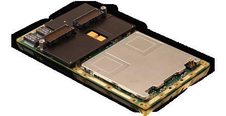
MODULE SPEEDS INTEGRATION OF TRUSTED, SECURE PROCESSING FEATURES CURTISS-WRIGHT
TrustedCOTS plug-in modules brings trusted and secure processing to rugged deployed VPX-based systems with the introduction of the XMC-529 AMD Ultrascale+ MPSoC XMC Mezzanine Card. Module speeds the integration of advanced system IP into VPX, ATX and legacy VMEbus systems. Product can also be used to increase a system’s overall compute power by providing FPGA co-processing to the baseboard. Firm optimizes system architecture flexibility for deployed solutions and provides a common advanced trusted and secure framework that can be deployed using the XMC-529, the previously introduced XMC-528, or via the on-module FPGA devices hosted on its VPX boards.
www.curtisswrightds.com/ products/computing
FOOD GRADE EPOXY DELIVERS ENHANCED CHEMICAL RESISTANCE
MASTER BOND

EP42HT-2FG
Black two part, moderate heat cured epoxy provides high temperature resistance that complies with FDA 21 CFR 175.105 for indirect food contact applications. Product withstands exposure to a wide range of harsh chemicals, including acids, bases and solvents. It possesses enhanced flow properties and can be employed for bonding, sealing, potting and casting. Compound has a relatively long working life of 105-150 minutes for 100 grams of the mixed material at 75°F. Product cures optically opaque and the recommended cure schedule is overnight at room temperature, followed by a heat cure at 150-250°F for 3 to 4 hours.
www.masterbond.com/tds/ ep42ht-2fg-black
SPRING PIN SOCKET DELIVERS 60GHZ ELECTRICAL BANDWIDTH
IRONWOOD ELECTRONICS
60GHz Spring Pin Socket for CSP64 shortest spring pin, 1mm compressed height, provides high electrical bandwidth 60GHz with lowest inductance of 0.17nH along with 2A continuous current carrying capacity. Quarter turn spring loaded lid allows gradual pressure to CSP with easy chip replacement functionality.
www.ironwoodelectronics.com/ press/60ghz-spring-pin-socket-forcsp64
12-BIT OSCILLOSCOPES ADDRESS SIGNAL FIDELITY CHALLENGES SIGLENT
Models SDS800X HD and SDS1000X HD and SDS3000X HD series oscilloscopes improve signal fidelity, visualization and analysis, each equipped with advanced 12-bit
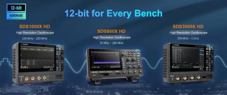
analog-to-digital converters (ADCs) and provide signal quality. With bandwidths ranging from 70MHz to 4GHz, units deliver improved signal fidelity for a wide range of applications including power, EMI, frequency analysis, embedded design and failure analysis. Units deliver a combination of low noise, gain accuracy and channel isolation. Products are typically specified at just 70µVrms noise at 200MHz bandwidth. The lower ranges are specified at 1.5% dc gain accuracy with the ranges ≥5 mV/div having a leading 0.5% accuracy.
www.siglentna.com
ROTARY ENCODER DEBOUNCE IC ELIMINATES NOISY OUTPUTS
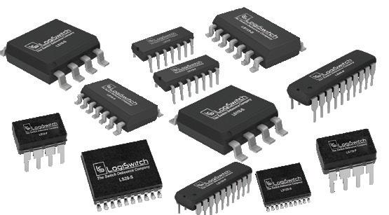
LOGISWITCH
LS30 IC removes noisy switch bounce induced signals from incremental rotary encoders, while including new functionality to indicate the direction of rotation. The small 8-pin IC (available in LTH and SMT packages) eliminates the board space taken up by conventional solutions while adding innovative new capabilities. The rotary encoder-specific IC incorporates firm’s adaptive NoBounce Technology. Device also includes a classic NoBounce Technology-based debounce channel for use by rotary encoders that include a pushbutton switch.
www.logiswitch.com
SMD FUSE DELIVER OVERCURRENT PROTECTION IN STANDARD SMD SIZES BOURNS
SinglFuse Model SF-0603SP-R and Model SF-1206S-RSeries SMD fuse line play a pivotal role in power-based applications. Model
18 ELECTRONIC PRODUCTS & TECHNOLOGY / April 2024 EPT.CA DESIGN SOURCE
NEW PRODUCTS

SF-0603SP-R compact overcurrent protectors are suitable for applications that operate at 48Vdc, and the Model SF-1206S-R Series is suitable for 12Vdc or 24Vdc operating systems where the operating current is over 10A. Devices provide effective overcurrent protection in standard SMD sizes ranging from 0402 to 3812. Product series feature various voltage and current ratings, a wide operating temperature range and high-performance fuse characteristics.
www.bourns.com/products/circuit-protection/singlfuse-smd-fuses
AUTOMOTIVE-QUALIFIED 400V/600V RECTIFIERS DELIVER POLARITY PROTECTION
TAIWAN SEMICONDUCTOR
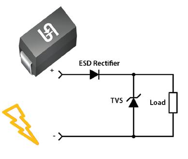
TSD Series automotive-qualified 400V / 600V rectifiers features ESD withstand capability. Devices simultaneously provide repetitive peak reverse voltage (VRRM) of up to 600V as well as ESD protection of >10,000V (per IEC-61000-4-2). Devices provide optional current ratings of 1A, 2A, and 3A and operating temperature ranges from -40°C to ±175°C. All have a maximum forward voltage drop of 1.1V and feature low-reverse leakage current and fast response time.
www.taiwansemi.com/en/automotive-qualified-400v-600v-esd-capability-rectifiers/
MPU DELIVERS AI INFERENCE OF UP TO 80 TOPS WITHOUT COOLING FAN
RENESAS ELECTRONICS
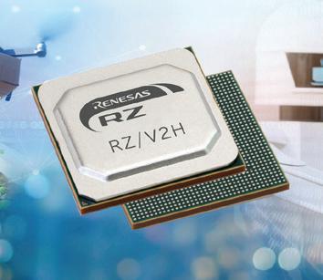
RZ/V2H microprocessors (MPUs) target high-performance robotics applications, delivering high levels of performance and enables both vision AI and real-time control capabilities. Device comes with DRP (Dynamically Reconfigurable Processor)-AI3, delivering 10 TOPS/W power efficiency, a 10-fold improvement over previous models. Pruning technology is employed in the DRP-AI3 accelerator improving AI computing efficiency, boosting AI inference performance up to 80 TOPS. This boost allows engineers to process vision AI applications directly at edge AI devices without relying on cloud computing platforms.
www.renesas.com/us/en
TINY TIME-OF-FLIGHT SENSORS DELIVER 672X804-PIXEL RESOLUTION
STMICROELECTRONICS
VL53L9 all-in-one, direct Time-of-Flight (dToF) 3D LiDAR (Light Detection And Ranging) module with market-leading 2.3k resolution can accurately measure the distance to objects in a scene, and are driving new capabilities in smart devices and industrial automation. Device delivers a resolution of up to 2.3k zones. Integrating a dual scan flood
illumination, the LiDAR can detect small objects and edges and captures both 2D infrared (IR) images and 3D depth map information. It comes as a ready-to-use low power module with its on-chip dToF processing, requiring no extra external components or calibration.
www.st.com/en/imaging-and-photonics-solutions/vl53l9ca.html?icmp=tt37520_gl_ pron_feb2024
To Be Creative

Strip Series B300
Powerful, Efficient, and Intuitive Stripping Machine
Schleuniger’s portable Strip Series B300 delivers fast and reliable stripping of wires with crosssections from 32 to 8 AWG. The machine‘s ergonomic design and intuitive user interface offer unrivaled ease of use, while repeat accuracy, mechanical precision, and short process cycles ensure maximum productivity.
Compact modular design
High-resolution 5” color touch screen
LED lighting for clear view of work area
Highly sensitive trigger mechanism
High process reliability
Wire Solutions for a Connected World
@EPTmagazine April 2024 / EP&T 19
EPT_Schleuniger_April24.indd 1 2024-03-21 11:06 AM
schleuniger.com 905-827-1166

DISTRIBUTION
MOUSER MARKS 60TH ANNIVERSARY
Mouser Electronics Inc., an authorized global distributor with the latest electronic components and industrial automation products, has marked its 60th year in business.
Mouser began with a couple of employees working out of a garage in El Cajon, California, and today ranks as a top 10 global distributor and multi-billion-dollar corporation with 4,000 employees and 28 locations worldwide.
Much has changed in the electronics industry since 1964, but Mouser has remained dedicated to providing the newest technology to customers as quickly as possible.
Mouser Electronics president and CEO Glenn Smith, who joined the company in 1973, attributes Mouser’s success to the hard work of the Mouser team and its dedication to providing best-in-class service. “I congratulate all Mouser employees, past and present. We would not be here today without the exceptional teamwork of our people. They are the backbone of our longevity. Each of us continues to play an important role in making our company thrive,” said Smith. “Together, we have accomplished great things, and we are far from finished.”
“I always tell employees that ‘satisfied customers’ made their paychecks possible,” Smith added. “Our customers and manufacturer partners are a big part of Mouser’s success story. We are extremely grateful for their patronage and partnership.”
ACQUISITIONS
TELEDYNE TO ACQUIRE ADIMEC
Teledyne Technologies Inc. has entered into an agreement to acquire Adimec Holding B.V. and its subsidiaries. Adimec, founded in 1992 and headquartered in Eindhoven, Netherlands, develops customized high-performance industrial and scientific cameras for applications where image quality is of paramount importance.
“Adimec possesses uniquely complementary technology, products and customers in the shared strategic focus areas of healthcare, global defense, and semiconductor and electronics inspection,” said Teledyne CEO Edwin Roks. “For decades and from our own X-ray imaging business headquartered in Eindhoven, I have watched Adimec grow to become a leader in niche applications requiring truly accurate images for precise decision making in time-critical processes.”
RENESAS ACQUIRES PCB DESIGN SOFTWARE PLAYER ALTIUM
Renesas Electronics Corp.has entered into an agreement to acquire Altium Ltd., leading global provider of electronic design automation (EDA) software.
The deal would enable two industry leaders to join forces and establish an integrated and open electronics system design and lifecycle management platform that allows for collaboration across
component, subsystem and system-level design. The transaction strongly aligns with Renesas’ digitalization strategy and represents the company’s first significant step in bringing enhanced user experience and innovation at the system level for electronics system designers.
CIRCUITRY
TECH GROUPS COLLABORATE ON CRYOGENIC CIRCUITS
Fujitsu has collaborated with QuTech for the development of what it is calling “the world’s first” cryogenic electronic circuits for controlling diamond-based quantum bits. Enabling convenient operation of both the qubits and the control electronics in a compact cryogenic refrigerator, the new technique addresses the ‘wiring bottleneck’ in cooling qubits while maintaining high quality performance, marking a significant milestone toward the realization of larger-scale quantum computers.
QuTech will present the results of the joint research project with Fujitsu at the International Conference on Solid State Device Circuits ISSCC 2024 (IEEE International Solid-State Circuits Conference 2024),” this February.
SEMICONDUCTORS
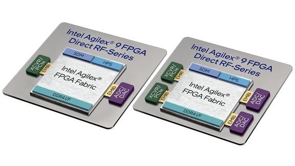
INTEL LAUNCHES STANDALONE FPGA COMPANY
Intel has officially launched Altera, its new standalone FPGA company. Intel executives recently unveiled the firm’s strategy to secure leadership across a $55 billion-plus market opportunity; to expand the company’s portfolio, including the only FPGA with AI built into the fabric; and to help solve mounting customer challenges. The company’s new brand was also announced.
“As customers deal with increasingly complex technological challenges and work to differentiate themselves from their competitors and accelerate time to value, we have an opportunity to reinvigorate the FPGA market,” said Altera CEO Sandra Rivera. “We’re leading with a bold, agile and customer-obsessed approach to deliver programmable solutions and accessible AI across a broad range of applications in the comms, cloud, data center, embedded, industrial, automotive and mil-aero market segments.”
WIRELESS
NEOCORTEC SIGNS DISTY DEAL WITH DIGIKEY
NeoCortec, manufacturer of low-power bi-directional wireless mesh network modules, has signed a global distribution agreement with DigiKey. NeoCortec’s NeoMesh wireless network modules are based on a decentralized mesh of self-governing nodes which are not dependent on a network coordinator. A virtually limitless number of nodes can be added to an existing network. This means that even the largest buildings can be covered with only one network and without any additional infrastructure. NeoMesh utilizes time-synchronization between the nodes, allowing nodes to sleep and wake up efficiently only when required. Most of the time the nodes are asleep with their radio turned off. However, at scheduled intervals the radios wake up to listen for messages and to send messages if required, before going back to sleep again. This approach results in an average power consumption of typically only a few 10s of micro amperes, enabling battery powered operation on a single set of two AA batteries for several years.
20 ELECTRONIC PRODUCTS & TECHNOLOGY / April 2024 EPT.CA SUPPLY SIDE
Photos: Mouser; ;Adimec; Intel; NeoCortec


@EPTmagazine April 2024 / EP&T 21 PRODUCT SOURCE GUIDE TO ADVERTISE in an upcoming issue of EP&T, contact Chander Verma, Sales Manager, cverma@annexbusinessmedia.com | 437-218-0941 Joanna Malivoire, Account Manager, jmalivoire@ept.ca | direct 866-868-7089. AD INDEX ABSOPULSE Electronics Ltd. 21 BEA Lasers . . . . . . . . . . . . . . . . . . . . . . . . . 21 Blockmaster 21 Coilcraft 3 Digi-Key Corporation IFC Diverse Electronics . . . . . . . . . . . . . . . . . . . 21 Dynamic Source Manufacturing 15 EPTech 2024 IBC Hammond Mfg Co. . . . . . . . . . . . . . . . . . OBC LEMO Canada Inc. 17 Master Bond Inc 21 Schleuniger, Inc. . . . . . . . . . . . . . . . . . . . . . 19 Transducers USA 21 EPT_AbsopulsePS_April24.indd 1 EPT_BlockmasterPS_March24.indd 1 2024-03-06 11:38 AM • Toughened system • Electrically isolating • Thermally conductive +1.201.343.8983 • www.masterbond.com Room Temperature Curing TWO COMPONENT EPOXY Supreme 11AOHT EPT_MasterBondPS_April24.indd 1 2024-03-13 12:54 PM Flat Pack Laser Low Profile; Easy Mounting; Alignment Laser Laser Head Rotates and Tilts for Exact Alignment BEA Lasers New Quartz Window E²L Alignment Laser for Extreme Environments! offers a quartz anything you it to! BEA Lasers New Quartz Window E²L Alignment Laser for Extreme Environments! offers a quartz anything you expose it to! (847) 238-1420 www.bealasers.com 1400 Howard Street Elk Grove Village, IL 60007 Phone: 847.238.1420 www.bealasers.com The “FLAT PACK” Laser from BEA Lasers 1.93” (L) x 1.26” (W) x 0.88” (H) Aluminum Housing Red or Green: Dot or Line Pattern Power Supply Included New Product EPT_BEAPS_Aug20.indd 1 2020-07-23 5:42 PM EPT_BEAPS_.indd 1 2023-03-27 1:12 PM @EPTmagazine January/February 2024 / EP&T 25 Flat Pack Laser Low Profile; Easy Mounting; Alignment Laser Laser Head Rotates and Tilts for Exact Alignment Visit our website, request a catalog, or give us a phone call for additional information BEA Lasers New Quartz Window E Alignment Laser for Extreme Environments! (847) 238-1420 www.bealasers.com BEA’s lens offers a quartz glass barrier to anything you BEA Lasers New Quartz Window E Alignment Laser for Extreme Environments! (847) 238-1420 www.bealasers.com BEA’s lens offers a quartz glass barrier to anything you (847) 238-1420 www.bealasers.com Phone: 847.238.1420 www.bealasers The “FLAT PACK” Laser from BEA 1.93” (L) x 1.26” (W) x 0.88” (H) Aluminum Housing Red or Green: Dot or Line Pattern Power Supply Included New Product EPT_BEAPS_Aug20.indd 1 2020-07-23 5:42 PM EPT_BEAPS_.indd 1 2023-03-27 1:12 PM EPT_BlockmasterPS_Nov23.indd 1 2023-10-23 10:56 AM EPT_AbsopulsePS_JanFeb24.indd 1 2023-12-19 1:08 PM EPT_bllockMaster_BEAlaser_JanFeb24_CSA.indd 1 2023-12-14 10:11 AM +1.201.343.8983 ∙ main@masterbond.com www.masterbond.com SILVER FILLED, ONE PART EPOXY EP3HTS-TC offers superior THERMAL CONDUCTIVITY OF 16-17 W/(m•K) • Not premixed & frozen • NASA low outgassing • Very long open time at room temperature EPT_MasterBondPS_JanFeb24.indd 1 2023-12-11 2:33 PM EPT_diverseElec_PS_JanFeb24_CSAPT_bllockMaster_BEAlaser_JanFeb24_CSA.indd 2 2023-12-14 10:17 AM (847) 956-1920 www.TUSAINC.com PANEL MOUNT BEEPERS & BUZZERS In Stock! Competitive Prices! Free Samples! IP65 RoHS High Audio / Lighted Output! Listen to Our Product Selection Online! EPT_JanFeb_Tusainc.indd 1 EPT_TransducersPS_April23.indd 1 Untitled-2 1 2023-12-21 9:14 AM PRODUCT SOURCE GUIDE TO ADVERTISE in an upcoming issue of EP&T, contact Chander Verma, Sales Manager, cverma@annexbusinessmedia.com | 437-218-0941 Joanna Malivoire, Account Manager, jmalivoire@ept.ca | direct 866-868-7089. AD INDEX ABSOPULSE Electronics Ltd. 25 Advanced Interconnections. . . . . . . . . . . . . 5 BEA Lasers . . . . . . . . . . . . . . . . . . . . . . . . 25 Blockmaster . . . . . . . . . . . . . . . . . . . . . . . 25 Coilcraft 23 Digi-Key Corporation IFC Diverse Electronics 3, 25 EPTech 2024 Event IBC Hammond Mfg Co OBC Interpower Corporation . . . . . . . . . . 18 & 19 LEMO Canada Inc. . . . . . . . . . . . . . . . . . . . . 7 Master Bond Inc . . . . . . . . . . . . . . . . . . . . 25 Mouser Electronics 12 & 13 Schleuniger, Inc. 17 Transducers USA 25 Prefer reading a digital issue? SIGN UP AT EPT.CA EPT_DiverseAvenPS_April24.indd 1 2024-03-21 4:09 PM EPT_DiverseConquerPS_April24.indd 1 2024-03-21 4:10 PM Quebec City May 7 Vancouver June 4 Toronto April 17 Calgary October 3 Montreal September 10 Mississauga October 22 EPTECH 2024 SCAN HERE! TO REGISTER VISIT: Eptech.ca EPT_EPTECH_FILLER_MAR24_GWJ.indd 1 2024-02-15 1:53 PM (847) 956-1920 www.TUSAINC.com PANEL MOUNT BEEPERS & BUZZERS In Stock! Competitive Prices! Free Samples! IP65 RoHS High Audio / Lighted Output! Listen to Our Product Selection Online! EPT_JanFeb_Tusainc.indd 1 2017-12-08 2:07 PM EPT_TransducersPS_April23.indd 1 2023-03-27 1:30 PM
DEVELOPMENT BOARDS
Upgraded Raspberry Pi 5 enables expanded range of applications
VENDOR:
RASPBERRY PI 5 4GB AND 8GB BOARDS
cache, enabling a greatly expanded range of applications, and on-board dual-band Wi-Fi and Bluetooth 5 connectivity. The RP1 I/O controller chip, designed in-house at Raspberry Pi, delivers a step change in interfacing performance.
Several new accessories are available to complement Raspberry Pi 5, including a case with integrated variable-speed fan. For those who need to use their Raspberry Pi 5 under heavy load without a case, an active cooler provides an alternative cooling solution. A new 27W USB-C PD power supply delivers up to 5A of current at 5.1V, enabling the Raspberry Pi 5 to power a wide range of peripherals.
Raspberry Pi 5 boards deliver two-to-three times performance improvement over Raspberry Pi 4, and are accompanied by interfacing improve ments for cameras, displays, and USB peripher als. This is a new benchmark in board performance.
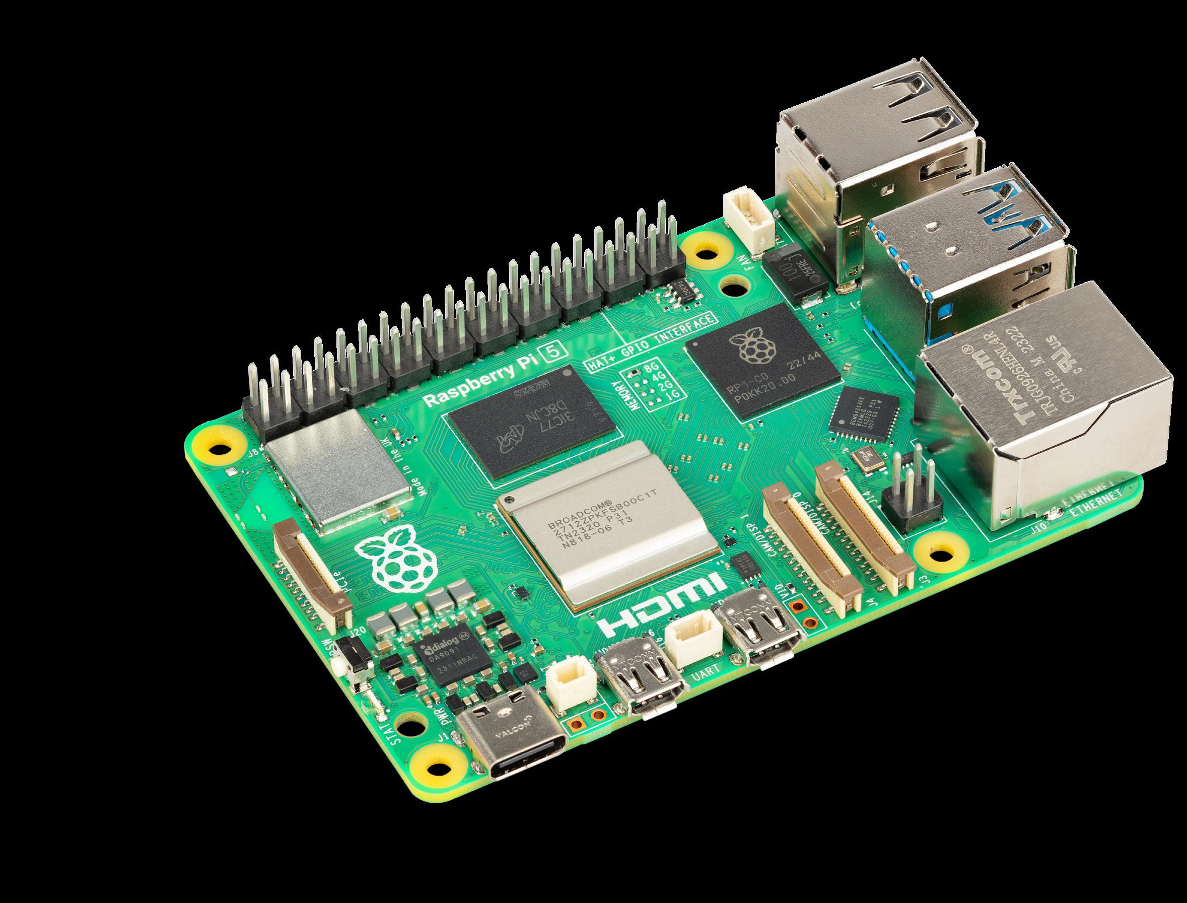
Key features of the new Raspberry Pi 5 include:
• 2.4GHz quad-core, 64-bit Arm Cortex-A76 CPU, with 512KB L2 caches and a 2MB shared L3 cache
• VideoCore VII GPU
LPDDR4X-4267 SDRAM
• 2.4 GHz and 5.0 GHz 802.11ac Wi-Fi Bluetooth 5.0 / Bluetooth Low Energy (BLE)
• Micro SD card slot, with support for high-speed SDR104 mode
• 2 × USB 3.0 ports, supporting simultaneous 5Gbps operation and 2 × USB 2.0 ports Gigabit Ethernet, with PoE+ support (requires PoE+ HAT)
2 × 4 lane MIPI camera/display transceivers
• PCIe 2.0 x1 interface for fast peripherals 5V/5A DC power (PD enabled)
• Raspberry Pi standard 40-pin header
• Real-Time Clock (RTC), powered from external battery
• On-board power button
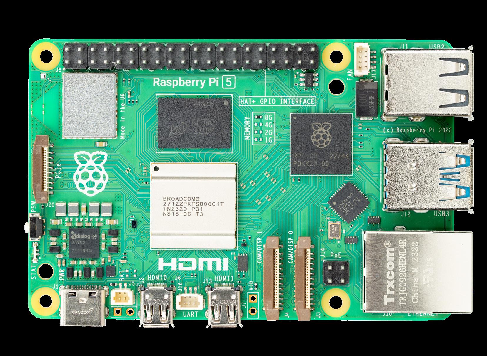
22 ELECTRONIC PRODUCTS & TECHNOLOGY / April 2024 EPT.CA
Photo: Raspberry Pi
ELECTRONICS MARKET
EPTECH 2024
EPTECH is back! Connecting you with the electronics market throughout Canada.
Eptech is an efficient table top show, which allows exhibitors to easily set up their display and showcase innovative products to OEM’s throughout Canada. Book today to to reserve a great position. Receive exclusive face-to-face networking opportunities with attendees including OEM’s, designers, engineers and project managers.
Exhibitors also have the opportunity to host on-site seminars to discuss new products and solutions for electronics projects.

TO REGISTER VISIT:
Eptech.ca
Toronto April 17
Quebec City May 7
Vancouver June 4
Montreal September 10
Calgary October 3
Mississauga October 22
CONNECT
LARGEST
TO CANADA’S
SCAN HERE!
Hammond has over 20 million dollars of in-stock inventory and over 16,000 unique product skus to choose from.


24 ELECTRONIC PRODUCTS & TECHNOLOGY / April 2024 EPT.CA Hammond Manufacturing | www.hammondmfg.com Hammond_EPandT_Magazine_23
ENCLOSURES
SMALL
extruded
and plastic enclosures
and configurations. RACK MOUNTING SOLUTIONS 19” racks, cabinets, and accessories for test & measurement, data communications and more. POWER DISTRIBUTION
and 20A heavy duty outlet strips for commercial/industrial, rack mount, and benchtop applications.
Diecast aluminum,
aluminum,
in thousands of sizes
15A
TRANSFORMERS
ELECTRICAL ENCLOSURES Junction, wall mount, and freestanding enclosures in painted steel, stainless steel, aluminum and non-metallic.
Low voltage power transformers, high-end audio transformers and chokes, medical grade isolation.
WE ARE IN-STOCK
