VOL. 27, NO. 4 Winter 2018
IN THIS ISSUE 3 From the Editor:
Ends and Beginnings
7 From the President:
Globalization Starting from Science
9 AiMES 2018, Cancun
ECS Meeting Highlights
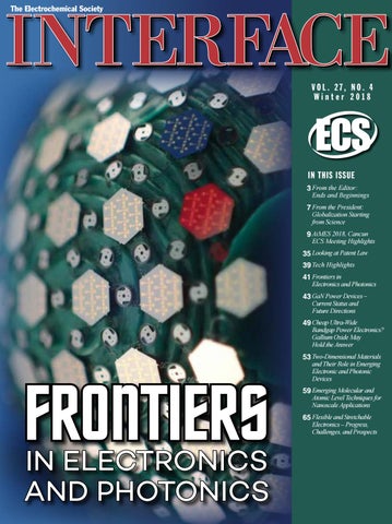
35 Looking at Patent Law 39 Tech Highlights 41 Frontiers in
Electronics and Photonics
43 GaN Power Devices – Current Status and Future Directions
49 Cheap Ultra-Wide
Bandgap Power Electronics? Gallium Oxide May Hold the Answer
53 Two-Dimensional Materials
Frontiers
in Electronics and Photonics
and Their Role in Emerging Electronic and Photonic Devices
59 Emerging Molecular and
Atomic Level Techniques for Nanoscale Applications
65 Flexible and Stretchable
Electronics – Progress, Challenges, and Prospects
ECS Monograph Series Special discount for ECS members!
MODERN
ELECTROPLATING
ElEctrochEmical PowEr SourcES Batteries, Fuel Cells, and Supercapacitors
FIFTH EDITION
Edited by
M O R D E C H AY S C H L E S I N G E R MIL AN PAUNOVIC
MOLECULAR MODELING OF
CORROSION PROCESSES Scientific Development and Engineering Applications EDITED BY
Christopher D. Taylor Philippe Marcus
Vladimir S. Bagotsky Alexander M. Skundin Yurij M. Volfkovich
SECOND EDITION
ATMOSPHERIC
CORROSION
Christofer Leygraf Inger Odnevall Wallinder Johan Tidblad Thomas Graedel
18 - 321712
Order your copy at www.electrochem.org
Have you made your list and checked it twice?
SANTA’S L
IST Merry Chris om youas iends r at
www.scribner.com
FROM THE Editor
B
Ends and Beginnings
y the time you read this, the end of 2018 will be upon us, as shocking as that is to my system. I anticipate it taking several months to stop typing “2018” in documents, as usual. The year has brought with it a lot of ends and beginnings. Personally, Heather and I have become empty nesters (although the house remains active with our two furry, four-legged whippet dog-children)—both an end and a beginning. Of probably more interest to you, this year The Electrochemical Society has made a major transition to new leadership, including Chris Jannuzzi becoming the executive director and CEO. Although badly handicapped by his selection of his favorite (American) football team (the New York Giants), Chris is passionate about the mission of ECS and is clear-eyed about the challenges we face both as a scientific society and a nonprofit scientific publisher. Closer to home, the ECS Publications Subcommittee inexplicably selected me as editor of Interface. At the Cancun meeting, I visited as many of the executive committees of the technical divisions as I could, with the notable exception of Industrial Electrochemistry and Electrochemical Engineering due to my inability to differentiate 7:00 am from 7:00 pm as a meeting start time, and that cannot be rationalized by the frightening availability of margaritas in the Moon Palace. At each meeting I was struck by the level of passion for their technical area as well as their willingness to contribute to the continued success of Interface. This deep commitment was also displayed at the Interface Advisory Board meeting, at which we discussed how to make the future of Interface consistent with its past successes. Allow me to let you in on some of the plans. Beginning in 2019, Interface will be published on a true quarterly basis. The sharp-eyed amongst you will have noticed that in the past, the summer and fall issues were published only two months apart. Historically, this timing was the result of the need for Interface to contain the meeting program for the fall meeting of ECS. Due to the amazing popularity of something called “the Internet,” the meeting program is now available electronically far earlier and is much more accessible through the ECS Mobile phone app. Thus we can become a true quarterly publication, with publication dates at the end of March, June, September, and December. With the help of ECS Director of Publications Beth Craanen and Interface Managing Editor Annie Goedkoop, we have developed a series of processes to help the guest editors and authors produce the kind of technical articles that readers appreciate—ones that enlighten us on the exciting developments in a scientific area and make those of us outside that area question our career choices. Spoiler alert: this issue’s technical articles on power electronics, 2D materials, ultra-thin layer processing, and flexible electronics from the ECS Electronics and Photonics Division do just that. Other changes are afoot as well. In case you missed it, all Interface technical articles now have their very own DOI number, making them easier to cite and find, as they are being indexed by Big Brother. The Looking at Patent Law series will continue with the use of case studies tied to the technical area of each issue in order to allow E. J. Taylor and Maria Inman to better educate the legally challenged amongst us. Probably due to bad karma accumulated in a previous life, Dennis Hess, editor of the ECS Journal of Solid State Science and Technology, had the great misfortune of sitting next to me on what was surely the longest two-hour flight of his life from Cancun to Atlanta. During our wide-ranging conversation, we discussed ways to better connect Interface with both of the Society’s journals. These include developing more technical perspective articles from articles in Interface, doing more with ECS Classics, and expanding coverage of other historical aspects of ECS. Finally, I would like Interface to be a place where we learn more about each other and celebrate each other’s accomplishments. So when good things happen to you or your colleagues, let me know (see email address below). It could be a promotion, a large grant, a student award, or finally being granted parole. I can’t promise that all news items will be included, but I have asked all of the technical division executive committees to pass on news of their members, so when they reach out, don’t be bashful. Until next time, be safe and happy.
Rob Kelly Editor rgk6y@virginia.edu https://orcid.org/0000-0002-7354-0978
The Electrochemical Society Interface • Winter 2018 • www.electrochem.org
Published by: The Electrochemical Society (ECS) 65 South Main Street Pennington, NJ 08534-2839, USA Tel 609.737.1902, Fax 609.737.2743 www.electrochem.org Editor: Rob Kelly, rgk6y@virginia.edu Guest Editor: Jennifer Hite, Jennifer.Hite@nrl.navy.mil Contributing Editors: Donald Pile, Donald.Pile@gmail. com; Alice Suroviec, asuroviec@berry.edu Managing Editor: Annie Goedkoop, Annie.Goedkoop@electrochem.org Print Production Manager: Dinia Agrawala, interface@electrochem.org Advertising Manager: Ashley Moran, Ashley.Moran@electrochem.org Staff Contributors: Marcelle Austin, Annie Goedkoop, Ngoc Le, John Lewis, Jennifer Ortiz, Shannon Reed, Andrew Ryan. Advisory Board: Brett Lucht (Battery), Dev Chidambaram (Corrosion), Durga Misra (Dielectric Science and Technology), Philippe Vereecken (Electrodeposition), Jennifer Hite (Electronics and Photonics), A. Manivannan (Energy Technology), Sean Bishop (High-Temperature Energy, Materials, & Processes), John Weidner (Industrial Electrochemistry and Electrochemical Engineering), Uwe Happek (Luminescence and Display Materials), Slava Rotkin (Nanocarbons), Jim Burgess (Organic and Biological Electrochemistry), Andrew Hillier (Physical and Analytical Electrochemistry), Nianqiang (Nick) Wu (Sensor) Director of Publications: Beth Craanen, Beth.Craanen@electrochem.org Publications Subcommittee Chair: Stefan De Gendt Society Officers: : Yue Kuo, President; Christina Bock, Senior Vice President; Stefan De Gendt, 2nd Vice President; Eric Wachsman, 3rd Vice President; James Fenton, Secretary; Gessie Brisard, Treasurer; Christopher J. Jannuzzi, Executive Director Statements and opinions given in The Electrochemical Society Interface are those of the contributors, and ECS assumes no responsibility for them. Authorization to photocopy any article for internal or personal use beyond the fair use provisions of the Copyright Act of 1976 is granted by The Electrochemical Society to libraries and other users registered with the Copyright Clearance Center (CCC). Copying for other than internal or personal use without express permission of ECS is prohibited. The CCC Code for The Electrochemical Society Interface is 1064-8208/92. Canada Post: Publications Mail Agreement #40612608 Canada Returns to be sent to: Pitney Bowes International, P.O. Box 25542, London, ON N6C 6B2 ISSN : Print: 1064-8208
Online: 1944-8783
The Electrochemical Society Interface is published quarterly by The Electrochemical Society (ECS), at 65 South Main Street, Pennington, NJ 08534-2839 USA. Subscription to members as part of membership service; subscription to nonmembers is available; see the ECS website. Single copies $10.00 to members; $19.00 to nonmembers. © Copyright 2018 by The Electrochemical Society. Periodicals postage paid at Pennington, New Jersey, and at additional mailing offices. POSTMASTER: Send address changes to The Electrochemical Society, 65 South Main Street, Pennington, NJ 08534-2839. The Electrochemical Society is an educational, nonprofit 501(c)(3) organization with more than 8,500 scientists and engineers in over 75 countries worldwide who hold individual membership. Founded in 1902, the Society has a long tradition in advancing the theory and practice of electrochemical and solid state science by dissemination of information through its publications and international meetings. 3 All recycled paper. Printed in USA.
Rapid, High-Current Pulsing & Superior, Low-Impedance EIS Reference 30K Booster Nobody is faster Distortion-free, rapid pulsing for charge and discharge
30 A Pulse on a 5 mOhm cell
Nobody goes lower Up to 30A @ 20V, EIS to 300 kHz
200 nOhm Shorted Lead Curve 20 A rms, 0.9 m cell cable
www.gamry.com
41 43
Frontiers in Electronics and Photonics by Jennifer K. Hite GaN Power Devices – Current Status and Future Directions by Travis J. Anderson, Srabanti Chowdhury, Ozgur Aktas, Michal Bockowski, and Jennifer K. Hite
49 53
Cheap Ultra-Wide Bandgap Power Electronics? Gallium Oxide May Hold the Answer by Marko J. Tadjer
59
Emerging Molecular and Atomic Level Techniques for Nanoscale Applications by Alain E. Kaloyeros, Jonathan Goff, and Barry Arkles
65
Two-Dimensional Materials and Their Role in Emerging Electronic and Photonic Devices by Colm O’Dwyer, Lee A. Walsh, Farzan Gity, Shubhadeep Bhattacharjee, and Paul K. Hurley
Flexible and Stretchable Electronics – Progress, Challenges, and Prospects by Muhammad M. Hussain, Zhenqiang (Jack) Ma, and Sohail F. Shaikh
The Electrochemical Society Interface • Winter 2018 • www.electrochem.org
Vol. 27, No. 4 Winter 2018
the Editor: 3 From Ends and Beginnings the President: 7 From Globalization Starting from Science
2018, Cancun 9 AiMES ECS Meeting Highlights
16 Candidates for Society Office 18 Society News 32 People News 35 Looking at Patent Law 39 Tech Highlights 70 Section News 72 Awards Program 74 New Members 2018 Summer 78 ECS Fellowship Reports 87 Student News ECS Meeting 93 236th Atlanta, GA Call for Papers
On the Cover: Fully spherical stretchable silicon photodiodes array for simultaneous 360 imaging. See article on page 65. (Reprinted from Appl. Phys. Lett., 113, 134101 (2018), with the permission of AIP Publishing.) Photo: Galo Torres Sevilla Cover design by Dinia Agrawala. 5
The
Quartz Crystal Microbalance Solution
QCM200… $2995 (US list) • • • • •
Measures and displays frequency and resistance Nanogram sensitivity Stand-alone operation and computer control Analog outputs Windows / Mac software included
With the QCM200, measuring the mass and viscoelasticity of a film or liquid is now easy. The QCM comes complete with control / oscillator electronics, crystal holder, crystals and software. Operated either manually or under computer control, the QCM200 is ideal for a wide range of applications including chemical and biological sensor development, thin film analysis and electrochemistry. Call or visit our web site for full details.
Stanford Research Systems
1290-D Reamwood Ave., Sunnyvale, CA 94089 • e-mail: info@thinkSRS.com Phone (408) 744-9040 • Fax (408) 744-9049 • www.thinkSRS.com
From The President
Globalization Starting from Science
G
obalization is probably one of the most-discussed topics of the last decade. It impacts almost all facets of our society, from the economy and culture to education and politics. The goal of globalization is to increase mutual understanding among people who come from different cultures, countries, regions, or religions as a means of fostering harmony across civilizations, improving people’s lives, and eventually reaching peace. The globalization process is analogous to a common phenomenon in chemical reactions— approaching equilibrium. Only in this case, it is human beings, not chemicals, that are involved in the process. In actuality, globalization started a long time ago. More than 2,000 years ago, for instance, there were frequent communications between the two largest empires on earth—the Roman Empire and the Han dynasty. These two distinct civilizations exchanged goods, services, and wealth on a routine basis. This process expanded to include other societies— and continued uninterrupted— independent of changes in rule. Over 1,000 years later, more frequent communications were carried out by means of new and enhanced routes. As long-distance sailing technology improved, globalization took to the seas. Though initially driven by economic incentive, globalization came to also influence other aspects of life, such as the arts, food, language, religion, and social and political systems. Many of the changes spurred by globalization were slow and irreversible. Today, globalization moves at an unprecedented speed, thanks to the development of the internet and advances in land, sea, and air transportation. Moreover, the focus of globalization has expanded beyond its economic origin (i.e., to education, philosophy, principles, laws, and politics). In spite of many contrasting opinions on how globalization should be carried out, it is generally recognized that all activities should
be equal, impartial, and fair—independent of race, gender, religion, nationality, or region. However, throughout the span of history, cultures have developed very different views on how globalization should be addressed. Furthermore, it takes a very long time (e.g., thousands of years) in order to achieve the goals of globalization. On the other hand, the goals of globalization have basically been achieved in the science field. ECS is probably one of the best examples on this topic—for a variety of reasons. For example, the Society’s over 8,000 members come from 80 countries across the globe, and the composition of the ECS Board of Directors clearly reflects the diversity of the membership. No one is denied membership due to reasons of race, gender, nationality, or related factors. No one is barred from attending or presenting papers at ECS meetings for nonscientific reasons. Likewise, the publication of papers in ECS journals or ECS Transactions is solely dependent on the technical content and quality of submissions; considerations of authors’ personal backgrounds have no influence upon editorial decisions. The stated mission of The Electrochemical Society is “to advance theory and practice at the forefront of electrochemical and solid state science and technology, and allied subjects.” ECS’s success as a global organization can be attributed to what is at its core—science. Independent of economic or political forces, when a subject is discussed based on science, the answer is clear and unambiguous. The technical content and activities of ECS are based entirely on science. This is why ECS has lasted for so many years and is still going strong. Papers published in the Journal of The Electrochemical Society have a 10-year citation lifetime—longer than those in most other journals. This is an outstanding testament to the Society’s longevity. In sum, ECS is a prime example of successful globalization because its content and activities are based on scientific principles that are recognized worldwide.
Yue Kuo ECS President president@electrochem.org https://orcid.org/0000-0003-2757-1842
The Electrochemical Society Interface • Winter 2018 • www.electrochem.org
7
BluRev RDE:
Straight to the Point Accurate: ± 1 rpm over the whole rotational range (1,000 to 10,000 rpm) Displays both target and actual rates of rotation Simple to use
ergonomic design
fits standard glassware
Robust: gas entry port to safeguard against corrosion Controlled by EC-Lab or independently Determine kinetic parameters directly via: Standard analysis: Levich, Koutecký-Levich Innovative analysis: *Winf in Z Fit
You, BluRev RDE, and Winf: A perfect fit *Winf is a new impedance element to model convective diffusion. Contrary to the Wδ element, it does not follow the Nernst hypothesis and considers that the concentration perturbation also occurs outside of the diffusion layer. The diffusion coefficient of the redox species is directly calculated and the quality of the fit is improved. 8
www.bio-logic.us
The Electrochemical Society Interface • Winter 2018 • www.electrochem.org
Cancun Mexico September 30-October 4, 2018 M oon Pa la ce R e s ort
A
Highlights from AiMES 2018
lmost 2,000 people attended the Americas International Meeting on Electrochemistry and Solid State Science (AiMES 2018) in Cancun, Mexico, a joint conference of the 234th Meeting of The Electrochemical Society (ECS), the XXXIII Congreso de la Sociedad Mexicana de Electroquímica (SMEQ), and the 11th Meeting of the Mexico Section of The Electrochemical Society, with the technical cosponsorship of the Sociedade Brasileira de Eletroquímica e Eletroanalítica (SBEE), the Sociedad Iberoamericana de Electroquímica (SIBAE), and the Asociación Colombiana de Electroquímica (ACEQ). Participants could choose from 53 symposia, with over 1,700 oral talks and nearly 500 posters, of which almost 600 were student presentations.
Opening Reception
AiMES 2018 was held at the all-inclusive Moon Palace Resort in Cancun.
Plenary Session
AiMES kicked off with the opening reception on the first night of the meeting. Along the shoreline of the Caribbean Sea, with the sandy beach just steps away, attendees gathered for a night of food, drinks, and great conversation on the Moonlight Terrace of the all-inclusive Moon Palace Resort. People chatted over beers, guacamole and chips, seafood, tacos, and more. Some guests arrived via golf carts, a service offered graciously by the Moon Palace staff. Dark blue skies and gusts of tropical winds crept in throughout the course of the night, eventually breaking out into a downpour. Although the event was rained out, the party was not. Guests moved to a bar inside the hotel and ushered in the week with optimism and laughs.
SMEQ President Ricardo Orozco-Cruz presented the opening remarks at AiMES 2018, calling the meeting to order and welcoming attendees to Cancun.
Attendees gathered to network and enjoy food and drinks at the meeting’s opening reception.
Ricardo Orozco-Cruz, president of the Sociedad Mexicana de Electroquímica (SMEQ), welcomed attendees to the meeting during Monday evening’s plenary session, which wrapped up the day’s technical sessions, honored award winners, and featured a highly anticipated lecture. “On behalf of SMEQ and ECS, it is my pleasure to call this meeting to order,” announced Orozco-Cruz. “Welcome to Cancun!” “With 53 topical symposia, 2,100 abstracts, almost 500 invited talks, and nearly 600 student presentations,” Orozco-Cruz continued, “I’m proud to be part of the first Americas International Meeting on Electrochemistry and Solid State Science. We call it AiMES.” Orozco-Cruz explained that the joint meeting “formalizes our long-standing collaboration with the goal of enabling our research in the Americas.” (continued on next page)
The Electrochemical Society Interface • Winter 2018 • www.electrochem.org
9
(continued from previous page)
ECS President Yue Kuo recognized the Society’s partners, award winners, and newly inducted fellows during the plenary session.
ECS President Yue Kuo then took the stage, thanking OrozcoCruz. Kuo acknowledged the success of their partnership, as well as others’ contributions to the Society’s advances. Kuo thanked past ECS president Johna Leddy and past ECS treasurer E. J. Taylor for their years of distinguished service, which contributed to the continued growth and success of the Society. He also thanked the Society’s institutional members for supporting scientific education, sustainability, and innovation. “They are truly partners in advancing our science,” said Kuo. He went on to honor award winners and the Society’s 2018 Class of Fellows. Kuo ended by emphasizing the importance of International Open Access Week. “As ECS did the last three years, we are celebrating by giving the world a preview of what complete open access will look like. From October 22 through October 28, we are taking down the paywall to the ECS Digital Library,” said Kuo. “Over 141,000 articles and abstracts will be freely available to anyone who wants to read them. We hope to make this the norm in the future through our Free the Science initiative.”
Plenary Lecture Luis A. Godínez, a researcher at the Centro de Investigación y Desarrollo Tecnológico en Electroquímica, was the meeting’s plenary speaker. His lecture, “Electro- and Photo-Electro-Chemical Generation of the Fenton Reagent. Some Approaches for the Development of Electrochemical Based Advanced Oxidation Processes for Water Treatment,” focused on water management and the technological potential of the electro-Fenton approach—water management being a complicated issue for Mexico and other countries. Godinez described the great need for inexpensive, efficient, and accessible water treatment for disinfection of water for the 2.6 billion
Luis A. Godínez, a researcher at the Centro de Investigación y Desarrollo Tecnológico en Electroquímica, delivered the meeting’s plenary lecture. 10
people worldwide without access to sanitation services. He described the power of the Fenton reagent (hydrogen peroxide and ferrous ion) to disinfect contaminated water. It is nonspecific (therefore broadly effective) and has a high oxidizing power. The challenges in use at scale are the need for the solution to be acidic and the safety and cost issues surrounding the handling of hydrogen peroxide in large volumes and relevant concentrations. The use of the controlled electrochemical reduction of dissolved oxygen via the two-electron path to produce the hydrogen peroxide needed allows that component to be produced on demand. By adding UV light, photoassistance can be used to create holes, leading to the production of both hydroxyl radicals and regeneration of the ferrous ion (which is oxidized by the peroxide in the process of production of hydroxyl radicals). Two applications of the electro-Fenton process were described. The first involved the regeneration of activated carbon. This activated carbon is used worldwide as an inexpensive filtration medium, but the standard regeneration processes involve high-energy expenditures and the need to remove the material from the packaging. That standard regeneration process degrades the activated carbon, thus limiting the useful life. Using the electro-Fenton process, the activated carbon can be regenerated in place, and the process is less expensive, and, equally important, more gentle to the activated carbon. The process involves three compartments in series, with two of them packed with cation exchange resin. The hydroxyl radicals are produced in situ and react with the pollutants on the activated carbon serving as a cathode. This solution is then passed through the second cation exchange resin which removes the ferric cation (for later regeneration) and the acid (for later neutralization). The second example involved the creation of a sanitation service for human wastewater using the electro-Fenton process. Godinez showed that the process had excellent inactivation efficiency of Helminth eggs (HE) from the parasite Ascaris lumbicoides. These eggs are difficult to deactivate as they have protective external membranes. For example, the use of hypochlorite solution for two hours reduced the number of HE by only 60%. The electro-Fenton process reduced the number by 92% and altered the shape of the eggs, indicative of permanent damage to the external membranes. Godinez and his team have been able to engineer the reactor in such a way that it can be powered by solar cells.
Electrochemical Energy Summit The 8th Annual Electrochemical Energy Summit (E2S) was held during AiMES 2018. Its theme was “Sustainable and Responsible Supply of Energy Storage Materials, Components, and Devices.” The summit consisted of invited speakers, posters, and a panel discussion featuring experts along the entire processing chain of energy storage, which includes mining as well as materials, components, and device manufacturing and recycling. The summit was moderated by Luis A. Diaz Aldana (Idaho National Laboratory) and Marca Doeff (Lawrence Berkeley National Laboratory) and featured the following invited talks: • “Supply Chain Considerations for Lithium-Ion Battery Materials,” by E. A. Olivetti (MIT) and G. Ceder (University of California, Berkeley) • “Material Criticality and Energy Storage Materials,” by R. Eggert (Colorado School of Mines) • “The Advantages of the Nemaska Electrochemical Process to Directly Synthesize High Purity Lithium Hydroxide,” by J. F. Magnan (Nemaska Lithium Inc.) • “Present Status and Future R&D Needs for Batteries for Vehicle and Grid Applications,” by V. Srinivasan (Argonne National Laboratory) • “Direct Recycling of Lithium-Ion Batteries,” by S. E. Sloop (OnTo Technology, LLC), W. Xu (Oregon State University), M. M. Lerner (Oregon State University), J. Kim (Spear Power Systems, LLC), and M. Lee (Spear Power Systems, LLC) The Electrochemical Society Interface • Winter 2018 • www.electrochem.org
ECS Data Science Showcase AiMES 2018 featured the first ECS Data Science Showcase, an event that highlighted new electrochemical and solid state research and the open-source software and datasets that underpin the work. The event was led by the University of Washington team that brought you ECS Data Sciences Hack Day (fall 2017) and ECS Data Sciences Hack Week (spring 2018): Daniel Schwartz, the BoeingSutter Professor of Chemical Engineering and director of the Clean Energy Institute at the University of Washington; David Beck, senior data scientist with the eSciences Institute at the University of Washington and associate director of the NSF Data Intensive Research Enabling CleanTech PhD training program; and Matthew Murbach, past president of the ECS University of Washington Student Chapter and advanced data sciences PhD trainee. Talks were complemented by demonstrations on how others can access, use, modify, and improve the open-source tools and data associated with research projects.
Hatem Amin, from the University of Oxford in New York, echoed the same sentiment, saying the student mixer presented the opportunity to meet students he would have never been able to meet at his university or campus alone. Oliver Rodriguez, from the University of Southampton, said that for him, the mixer was a great way to catch up with students he had met in the past. All agreed the mixer provided a beneficial platform for young professionals to meet or reunite. “They’re all my age, so we share a perspective on many things that I may not share with some of the older members of the Society,” said Ian VonWald, from the University of North Carolina at Chapel Hill. “We’re all going through the same sort of existential crises—things like what kind of jobs are we going to have, are we going to have jobs—all these kinds of things.” He concluded by saying that he finds it easier to meet people at the ECS student mixer than at other conferences he has been to. Each attendee of the mixer received a bright yellow shirt that read “AiMES 2018 Student Mixer” as a keepsake of the event.
Attendees of the student mixer showcased their souvenir t-shirts. The ECS Data Sciences Showcase featured talks and demonstrations on open-source tools and datasets.
Student Mixer Young researchers enjoyed the student mixer held on the second night of AiMES—an event created as a platform for peers and earlycareer professionals in the field to mix and mingle in a relaxed setting. Guests were greeted with a buffet of food, desserts, and drinks, which they enjoyed as they chatted throughout the night. Iqra Reyaz Hamdani, from the Indian Institute of Technology Delhi, said that for her, having the opportunity to connect with people from all around the world was a highlight of the event.
Young researchers mingled while enjoying a buffet of food, desserts, and drinks at the meeting’s student mixer.
Award Highlights ECS is proud to report that many of its members were recognized with awards at AiMES 2018—both during the plenary and throughout the week. The ECS Edward Goodrich Acheson Award was presented to past ECS president Tetsuya Osaka, who serves as senior research professor and emeritus director of the Institute for Research Organization for Nano & Life Innovation, and as professor emeritus of the faculty of science and engineering at Waseda University in Tokyo, Japan. The award recognizes distinguished contributions to the advancement of the objects, purposes, and activities of ECS. (continued on next page)
Tetsuya Osaka (left), recipient of the ECS Edward Goodrich Acheson Award, with ECS President Yue Kuo (right).
The Electrochemical Society Interface • Winter 2018 • www.electrochem.org
11
(continued from previous page)
Osaka has also served as president of the Magnetics Society of Japan, president of the Electrochemical Society of Japan, and president of the Japan Institute of Electronic Packaging. He has made significant contributions to the advancement of electrochemical science and technology, particularly in the areas of electrodeposition, magnetic device fabrication, energy conversion, biosensors, and electrochemical nanotechnology. The ECS Charles W. Tobias Young Investigator Award was presented to Michael Arnold for his work “Overcoming the Materials Science Challenges to Nanocarbon Electronics.” The award recognizes outstanding scientific or engineering work in fundamental or applied electrochemistry or solid state science and technology. Arnold, a professor in the Materials Science and Engineering Department at the University of Wisconsin-Madison, says his focus is on two applications—first, to make new semiconductors that are better than silicon to make computer chips faster and use less power, so the battery lasts longer, and second, to create biosensors that can
Michael Arnold, recipient of the ECS Charles W. Tobias Young Investigator Award.
measure concentrations of proteins in blood by using a semiconductor. “I’m trying to make new semiconductors from carbon that could improve all of those applications,” said Arnold. In reference to the award, he said, “It’s fantastic recognition, not only just of my efforts but my students’ efforts. I mean, the students are the ones in my group doing the work, so it makes me proud to receive the reward, but it’s really pride in my group.” The ECS Norman Hackerman Young Author Award was presented to Raymond Smith for his paper “Multiphase Porous Electrode Theory,” published in the Journal of The Electrochemical Society (JES). The award recognizes the best paper published by young authors in JES in the previous year. Smith, who holds a PhD in chemical engineering from MIT and works as a senior engineer at Tesla, said he was blown away when he heard he was nominated for the award. His paper focuses on battery modeling—understanding exactly what is going on inside of a cell or a battery to improve the design and make it more effective.
Raymond Smith, recipient of the ECS Norman Hackerman Young Author Award. 12
His paper aimed to unify work that his team and other teams have done in the field in order to highlight connections that weren't obvious before. “I hope it provides a useful resource that shows similarities between works, that maybe people didn't understand were the same before,” said Smith. The ECS Bruce Deal & Andy Grove Young Author Award was presented to Shihyun Ahn for his paper “Temperature-Dependent Characteristics of Ni/Au and Pt/Au Schottky Diodes on β-Ga2O3,” published in the ECS Journal of Solid State Science and Technology (JSS). The award, named for two pioneers in the semiconductor industry, recognizes the best paper published by young authors in JSS in the previous year. Ahn, who holds a PhD in chemical engineering from the University of Florida, is currently working in the Ultraviolet Product Development Department at Seoul Viosys in Korea. In May, ECS teamed up with Amazon to create Amazon Catalyst at ECS. The goal of the program is to find solutions that make life easier, healthier, more sustainable, and more enjoyable. To encourage and support researchers, Amazon Catalyst committed up to $100,000 to help fund the selected proposals. The award recipients, award amounts, and project titles are listed below. • Sampath Kommandur and Aravindh Rajan ($1,600), “Active Control of Heat Flor in Quantum Computing Applications through Piezoelectric Induced Mechanical Strain” • Mohammadreza Nazemi ($25,000), “Using Nanotechnology for Electrosynthesis of Nitrogen-Based Fertilizer under Ambient Conditions” • Rajib Das ($25,000), “Carbon Catalysts for Cost-Efficient Hydrogen Production in PEM Electolyzers” • Jennifer Schaefer and Peng He ($36,000), “MagnesiumPolysulfied Flow Batteries” A progress report on each of these projects will be presented next year at the 236th ECS Meeting in Atlanta, GA. The ECS Toyota Young Investigator Fellowship was awarded to two individuals: Kimberly See, from the California Institute of Technology, and Iryna Zenyuk, from the University of California, Irvine. Each will receive $50,000 to pursue projects in green energy technology. Christina Bock, senior vice president of ECS, assisted with the introduction of the 2018 Class of Fellows. These 14 members are recognized for their contributions to the advancement and leadership in electrochemical and solid state science and technology, and for active participation in the affairs of ECS. • Sheikh A. Akbar—for sustained high-quality contributions to the field of high-temperature sensors, education and training of students, and for active participation in leadership activities in the field of sensors. • Yi Cui—for outstanding contribution to nanotechnology and electrochemistry, particularly in energy storage. • Jan Fransaer—for demonstrating world-class and high-quality scientific leadership in electrochemistry (fundamental and applied). • Turgut M. Gür—for pioneering contributions to the development of carbon fuel cells for clean energy from fossil fuels and spontaneous hydrogen coproduction, high-temperature electrocatalysis and electrosynthesis of industrially important reactions, surface and interface engineered thin film solid oxide fuel cells, and solid state ionic tools for fundamental materials research. • Pawel J. Kulesza—for longstanding contributions and development of original approaches to fabrication, fundamental understanding, and utilization of highly functionalized and active electrochemical interfaces. • Stuart Licht—for innovative work in energy storage, solar energy capture, and the development of a novel, sustainable means of producing commercial materials without greenhouse gas production. The Electrochemical Society Interface • Winter 2018 • www.electrochem.org
• Y. Shirley Meng—for impactful contributions to battery research and the leadership and mentoring of students and young researchers. • Junichiro Mizusaki—for extensive seminal contributions to the fundamental understanding of the reactions and the thermodynamic and electrochemical properties of materials in electrochemical devices and worldwide activities in the field of electrochemistry and solid state ionics. • Venkat R. Subramanian—for outstanding contributions to the computational science and engineering that underpins safe and economical battery design and control. • Jay Switzer—for pioneering and sustained contributions to the electrodeposition of ceramic films and epitaxial nanostructures and the relentless promotion of electrochemistry to the scientific community. • Tomás Torres—for contributions toward the understanding of the chemistry of phthalocyanine-carbon nanostructures conjugates. • Hiroyuki Uchida—for outstanding contributions in the areas of SOFC materials development, electrocatalysis, catalyst synthesis and characterization for low-temperature fuel cells and electrolyzers, and the design of electrodes for fuel cells and electrolyzers, as well as his fundamental studies on electrode reactions and degradation mechanisms. • Sannakaisa Virtanen—for exceptional contributions to the field of corrosion, particularly in the areas of protective passive films and biocorrosion, and for sustained leadership in the field. • Adam Z. Weber—for contributions to the understanding of transport phenomena in fuel cells and related electrochemical devices. The ECS Outstanding Student Chapter Award was presented to the ECS University of Washington Student Chapter. The ECS Chapter of Excellence Awards were presented to the ECS Lewis University Student Chapter and the ECS University of Virginia Student Chapter.
There were 16 division and section awards presented over the course of the meeting. • The ECS Battery Division Research Award was presented to Kang Xu of the U.S. Army Research Laboratory. • The ECS Battery Division Technology Award was presented to Feng Pan of Peking University. • The ECS Battery Division Technology Award was presented to Yongyao Xia of Fudan University. • The ECS Battery Division Postdoctoral Associate Research Award sponsored by MTI Corporation and the Jiang Family Foundation was presented to Haodong Liu of the University of California, San Diego. • The ECS Battery Division Postdoctoral Associate Research Award sponsored by MTI Corporation and the Jiang Family Foundation was presented to David Bock of Brookhaven National Laboratory. • The ECS Battery Division Student Research Award sponsored by Mercedes-Benz Research & Development was presented to Fudong Han of the University of Maryland, College Park. • The ECS Battery Division Student Research Award sponsored by Mercedes-Benz Research & Development was presented to Steven Lacey of the University of Maryland. • The ECS Corrosion Division H. H. Uhlig Award was presented to Rudolph G. Buchheit of the University of Kentucky. • The ECS Corrosion Division Morris Cohen Graduate Student Award was presented to Rebecca Schaller of the University of British Columbia. • The ECS Electrodeposition Division Research Award was presented to Nosang Vincent Myung of the University of California, Riverside. • The ECS Electrodeposition Division Early Career Investigator Award was presented to Jon Ustarroz of the Vrije Universiteit Brussel. (continued on next page)
ECS 2018 Class of Fellows—front row (left to right): Sheikh A. Akbar, Turgut M. Gür, Y. Shirley Meng, ECS President Yue Kuo, Sannakaisa Virtanen, and Junichiro Mizusaki; back row (left to right): Jay Switzer, Jan Fransaer, Pawel J. Kulesza, Adam Z. Weber, and Hiroyuki Uchida. Not pictured: Yi Cui, Stuart Licht, Venkat R. Subramanian, and Tomás Torres. The Electrochemical Society Interface • Winter 2018 • www.electrochem.org
13
(continued from previous page)
• The ECS High-Temperature Energy, Materials, & Processes Division Outstanding Achievement Award was presented to Meilin Liu of the Georgia Institute of Technology. • The ECS Luminescence and Display Materials Division Centennial Outstanding Achievement Award was presented to Pieter Dorenbos of the Technical University of Delft. • The ECS Physical and Analytical Electrochemistry Division Max Bredig Award in Molten Salt and Ionic Liquid Chemistry was presented to Robin D. Rogers of The University of Alabama. • The ECS Sensor Division Outstanding Achievement Award was presented to Joseph Wang of the University of California, San Diego. • The ECS Europe Section Alessandro Volta Medal was presented to Wolfgang Schuhmann of Ruhr-Universität Bochum.
Z01 General Student Poster Session There were more than 80 student posters submitted to the Z01 General Student Poster Session at AiMES 2018. The recipients of the best student poster awards for AiMES 2018 are listed below. • Aranzazu Cermona Orbezo, The University of Manchester, “Flow-Electrode Capacitive Deionization (FCDI) Using Suspensions of 2D Materials as Electrodes” • Ashwin Ramanujam, Ohio University, “Rapid Electrochemical Detection of Escherichia coli Using a Rotating Disc Electrode” • Jeffrey Kowalski, Joint Center for Energy Storage Research, “Systematic Development of Positive Active Materials for Nonaqueous Redox Flow Batteries Using Phenothiazine as a Learning Platform” • Garrett Huang, Georgia Institute of Technology, “Advanced Anion Conducting Multiblock Copolymer Membranes with Hydrocarbon Backbones” • Ayano Ohama, Ochanomizu University, “Pre-Treatment Effects on Electrochemical Lithium Deposition/Dissolution Processes Studied by Electrochemical Quartz Crystal Microbalance” • Hafis Pratama Rendra Graha, Tokyo Institute of Technology, “Development of Highly Conductive and Highly Durable AllAromatic Anion Exchange Membranes by Using Thermally Convertible Precursor Polymer”
Recipients of the best student poster awards at AiMES 2018 (left to right): Aranzazu Cermona Orbezo, Jeffrey Kowalski, Ayano Ohama, and Hafis Pratama Rendra Graha. Not pictured: Ashwin Ramanujam and Garrett Huang.
14
The student poster awards acknowledge the quality and thoroughness of the candidates’ work, the originality and independence of their contributions, the significance and timeliness of the research results, and the depth of understanding of research topics and their relationships to ECS fields of interest. Shova Neupane, from the University of Hasselt in Belgium, was a poster presenter at the meeting. She said she enjoyed presenting her poster, as it allowed her the opportunity to receive feedback and answer questions regarding her work, “Initial Zinc Electrodeposition on Copper Studied by In-Situ AFM,” in a more intimate setting. “I noticed people held back on questions and comments during my talk,” Neupane explained. “The poster session makes it easier to have a conversation.” Raciel Jamies Lopez, from the Universidad Autónoma Metroplitana in Mexico, said he enjoyed the diversity the student poster session brings, “from international students to unique perspectives.” The following individuals served as organizers of the session: Venkat R. Subramanian (University of Washington), Kalpathy B. Sundaram (University of Central Florida), Vimal Chaitanya (New Mexico State University), Alice H. Suroviec (Berry College), Pallavi Pharkya (Lam Research Corporation), and Ricardo GalvànMartìnez (Universidad Veracruzana). The following individuals served as student poster judges: Krysti Knoche Gupta (University of Wisconsin Eau Claire), Lok-kum Tsui (University of New Mexico), David Rodriguez (Los Alamos National Laboratory), Eiji Tada (Tokyo Institute of Technology), Vito Di Noto (University of Padova), Brian Skinn (Faraday Technology, Inc.), Rod Borup (Los Alamos National Laboratory), Shrisudersan Jayaraman (Corning Inc.), Jeffrey Halpern (University of New Hampshire), Nikolay Dimitrov (Binghamton University), Eugeniusz Zych (Uniwersytet Wroclawski), and Bryan McCloskey (University of California, Berkeley). ECS thanks the organizers and judges for making the session a success.
Cena Baile Featuring drinks, food, and good conversation, the Cena Baile wrapped up AiMES with a sendoff only fitting for Cancun—a brief torrential downpour. Of course, that didn’t stop the festivities, beforehand or after. The night opened with live music and entertainment on the beachside Moonlight Terrace. Guests partook in the local cuisine while being invited to the dance floor. Although the event was cut short, attendees were able to enjoy an evening outdoors before heading off to other engagements.
AiMES wrapped up with the Cena Baile, a reception that featured food, drinks, and live entertainment.
The Electrochemical Society Interface • Winter 2018 • www.electrochem.org
Sponsors and Exhibitors Special thanks to the meeting’s sponsors and exhibitors, whose support and participation directly contributed to the success of the meeting. Thank you for developing the tools and equipment driving scientific advancement and for sharing your innovations with the ECS community.
Silver
make possible
Contributing American Elements
Save the Date 2020
237th ECS Meeting with the 18th International Meeting on Chemical Sensors (IMCS 2020)
Montreal, Canada May 10-15, 2020 Palais des Congrès de Montréal
The Electrochemical Society Interface • Winter 2018 • www.electrochem.org
15
candidates for for societ society y office office candidates The following are biographical sketches and candidacy statements of the nominated candidates for the annual election of ECS officers. The office not affected by this election is that of the secretary.
Candidate for President
Candidates for Vice President
Christina Bock is a senior research officer at the National Research Council of Canada (NRC), where she is a program technical and team leader for energy storage materials. She earned a doctoral degree from the University of Calgary in 1997, then joined NRC as an assistant research officer. During her career she made many contributions to electrochemistry, including the oxidation of organics for wastewater treatment, electrocatalysis for direct methanol and proton exchange membrane fuel cells, as well as hydrogen and oxygen evolution catalysts and supercapacitors. More recently, she has shifted her research and development efforts to batteries and lithium-extraction materials. She has co-supervised PhD students jointly with the University of Ottawa. Bock has published over 65 research articles (including invited contributions and review papers), five book chapters, one U.S. and Canadian patent and three patent applications, as well as over 20 technical reports. She has served on many committees for the evaluation of national laboratories and the funding of new university programs outside of Canada, and has served as an external expert for numerous PhD and master’s students’ theses. Bock has been an ECS member for over 25 years. She has served on numerous ECS committees, including the Ways and Means, Technical Affairs, and Education Committees, and has served as chair of the ECS Canada Section. She has served on the ECS Board of Directors, as chair of the Council of Sections, as chair of the Sponsorship Subcommittee, and as chair of the New Technology Subcommittee. She has also served as Society treasurer and vice president. She has presented many papers at ECS meetings, published in ECS journals, organized symposia, and chaired sessions. In 2011, Bock co-initiated the ECS Electrochemical Energy Summit series.
Turgut Gür is an adjunct professor of materials science and engineering at Stanford University, where he recently retired after a rewarding career that also included cofounding two and managing three major multidisciplinary teamand theme-based research centers on campus focused on energy and advanced materials. He also holds a visiting professor appointment from the Chinese University of Mining and Technology-Beijing. Gür is an ECS fellow and a recognized leader in high-temperature electrochemical energy research, materials, and technologies with 11 U.S. patents and more than 150 publications. He holds BS and MS degrees in chemical engineering from the Middle East Technical University in Ankara, Turkey, and three graduate degrees, including a PhD in materials science and engineering from Stanford University. He has been an active member of ECS since 1973 and has participated in top leadership positions in the Society. He was a member of the ECS Board of Directors and the chair of the ECS High-Temperature Energy, Materials, & Processes Division, and also served on several ECS advisory committees. He also co-organized more than a dozen ECS symposia and coedited 14 ECS Transactions volumes. Previously, he served on the board of the International Society for Solid State Ionics for 10 years, and was an associate editor of the Journal of the American Ceramic Society for 12 years.
Statement of Candidacy
Durga Misra is a professor in the Electrical and Computer Engineering Department at the New Jersey Institute of Technology (NJIT) in Newark, NJ. He served as the director of the Microelectronics Research Center at NJIT and currently is the director of the Nanoelectronics Device and Materials Characterization Laboratory there. He received his MS and PhD degrees, both in electrical engineering, from the University of Waterloo in Canada. He has edited and coedited 45 ECS Transactions and proceedings volumes and has over 300 publications in scientific journals and international conferences. He has presented more than 100 invited talks at many international conferences, universities, research laboratories, and industries all over the world. Misra has supervised 27 researchers who are currently employed at prestigious companies worldwide. Misra joined ECS in 1987 as a student member and has been an active member since 1989. He has organized numerous technical symposia and tutorials in interdisciplinary science and technology and in emerging technologies. He has served the ECS Dielectric Science and Technology and Electronics and Photonics Divisions as an executive committee member since late 1990s. He was elected chair of the Dielectric Science and Technology Division and revitalized that division during his tenure. His volunteer leadership extends to the ECS Technical Affairs Committee, Ways and Means Committee, Honors & Awards Committee, Individual Membership Committee, Interface Advisory Board, ECS Transactions Advisory Board, and Board of Directors (2008-2010). He is a fellow of The Electrochemical Society. Misra received the Dielectric Science and Technology Division Thomas D. Callinan Award and the Electronics and Photonics Division Award, both in 2013.
The grand challenges of the twentyfirst century in energy and environment fall squarely within our Society’s domain of interest. As ECS members, we have the fortunate opportunity and responsibility to tackle these pressing problems. If elected, I will lead ECS to serve as a science hub to impact sustainable solutions to these global challenges, for example, by creating opportunities for industry leaders and policymakers to join our biannual meetings and help bridge the gap between science, policy, and technology. I understand many of the challenges facing our Society. While we need to continuously provide an intellectually
ECS is a premier professional society in solid state science and technology and electrochemistry that has supported its members through knowledge dissemination and has enhanced our quality of life.
(continued on next page)
(continued on next page)
16
Statement of Candidacy
The Electrochemical Society Interface • Winter 2018 • www.electrochem.org
Turgut Gür (continued from previous page)
stimulating and scientifically vibrant home to our more than 8,000 dedicated members from nearly 80 countries, we also need to invest in students and young scientists from across the globe. If elected, I will help generate resources for young scientists to attend ECS meetings and make ECS their home. Expanding international and national student chapters will also help increase membership among young scientists. I applaud the Society’s Free the Science objective to disseminate knowledge freely through its high-quality journals. Realizing this noble cause, however, requires new income streams in order to compete with commercial publishers. If elected, I will work with ECS management and our members to minimize the financial burden of open access publishing. I will also seek like-minded professional societies to join forces with ECS to free the science.
Since I became an active member in 1973, ECS has been a home and an integral part of my professional life. I always valued the stimulating environment of ECS meetings, and felt fortunate to build many lasting friendships. It is indeed an honor to be considered for this position to further serve you. Durga Misra (continued from previous page)
Even though ECS has gone through several transformations over the years, it has to prepare itself for rapidly changing technology in the digital world. Therefore, our goal should be to expand the role of ECS to reach scientists and engineers all over the world through the Free the Science initiative with a result of increased ECS membership. Initiating strategic programs such as an industry forum in different fields through technology transfer will also directly
benefit the members and Society in general. Facilitating networking opportunities, especially for students and young, earlycareer researchers, with those who are more prominent through active mentorship programs can lead to higher productivity levels, higher levels of involvement with ECS, and greater member satisfaction. We need to continue with the high quality of publications with greater impact, vibrant meetings with the exchange of ideas between established and emerging research areas, relevant educational programs, and a strong reward system. As an active member of ECS for over three decades, I have a deep understanding of the new challenges that the Society encounters, especially in its membership, publications, conferences, and other professional activities. It is an honor for me to be nominated for the vice president position, and if elected, I plan to serve ECS and its membership to the best of my abilities.
Join our Hands-on seminars on Li-ion battery testing Learn more about: The latest devices and methods for battery testing Practical preparation and testing of Li-ion battery materials Electrode making from powder to sheet Testing with 3-electrode PAT-Cells Lifetime and CC-CV cycle tests Impedance measurements Cyclic voltammetry
Experimenting with the ECC-Opto-Std
Electrochemical in-situ / operando techniques with: ECC-Opto-Std (Optical test cell) PAT-Cell-Press (Gas analysis test cell) ECD-3 (Electrochemical Dilatometer) Moderator: Dr. Matthias Hahn Duration: Two days Location: Hamburg, Germany el-cell.com/services/hands-on-seminars
The Electrochemical Society Interface • Winter 2018 • www.electrochem.org
PAT-Cell assembly in the glovebox
17
socie t y ne ws First International Conference on 4D Materials and Systems Yonezawa l Japan
Sponsored by
August 26-30, 2018 Yamagata University
Highlights from 4DMS The First International Conference on 4D Materials and Systems (4DMS), sponsored by ECS, was held August 26-30, 2018, at the Faculty of Engineering at Yamagata University, which is located in the castle town of Yonezawa that was once home to the Uesugi clan, including the daimyō Uesugi Yozan. The conference had five parallel tracks: (1) Gel Symposium, (2) Flexible and Printed Electronics, (3) Material Processing, (4) Electrochemical Materials and Devices for Energy Conversion and Storage, and (5) Sensors and Systems. The meeting attracted 295 attendees, out of which 98 were students and 57 were international participants, with over 300 abstracts submitted. This international conference brought together engineers, medical professionals, clinicians, chemists, biologists, and physicists under the same roof, to initiate roadmap, and share results and
discuss issues related to the latest advancements in the fundamental science and technological developments: challenges and innovations in polymer gels and network materials; electrochemical materials and devices for energy conversion and storage; smart engineering materials, robotics, soft-smart robotics; material processing— theoretical and experimental approaches; and printed and flexible electronics. The meeting featured a series of plenary lectures by Akira Fujishima from the Photocatalysis International Research Center, Tokyo University of Science (Japan); Howard Katz from the Whiting School of Engineering, Johns Hopkins University (U.S.); Kohzo Ito from the Division of Transdisciplinary Sciences, University of Tokyo (Japan); and Thomas Thundat from the Department of Chemical and Biological Engineering, University at Buffalo (U.S.).
Chairs and presenters at the First International Conference on 4D Materials and Systems (left to right): Hidemitsu Furukawa, Kohzo Ito, Akira Fujishima, Thomas Thundat, Larry Nagahara, and Ajit Khosla.
Plenary and invited speakers with samuari warriors at the 4DMS banquet and closing ceremony.
Attendees of the 4DMS conference.
The 4DMS conference chairs thank all the participants; the 4DMS secretaries—Masato Makino, Jin Gong, Masaru Kawakami, Akito Masuhara, Hiroyuki Matsui, Yoshimasa Matsumura, Giuseppe Milano, Kiyo Nishiyama, Bungo Ochiai, Azusa Saito, Yosuke Watanabe, Takuya Yamaguchi, Kazunari Yoshida, and Tsukasa Yoshida; Akira Kakugo (Hokkaido University); Michiyo Sato (Yonezawa Convention Bureau); Yoichi-e-mon (Yonezawa Alumni Association of Yamagata University); the Yonezawa City Council; The Shonai Bank, Ltd.; and the Soft and Wet Matter Engineering Laboratory. Last but not least, this conference was a success thanks to the dedication and hard work of all the symposium organizers, and ECS staff, especially Bianca Kovalenko, John Lewis, Shannon Reed, and Beth Craanen. The Second International Conference on 4D Materials and Systems will be held in 2020. This article was written by Ajit Khosla and Hidemitsu Furukawa.
18
The Electrochemical Society Interface • Winter 2018 • www.electrochem.org
socie t y ne ws
Open Access Week 2018 Highlights
During International Open Access Week 2018 (October 22-28), an event organized by the Scholarly Publishing and Academic Resources Coalition (SPARC), the Society took down the paywall to all content in the ECS Digital Library for the fourth consecutive year, making over 141,000 scientific articles and abstracts free and accessible to everyone. The event facilitated record-breaking surges in access of ECS content. The week drew over 36,440 new visitors to the ECS Digital Library. Visitors new and old downloaded content at an incredible rate. During October 2018, the Society’s active subscription-based publications amassed a total of 385,127 full-text downloads—34% more downloads than in October 2017 (when the annual event was last held), and the most downloads ever received during a single month in the history of the ECS Digital Library. The Society’s active subscription-based publications also saw swells in access on individual levels:
• The Journal of The Electrochemical Society (JES) received 81% more downloads in October 2018 than it did, on average, during the year’s preceding months. JES received 38% more downloads in October 2018 than it did in October 2017. • The ECS Journal of Solid State Science and Technology (JSS) received 66% more downloads in October 2018 than it did, on average, during the year’s preceding months. This was the best month for JSS downloads since July 2017. • ECS Transactions (ECST) received 149% more downloads in October 2018 than it did, on average, during the year’s preceding months. ECST received 28% more downloads in October 2018 than it did in October 2017. These exceptional upswings in usage are indicative of two key things: (1) the far-reaching value of ECS publications, and (2) the economic barriers that continue to obstruct scientists around the world from access to high-quality, peer-reviewed research. ECS participates in Open Access Week to showcase the potential of its Free the Science initiative, which aims to eliminate these barriers for researchers through an embrace of open science and transformative change in the traditional models of communicating scholarly research. The Society is committed to its long-term goal to make its publishing model 100% open access, but cannot reach this goal without the support of its readers and donors. The Society thanks all the readers who participated in Open Access Week 2018 by downloading ECS content, and encourages all those who believe in the open dissemination of science to donate to the Free the Science Fund. Help make ECS research free to access all year round.
The Electrochemical Society Interface • Winter 2018 • www.electrochem.org
19
socie t y ne ws
Focus on Focus Issues ECS publishes focus issues of the Journal of The Electrochemical Society (JES) and the ECS Journal of Solid State Science and Technology (JSS) that highlight scientific and technological areas of current interest and future promise. These issues are handled by a prestigious group of ECS technical editors and guest editors, and all submissions undergo the same rigorous peer review as papers in the regular issues. All focus issue papers are now published open access at no cost to the authors. ECS waives the article processing charge for all authors of focus issue papers as part of the Society’s ongoing Free the Science initiative.
Current and Upcoming Focus Issues The following focus issues are currently in production with many papers already published in the issues online in the ECS Digital Library (http://ecsdl.org). • JES Focus Issue on Electrocatalysis—In Honor of Radoslav Adzic. [JES 165(15) 2018] David Cliffel and Thomas Fuller, JES technical editors; Minhua Shao, guest editor. • JES Focus Issue on Advances in Electrochemical Processes for Interconnect Fabrication in Integrated Circuits. [JES 166(1) 2019] Charles Hussey, JES technical editor; Rohan Akolkar and Peter Broekmann, guest editors. • JES Focus Issue on Selected Papers from IMLB 2018. [JES 166(3) 2019] Doron Aurbach, JES technical editor. • JES Focus Issue on Semiconductor Electrochemistry and Photoelectrochemistry in Honor of Krishnan Rajeshwar. [JES 166(5) 2019] David Cliffel, JES technical editor; Ajit Khosla, Nianqiang (Nick) Wu, Heli Wang, and Csaba Janáky, guest editors. • JES Focus Issue on Advances in Modern Polymer Electrolyte Fuel Cells in Honor of Shimshon Gottesfeld. [JES 166(7) 2019] Thomas Fuller, JES technical editor; Hui Xu, Bryan Pivovar, Yushan Yan, and Piotr Zelenay, guest editors.
The following focus issues are open for submissions. Manuscripts may be submitted at https://ecsjournals.msubmit.net: • JES Focus Issue on 4D Materials and Systems. [JES 166(9) 2019] Rangachary Mukundan, JES technical editor; Ajit Khosla, Hidemitsu Furukawa, Jessica Koehne, Peter Hesketh, Giuseppe Milano, Hiroyuki Matsui, Tsukasa Yoshida, Kafil Razeeb, Luca Magagnin, Sathish Sukumaran, and Johan Moulin, guest editors. • JES Focus Issue on Advanced Techniques in Corrosion Science in Memory of Hugh Isaacs. [JES 166(11) 2019] Gerald Frankel, JES technical editor; James Noël, Sanna Virtanen, and Masayuki Itagaki, guest editors. • JSS Focus Issue on Chemical Mechanical Planarization for Sub-10 nm Technologies. [JSS 8(5) 2019] Jennifer Bardwell, JSS technical editor; Yu-Lin Wang, Ara Philipossian, and JinGoo Park, guest editors. • JSS Focus Issue on Gallium Oxide Based Materials and Devices. [JSS 8(7) 2019] Fan Ren, JSS technical editor; Steve Pearton, Jihyun Kim, Alexander Polyakov, Steven Ringel, Rajendra Singh, and Renxu Jia, guest editors. To see the calls for papers for upcoming focus issues, for links to the published issues, or if you would like to propose a future focus issue, visit www.electrochem.org/focusissues.
Web of Science Accelerates Indexing of ECS Content ECS is pleased to announce that articles published in its two peerreviewed journals, the Journal of The Electrochemical Society and the ECS Journal of Solid State Science and Technology, are being indexed in Clarivate Analytics’ Web of Science (WoS) faster than ever before—on a rolling, article-by-article basis—thanks to a change in the process used by Clarivate. How did it work before? Until recently, Clarivate indexed ECS journals only upon issue close, and it could take up to six weeks from the close of an issue for receipt/delivery to WoS. This meant if the first article in an issue was published at the beginning of the month, and the last published at the end of the month, the first article could go 10 weeks or more before being discoverable in WoS.
How does it work now? ECS now sends a feed of newly published articles to Clarivate for processing on a daily basis, greatly reducing the time between publication and indexing in the WoS database. This means that your article will be searchable, discoverable, and citable through WoS weeks, or even months, sooner! Science moves at a breakneck pace, bearing research vital to human health and global sustainability. For this reason, dissemination cannot wait. ECS research needs to be discoverable as soon as possible after it is published—to facilitate prompt circulation of your findings and advance the innovation driving cutting-edge science. This change in the timing of WoS content processing is a step in the right direction. It is hoped that more abstracting and indexing agencies will adopt this same change.
Altmetrics in the ECS Digital Library (10) Google+ (12) news outlets (17) Facebook
137
(3) blogs (23) Twitter
How to Increase Your Altmetric Ranking • Publish open access to increase access to your research. • Like, tweet, and share research. • Start a conversation and promote your work.
20
www.ecsdl.org
The Electrochemical Society Interface • Winter 2018 • www.electrochem.org
socie t y ne ws
Editor Appointments for ECS Journals John Harb has recently been appointed as an associate editor of the Journal of The Electrochemical Society. Harb handles manuscripts submitted to the electrochemical engineering topical interest area. He is a professor of chemical engineering and associate dean of the Ira A. Fulton College of Engineering and Technology at Brigham Young University in Provo, UT. Harb has extensive experience in engineering education and has developed and conducted workshops for engineering educators. He currently directs research in electrochemical engineering, investigating a wide range of topics governed by electrochemical phenomena. Ajit Khosla has recently been reappointed as an associate editor of the Journal of The Electrochemical Society. Khosla handles manuscripts submitted to the sensors topical interest area. He is currently the chair of the ECS Sensor Division. He is a professor at Yamagata University in Yonezawa, Japan, whose work in the area of nano-microsystems has generated more than 100 scientific and academic contributions to the field. Khosla was first appointed as an ECS associate editor in 2017. Read more about his goals as an associate editor and his thoughts on ECS’s Free the Science initiative in the summer 2017 issue of Interface.
Paul Natishan has recently been reappointed as an associate editor of the Journal of The Electrochemical Society. Natishan handles manuscripts submitted to the corrosion science and technology topical interest area. He is an ECS fellow and a past ECS president. Natishan is a recipient of the ECS National Capital Section’s Blum Award (1996) and Foley Award (1998) and the ECS Corrosion Division H. H. Uhlig Award (2014). In 2016 he was honored with the Department of the Navy Meritorious Civilian Service Award for outstanding contributions in the field of corrosion science and technology made during his tenure at the U.S. Naval Research Laboratory. He has been an ECS associate editor since 2014. Fan Ren has recently been reappointed as a technical editor of the ECS Journal of Solid State Science and Technology. Ren handles manuscripts submitted to the electronic and photonic devices and systems topical interest area. He is a distinguished professor in the Department of Chemical Engineering at the University of Florida whose career is based in the field of electronics and semiconductor devices. Ren is an ECS fellow and a recipient of the ECS Electronics and Photonics Division Award (2008) and the ECS Gordon E. Moore Medal for Outstanding Achievement in Solid State Science and Technology (2013). His current areas of interest are wide energy bandgap electronic devices and semiconductor device passivation. He has been an ECS technical editor since 2015.
Free the Science in 2019: Forthcoming Changes to Author Fees When ECS launched the Free the Science initiative, the Society made a commitment to constructive, industrywide disruption based on a simple tenet—research should be free for authors to publish and free for readers to access. Already the initiative has had momentous impact. Since ECS began offering open access as a publishing option in 2014, over 35% of its journal articles have been published open access. Over 90% of those articles were published at no cost to authors, thanks to the over $2.1 million in article processing charge credits the Society provided. ECS is committed to its long-term goal to make its publishing model 100% open access, but cannot reach this goal without the support of its authors, readers, and donors, whose contributions help the Society overcome the escalating costs of scholarly publishing. On January 1, 2019, ECS will introduce four significant changes to the fees authors are charged for publishing in the Society’s two peer-reviewed journals, the Journal of The Electrochemical Society and the ECS Journal of Solid State Science and Technology, to accelerate the organization’s progress toward an open future. The 2019 open access article processing charge (APC) will be $1,000. ECS members will still receive one APC credit per membership year, along with a 75% discount on the APCs for each
open access paper published within the same membership year after the initial credit has been used. APCs will no longer be waived for perspective articles submitted January 1, 2019, and after. Authors will need to pay the APCs for this particular article type just as with the other types of articles submitted to the journals. Authors may select from one of the article credit programs available such as ECS Plus where applicable. ECS will eliminate the charge for hosting supplemental material for articles submitted January 1, 2019, and after. ECS will host supplemental material in the ECS Digital Library at no cost to authors. As has always been the case, supplemental material must be pertinent to and support the work to which it relates, but cannot be essential for comprehension of the main body of the work. ECS will launch voluntary page charges for articles submitted January 1, 2019, and after. Though neither an obligation nor a requirement for publication, voluntary page charges will help defray the mounting costs of publishing journal articles while advancing the Society’s Free the Science initiative. More information on the introduction of voluntary page charges will become available in the near future. Visit the ECS Redcat Blog for details. As always, ECS thanks its authors, readers, and donors for supporting the Society’s vision for transformative change in scholarly publishing. Their dedication to the uninhibited dissemination of science will one day make this vision a reality.
The Electrochemical Society Interface • Winter 2018 • www.electrochem.org
21
socie t y ne ws
Staff News Jennifer Ortiz joined ECS in July 2018 as a web content specialist. In this role, she is responsible for supporting the development and implementation of marketing and communications strategies for the Society. What inspired her to work at ECS was the Free the Science initiative: a future where anyone around the world—no matter of economic background, country, or university status—has access to the same information.
This passion for a brighter, improved future is what drew Ortiz to the journalism and communication field. She enjoys sharing stories and connecting with people through various mediums, offering a background in reporting, video, podcasting, writing, and social media. “Jennifer comes from the new school of thought about journalism,” says Rob Gerth, ECS director of marketing and communications. “She’s not just an excellent reporter; she’s a content creator. Jen will be producing multimedia aimed at growing awareness about and participation with the Society.”
Five Questions with Associate Editor Thomas Schmidt Thomas J. Schmidt is chair and professor of electrochemistry at ETH Zürich, and head of the Energy and Environment Research Division at Paul Scherrer Institute in Villigen, Switzerland, where he investigates various aspects of electrochemical energy conversion and storage. In 2010, he received the ECS Charles W. Tobias Young Investigator Award. Schmidt has recently been reappointed as an associate editor of the Journal of The Electrochemical Society (JES) and handles manuscripts submitted to the fuel cells, electrolyzers, and energy conversion topical interest area. How would you describe your experience as a JES editor? I became an associate editor in 2014, and it is a great experience. First of all, it keeps me connected to the great research the community and our authors are performing. From every paper I read as an associate editor, I get educated and I learn something new. Very often, I get excited by the great ideas I read in the manuscripts. On the other hand it is also highly educational to develop the understanding for work which is lacking experimental depth. Additionally, it is also very rewarding to support the best community journal in electrochemistry—to help to develop its content and impact. What separates ECS journals from other journals in the field? ECS journals are community journals with broad content in electrochemistry along our topical interest areas. In that sense, however, it still remains very focused. ECS is one of the few remaining nonprofit publishers in the multimillion dollar scholarly publishing business. That is, ECS journals are made by the community for the community, which in my opinion makes the Journal of The Electrochemical Society so strong. This is also one of the reasons I enjoy supporting ECS journals as both an associate editor and an author. Why is the peer review process so important in scholarly publishing? In my opinion, there is one simple answer: it ensures the quality of the published work in a journal. Our reviewers are always from the field, so we can rely on the fact that they are
22
knowledgeable about the different topics they are assigned to in the review process. In addition, the technical editors as well as the associate editors are from the field, ensuring an additional quality control step. This way, the manuscripts which finally get published are assessed on their quality and excellence, and not by means of what good story they will make on the journal cover. How will open science impact the future of scientific research? This is a quite complex question. In general, the idea is to make science and its results accessible to everyone, which conceptually is a great idea. However, the impact of the different initiatives around open science (e.g., open access publishing, open data, etc.) is very difficult to foresee. Publishing open access should be mandatory, and we already see the positive impact this creates in spreading the work. On the other hand, open data is, in my opinion, a very critical question. Take the example of work being performed on a beamline of a synchrotron or a free electron laser. Within a day of experiments, you can create terabytes of raw data, which are analyzed and reduced to secondary data (often automatically by intelligent algorithms) you start to work with. Your secondary data will then be distilled down to a small fraction of the original data to what will end up in a manuscript or a thesis. So what data need to be accessible and in which format? Do we need to make raw data/primary data accessible? And for how long or after what embargo period? These are unresolved questions at the moment, and data policies will be different from country to country and maybe even from institution to institution. What type of research are you currently focusing on? My own research is focused around all aspects of electrochemical energy conversion and storage. The main topics are focused around hydrogen from production to conversion, where we are working basically on all technology readiness levels (TRLs) until we reach TRL 5 or 6, respectively. One the one hand, we look into fundamental processes on electrocatalysts; on the other hand we are developing and operating fuel cell and electrolysis systems including their integration. This broad TRL field can only be covered at places like Paul Scherrer Institute with its fantastic infrastructure, like a synchrotron, a neutron source, and a free electron laser.
The Electrochemical Society Interface • Winter 2018 • www.electrochem.org
socie t y ne ws
Next Generation Electrochemistry 2018: Electrochemistry in Motion
The third edition of Next Generation Electrochemistry (NGenE) took place at the University of Illinois at Chicago (UIC) June 4-8, 2018. During NGenE 2018, 39 advanced graduate students and postdocs and eight world-renowned experts gathered to discuss the research frontiers in electrochemistry. The theme of this edition was “Electrochemistry in Motion.” Lectures by the NGenE faculty provided a high-level overview of the current body of knowledge, highlighting critical gaps in mechanistic understanding of important electrochemical processes which prevent transformative advances. They subsequently charted possible paths forward involving innovative approaches, with an emphasis on creating “movies” of the underlying reactions as they happen, at the highest possible chemical, temporal, and spatial definition. The lectures were complemented with demonstrations of cutting-edge tools, such as UIC’s in situ electron microscopy, and a visit to facilities at Argonne National Laboratory. NGenE is centered on its participants, who lead discussions of the contents of each lecture, and are encouraged to vigorously probe existing concepts. During the week, the participants also conducted a project in teams of four or five. Their charge consisted of identifying a frontier fundamental question under the umbrella of “Electrochemistry in Motion,” with an established connection to the lectures in the program. They subsequently developed a research plan to answer this question using the most modern and innovative methods, inspired by their existing knowledge and new understanding developed during the summer workshop. At the end of the week, the NGenE participants summarized their project in a presentation to their peers
and the faculty, who provided feedback. presented by The lively discussions • University of Illinois at Chicago and stimulating atJordi Cabana, Director mosphere of the George Crabtree, Supporting Director workshop produced many creative and in partnership with engaging proposals. • Argonne National Laboratory The program was closed with a career sponsored by panel moderated by • Bio-Logic USA the NGenE organizers, • Gamry Instruments where students had the opportunity to explore endorsed by future professional • The Electrochemical Society prospects in the area • Materials Research Society of electrochemistry, driven by the experience of the current generation. Looking forward to 2019, the organizing team continues to seek input from the community to shape the critical features of its program, focusing on fundamental aspects of electrochemical science. The team may be reached at uic.ngene@gmail.com. The fourth edition of NGenE will take place June 3-7, 2019. Applications for the program will open soon. Please visit https://energyinitiative.uic.edu/energy/ngene for deadline updates.
Meeting of the International Battery Association
IBA 2019
La Jolla, CA, March 3-8 Scripps Seaside Forum
Registration Deadline: January 31, 2019
The Electrochemical Society Interface • Winter 2018 • www.electrochem.org
23
socie t y ne ws
ECS Division Contacts High-Temperature Energy, Materials, & Processes
Battery
Marca Doeff, Chair Lawrence Berkeley National Laboratory mmdoeff@lbl.gov • 510.486.5821 (US) Y. Shirley Ming, Vice Chair Brett Lucht, Secretary Jie Xiao, Treasurer Doron Aurbach, Journals Editorial Board Representative Corrosion
Masayuki Itagaki, Chair Tokyo University of Science itagaki@rs.noda.tus.ac.jp • 471229492 (JP) James Noël, Vice Chair Dev Chidambaram, Secretary/Treasurer Gerald Frankel, Journals Editorial Board Representative Dielectric Science and Technology
Vimal Chaitanya, Chair New Mexico State University vimalc@nmsu.edu • 575.635.1406 (US) Peter Mascher, Vice Chair Uros Cvelbar, Secretary Zhi David Chen, Treasurer Peter Mascher, Journals Editorial Board Representative Electrodeposition
Stanko Brankovic, Chair University of Houston srbrankovic@uh.edu • 713.743.4409 (US) Philippe Vereecken, Vice Chair Natasa Vasiljevic, Secretary Luca Magagnin, Treasurer Charles Hussey, Journals Editorial Board Representative Electronics and Photonics
Colm O’Dwyer, Chair University College Cork c.odwyer@ucc.ie • +353 863.958373 (IE) Junichi Murota, Vice Chair Robert Lynch, 2nd Vice Chair Soohwan Jang, Secretary Yu-Lin Wang, Treasurer Fan Ren, Journals Editorial Board Representative Energy Technology
Andy Herring, Chair Colorado School of Mines aherring@mines.edu • 303.384.2082 (US) Vaidyanathan Subramanian, Vice Chair William Mustain, Secretary Katherine Ayers, Treasurer Thomas Fuller, Journals Editorial Board Representative
Greg Jackson, Chair Colorado School of Mines gsjackso@mines.edu • 303.273.3609 (US) Paul Gannon, Sr. Vice Chair Sean Bishop, Jr. Vice Chair Cortney Kreller, Secretary/Treasurer Raymond Gorte, Journals Editorial Board Representative
Industrial Electrochemistry and Electrochemical Engineering
John Staser, Chair Ohio University staser@ohio.edu • 740.593.1443 (US) Shrisudersan Jayaraman, Vice Chair Maria Inman, Secretary/Treasurer Venkat Subramanian, Journals Editorial Board Representative Luminescence and Display Materials
Mikhail Brik, Chair University of Tartu brik@fi.tartu.ee • + 372 737.4751 (EE) Jakoah Brgoch, Vice Chair Rong-Jun Xie, Secretary/Treasurer Kailash Mishra, Journals Editorial Board Representative Nanocarbons
Slava Rotkin Pennsylvania State University rotkin@psu.edu • 814.863.3087 (US) Hiroshi Imahori, Vice Chair Olga Boltalina, Secretary R. Bruce Weisman, Treasurer Francis D’Souza, Journals Editorial Board Representative Organic and Biological Electrochemistry
Graham Cheek, Chair United States Naval Academy cheek@usna.edu • 410.293.6625 (US) Diane Smith, Vice Chair Sadagopan Krishnan, Secretary/Treasurer Janine Mauzeroll, Journals Editorial Board Representative Physical and Analytical Electrochemistry
Alice Suroviec Berry College asuroviec@berry.edu • 706.238.5869 (US) Petr Vanýsek, Vice Chair Andrew Hillier, Secretary Stephen Paddison, Treasurer David Cliffel, Journals Editorial Board Representative Sensor
Ajit Khosla, Chair Yamagata University khosla@gmail.com • 080.907.44765 (JP) Jessica Koehne, Vice Chair Larry Nagahara, Secretary Praveen Sekhar, Treasurer Mukundan Rangachary, Journals Editorial Board Representative 24
The Electrochemical Society Interface • Winter 2018 • www.electrochem.org
socie t y ne ws
New Division Officers New officers for the fall 2018–fall 2020 term have been elected for the following divisions.
Battery Division
Chair Marca Doeff, Lawrence Berkeley National Laboratory Vice Chair Y. Shirley Meng, University of California, San Diego Secretary Brett Lucht, University of Rhode Island Treasurer Jie Xiao, Pacific Northwest National Laboratory Members-at-Large Khalil Amine, Argonne National Laboratory Thomas Barrera, The Boeing Company Josh Gallaway, Northeastern University Dominique Guyomard, CNRS IEMN Minoru Inaba, Doshisha University Richard Jow, U.S. Army Research Laboratory Kisuk Kang, Seoul National University Robert Kostecki, Lawrence Berkeley National Laboratory Prashant Kumta, University of Pittsburgh Boryann Liaw, Idaho National Laboratory Jun Lu, Argonne National Laboratory Bryan McCloskey, Lawrence Berkeley National Laboratory John Muldoon, Toyota Research Institute of North America Jagjit Nanda, Oak Ridge National Laboratory John Vaughey, Argonne National Laboratory Gabriel Veith, Oak Ridge National Laboratory Chao-Yang Wang, Pennsylvania State University Martin Winter, Forschungszentrum Jülich GmbH Kang Xu, Army Research Laboratory Marina Yakovleva, FMC Corporation
Members-at-Large Sheikh Akbar, Ohio State University Michael Carter, KWJ Engineering, Inc. Pengyu Chen, Auburn University Bryan Chin, Auburn University Jay Grate, Pacific Northwest National Laboratory Peter Hesketh, Georgia Institute of Technology A. Robert Hillman, University of Leicester Gary Hunter, NASA Glenn Research Center Sangmin Jeon, Pohang University of Science and Technology Mira Josowicz, Georgia Institute of Technology Dong-Joo Kim, Auburn University Jing Li, NASA Ames Research Center Chung-Chiun Liu, Case Western Reserve University Vadim Lvovich, NASA Glenn Research Center Sushanta Mitra, University of Waterloo Milad Navaei, Georgia Institute of Technology Antonio Ricco, Stanford University Michael Sailor, University of California, San Diego Yasuhiro Shimizu, Nagasaki University Aleksandr Simonian, National Science Foundation Leyla Soleymani, McMaster University Thomas Thundat, University of Alberta Lok-kun Tsui, University of New Mexico
Corrosion Division
Mercury Oxide Reference Electrode
Chair Masayuki Itagaki, Tokyo University of Science Vice Chair James Noël, University of Western Ontario Division Secretary/Treasurer Dev Chidambaram, University of Nevada, Reno Members-at-Large Nick Birbilis, Monash University Sean Brossia, INVISTA Philippe Marcus, CNRS-ENSCP (UMR 7045) H. Neil McMurray, Swansea University Eiji Tada, Tokyo Institute of Technology
Battery Development Electrochemistry in Alkaline Electrolyte All plastic construction for use where glass is attacked Stable, Reproducible
Sensor Division
Chair Ajit Khosla, Yamagata University Vice Chair Jessica Koehne, NASA Ames Research Center Secretary Larry Nagahara, Johns Hopkins University Treasurer Praveen Sekhar, Washington State University, Vancouver
Alkaline & Fluoride Media
www.koslow.com “Fine electrochemical probes since 1966”
The Electrochemical Society Interface • Winter 2018 • www.electrochem.org
25
socie t y ne ws
Letter from the Individual Membership Committee Chair Dear Fellow ECS Members, I was sitting with my wife, Leeann, at breakfast this morning. We were talking about what we were going to do today—it is a beautiful Saturday in South Carolina— and I was telling her about this letter that I wanted to write to all of you. But I didn’t quite know what I wanted to say. In the middle of our discussion, she said, “I think that you have been an ECS member the entire time that I’ve known you.” And she’s right—16 years. I am in my 11th year as a professor. I have gotten married, had two kids, spent two years as a postdoc with Paul Kohl at Georgia Institute of Technology, and finished my PhD with Jai Prakash at Illinois Institute of Technology. In all that time, there have been very few things that have been the same and always there for me, and ECS is one of them. ECS has been a great place for me personally and professionally. It is a wonderful community where I have made many lifelong colleagues, mentors, and friends. ECS has been a wonderful intellectual resource, through both the meetings and the journals. It is also a place where I can give back to the community, to thank it for all it has given me, and I do so in my role as the chair of the ECS Individual Membership Committee, as a member of the executive committee of the ECS Energy Technology Division, and as the advisor for the ECS University of South Carolina Student Chapter. Speaking of student chapters, they have been a huge area for growth in the Society in recent years. Just in the past year, there have been 12 new student chapters formed on four continents. The energy of these students is amazing. I remember being in their shoes. After joining ECS as a second-year graduate student, I could not wait to get that paper copy of the journal in the mail every month. I encourage every advisor out there to talk to their students about either forming a chapter, or if you already have one, reach out to your local section and get in touch with our broader community.
And our community is HUGE. I recently heard a figure that I almost didn’t believe at first. Last year, 35,000 individuals contributed to the ECS in one way or another—attended a meeting, submitted a paper to one of our journals, or reviewed a paper for one of our journals. Yet our official membership is only a little above 8,000 people. My job in the coming years as the chair of the Individual Membership Committee is to find new ways to engage the other 27,000 people who are active participants in our Society but for one reason or another are not members. You are going to be seeing more of the Individual Membership Committee in the coming months than you have in the past. Some of the increased visibility will be advertising and market research, but there will also be outreach. We will also be trying some new things, and I would like to encourage everyone who reads this to please feel free to email me anytime with your ideas. In a time when information is king, technology changes so rapidly, and Free the Science is redefining the model for journal publishing, it is clear that membership for me is no longer waiting for the paper copy of the journal to arrive. Those days are long gone. It is not just reduced cost to attend a meeting. Or the free open access publishing credits. Or the continuing education. Those things are nice. But for me, ECS is personal. It is my intellectual home. It is where I meet with those who have supported my career and where I enthusiastically meet those who challenge it. ECS is where I can give back, officially on committees and unofficially as a mentor to the next generation of ECS members—both new faculty and students. When they ask me about ECS, I get personal and ask them to come along on this great ride. I encourage all of you to do the same. Thank you very much for taking the time to read this and for working so hard to make the Society a home. Sincerely, Bill Mustain Chair, Individual Membership Committee Professor, University of South Carolina
Upcoming ECS Sponsored Meetings In addition to the ECS biannual meetings and ECS satellite conferences, ECS, its divisions, and its sections sponsor meetings and symposia of interest to the technical audience ECS serves. The following is a partial list of upcoming sponsored meetings. Please visit the ECS website (www.electrochem.org/upcoming-meetings) for a list of all sponsored meetings.
2019 • International Battery Association Meeting (IBA 2019); March 3-8, 2019; San Diego, CA; www.international-battery-association.org/ To learn more about what an ECS sponsorship could do for your meeting, including information on publishing proceeding volumes for sponsored meetings, or to request an ECS sponsorship of your technical event, please contact ecs@electrochem.org.
26
The Electrochemical Society Interface • Winter 2018 • www.electrochem.org
socie t y ne ws
ECS and Toyota Spark Green Energy Projects (Application Deadline: January 31, 2019) Hear directly from the 2018-2019 ECS Toyota Young Investigator Fellowship recipients, Kimberly See and Iryna Zenyuk, as they have started their fellowship experience. Kimberly A. See, an assistant professor of chemistry at the California Institute of Technology, says the ECS Toyota Fellowship presented her group with the opportunity to pursue a high-risk research program early. “The fellowship has helped me to not only fund the work, but the support of Toyota and ECS has been both motivating and rewarding,” says See, who is working on improving Liion batteries through her project “Structural Distortions in Multi-Electron Cathodes for High Capacity Batteries.” See explains that recently, new materials have been developed that can store more electrons that can be accommodated by the transition metal redox. “The so-called ‘multi-electron’ materials, however, undergo structural transformations as a result of redox that affect their ability to cycle,” says See, who adds that because of the ECS Toyota Fellowship, she and her team are able to probe the interaction of complexes in the electrolyte solution at multi-electron cathode surfaces with the intention of stabilizing structural distortions that occur as a result of redox. “We want to use a combination of chemical intuition and an understanding of the solid state distortions to target electrolyte additives and probe their function,” says See. “We are developing operando spectroscopy techniques to this end and, in combination with complimentary characterization, hope to advance the mechanistic understanding of the additives at the cathode interface. Technologically, the additives could enhance the cycling lifetime of the multi-electron cathodes. Fundamentally, the development of the structure-property relationships that control the behavior of the additives at the cathode will be applicable to a variety of electrochemical processes, for example, electrocatalysis at oxide and sulfide catalyst surfaces.” See hopes to develop structure-property relationships with respect to the electrolyte complexes and their interaction with multi-electron cathode surfaces. “The project we are pursuing with the ECS Toyota Fellowship will lead to an advanced mechanistic understanding of complex interfaces in battery systems, leaving room for a variety of new research directions,” says See. Iryna Zenyuk, an assistant professor in the Chemical and Biomolecular Engineering Department at the University of California, Irvine, says the ECS Toyota Fellowship helped her advance the understanding for reducing precious metal loading in fuel cells. “I am honored to receive this recognition and will be working to unravel fundamental problems of kinetics and transport that are currently limiting overall fuel cell performance,” says Zenyuk.
Specifically, her project titled “Addressing the Activation Overpotential in Fuel Cell Cathodes” looks at using electrochemical techniques to improve the performance of costly components in highefficiency fuel cell electric vehicles. “To run fuel cells in high-efficiency mode, we need high open circuit potential, and to achieve this we need to better understand local electrocatalyst interfacial properties, so-called electric double layers,” says Zenyuk. She says the project has certainly opened many avenues for higher-risk, higher-reward projects to work on in her laboratory, the National Fuel Cell Research Center at the University of California, Irvine, of which she is the associate director. “It will help me build up more fundamental research branches in my laboratory,” says Zenyuk. “The fellowship is very competitive and prestigious, and I am honored to receive it.” The 2019-2020 application process opened on November 1, 2018, with an application deadline of January 31, 2019. The fellowship is a partnership between The Electrochemical Society and Toyota Research Institute of North America, a division of Toyota Motor North America, which got its start in 2014. The purpose of the ECS Toyota Young Investigator Fellowship is to encourage young professors and scholars to pursue battery and fuel cell research. Previous awardees are welcome to reapply. Areas of particular interest include: • Theoretical studies, advanced characterization methods, and reaction mechanism investigations anticipated to lead to deeper understanding and possible new strategies to overcome the “scaling rule” of the ORR reaction. • Novel material design such as the bifunctional catalysts, catalytically active ionomers, or other concepts that can provide additional insight and present an opportunity to overcome the scaling limit of the ORR reaction. • Novel experimental methodology that enables the study of electrode catalyst activity and durability, as well as catalyst-ionomer interaction under anhydrous conditions and temperatures exceeding 100°C. • Novel analytical methods that enable the study of the SEI on metal anodes. • Analytical studies of dendritic growth in solid electrolyte. • Solid state electrolytes that facilitate the use of metal anodes. • Synthesis of new solid electrolyte including both polymer and inorganic. • Synthesis of new high voltage (> 3V) multi-electron cathode material (excluding multi-valent cations). The ECS Toyota Fellowship winners are awarded a minimum of $50,000 to pursue novel research over a one-year period as well as the opportunity to present and publish their research with ECS. The partnership, which is in its fourth year, has awarded $595,144 to 11 recipients to date. Visit www.electrochem.org/toyota-fellowship for additional information and application instructions.
The Electrochemical Society Interface • Winter 2018 • www.electrochem.org
27
socie t y ne ws
Institutional Member
spotlight Microsoft Corporation of Redmond, WA, has long been known as an operating system and applications software company. It is also a device company, with a family of portable computing devices: Surface Book 2, Surface Pro, and Surface Go. The company manufactures gaming and virtual and mixed reality hardware as well. Microsoft has the Azure Cloud and server farms to support their services. Hardware devices require batteries and servers require power backup, which is why Microsoft has been growing its expertise in battery technologies and energy storage systems. Microsoft is also a leading company in the areas of artificial intelligence and data analytics. As Microsoft grows this expertise, it has found corporate and individual membership in The Electrochemical Society to be of value, and several members of the Microsoft team are already participating as symposium co-organizers and division and committee members. Microsoft joined ECS’s institutional membership program in spring 2018. Contact Shannon.Reed@electrochem.org to learn more about the institutional membership benefits.
Donate today
ECS Schedules Launch of Enhanced Career Center Powered by YourMembership The Electrochemical Society will launch the ECS Career Center, a new career center that connects the Society’s constituency across all disciplines and career stages with employers offering career opportunities. The launch is scheduled for January 2019. The ECS Career Center is powered by YourMembership, the leading provider of job websites and career centers for organizations that serve specialized members. This service will provide the Society’s constituency with opportunities for professional development and career growth. ECS members are highly appealing to employers because they have demonstrated a commitment to the Society and their specialized interests in electrochemistry and solid state science. YourMembership’s technology and sales support will ensure that the website serves ECS members by providing a direct connection with organizations that value and seek the skills, expertise, certifications, and training they have to offer. In addition to serving as a robust source of up to thousands of job opportunities, the ECS Career Center will be set apart by a number of benefits it offers to job seekers and employers, including: • The ability for job seekers to post anonymous resumes, allowing them to be recruited while remaining in complete control of which employers view their complete information. • A variety of options for employers to expose jobs to passive job-seeking students and professionals who do not visit job boards, including Job Flash emails to ECS members. • Integration of job content into social media channels to engage our members and provide valuable job exposure to ECS’s audiences and relevant users of Twitter, Facebook, LinkedIn, and other social channels. • Extensive employment brand advertising opportunities for employers. • A mobile-responsive environment to ensure job seekers have an optimal experience, regardless of the device being used. • The ability for job seekers to be alerted every time a new job becomes available that matches their personal goals and interests. • Integration of career resources, training and other benefits offered by ECS to members. • The ability for job seekers and employers to gain exposure throughout YourMembership’s network of nearly 2,500 niche career centers. The ECS Career Center is an innovative gateway that matches the right employers with the right student/professional talent to help keep organizations well staffed, and professionals’ careers moving along a professional path that meets their goals.
to open all of her 48 articles.
We are 75% to our goal to free the
Jan Talbot Sponsored Collection 28
The Electrochemical Society Interface • Winter 2018 • www.electrochem.org
socie t y ne ws
Donor
rl Hering Ca
spotlight Peter C. Foller
a c y Cir c l
e
eg
L
Peter C. Foller received his PhD in chemistry (with a concentration in electrochemistry) from the University of California at Berkeley in 1979. Foller first came to an ECS meeting as a graduate student with faculty advisor Charles W. Tobias. It was Foller’s first time presenting his research. He vividly remembers the experience as a mildly stressful, necessary first opportunity to network toward gainful employment. Moreover, he recalls that ECS meeting presentations were something Prof. Tobias expected long after that final handshake in his office followed by that slow turn, eyeglasses lowered, “And now you may call me Charles.” Professionally, Foller remains surprised by the breadth of his career. In 2010, he opted to retire early from PPG Industries, having served 15 years in various Pittsburgh-based R&D leadership capacities culminating in his role as R&D director for PPG’s (then) optical and commodity chemical businesses. As a part of this, for 10 years, Foller led R&D for the photochromic ophthalmic lens internal start-up Transitions Optical, which was sold in 2014 at an enterprise value in excess of $3 billion. After a varied and international R&D career encompassing chemical synthesis, metal/air batteries, fuel cell electrodes, metals electrowinning, and chlor-alkali technology, Foller returned to his roots in the San Francisco Bay Area. Foller has been advising and participating in early stage start-ups clustering in the area of chemical sensing. Notable among these, in 2011, he cofounded a chemical sending spinout of Carnegie Mellon that became key to his organizing the capabilities of Dalian Actech, Inc. (P.R. China) to, in 2017, introduce into distribution with Sensit Technologies, Inc. a family of fixed-position and handheld tunable diode laser absorption spectroscopy products for methane leak detection. He is an active member of the Keiretsu Forum, the world’s leading network of angel investors. He has chosen to make a bequest to the education fund at ECS. “ECS was vital to building my network,” says Foller. “The Society helped start my career and later it was how PPG found me. The most influential connections of my career came through the ECS.” Foller’s bequest is a powerful way for him to help build the future of ECS. His generosity will have an impact far beyond his lifetime and will help fund fellowships and grants for students, young scientists, and engineers, enabling others to acquire the rich ECS connections he experienced. His continued involvement with ECS demonstrates his commitment to the organization. At various times he was a member of the Society’s Boston, Pittsburgh, and San Francisco local sections. He completed the officer cycle of the ECS Industrial Electrochemistry and Electrochemical Engineering Division, culminating in serving on the ECS Board of Directors from 2002 to 2004. Most recently he has served on the division’s student achievement award and travel grant committees. Now, Foller’s legacy will extend past his technological contributions and volunteerism with ECS. His planned gift will make a lasting impact on young scientists and engineers in the field of electrochemistry and solid state science. With his gift to ECS, he automatically becomes a member of the Carl Hering Legacy Circle, which recognizes individuals who have included ECS in their estate planning. ECS is extremely grateful for Peter Foller’s philanthropy.
The Carl Hering Legacy Circle The Hering Legacy Circle recognizes individuals who have participated in any of ECS’s planned giving programs, including IRA charitable rollover gifts, bequests, life income arrangements, and other deferred gifts. ECS thanks the following members of the Carl Hering Legacy Circle, whose generous gifts will benefit the Society in perpetuity: K. M. Abraham Masayuki Dokiya Peter C. Foller Robert P. Frankenthal George R. Gillooly Stan Hancock
Carl Hering W. Jean Horkans Keith E. Johnson Mary M. Loonam Edward G. Weston
Carl Hering was one of the founding members of ECS. President of the Society from 1906-1907, he served continuously on the Society’s Board of Directors until his death on May 10, 1926. Dr. Hering not only left a legacy of commitment to the Society, but, through a bequest to ECS, he also left a financial legacy. His planned gift continues to support the Society to this day, and for this reason we have created this planned giving circle in his honor. To learn more about becoming a member of the Carl Hering Legacy Circle, please contact development@electrochem.org
The Electrochemical Society Interface • Winter 2018 • www.electrochem.org
29
socie t y ne ws
websites of note by Alice H. Suroviec
AIChE Academy • The AIChE Academy has a large offering of education and training resources to learn from. There are webinars, conference presentations, and more. The topics covered range from introductory up through advanced. This is a useful resource for anyone looking to deepen their knowledge in a variety of current engineering topics. www.aiche.org/academy
Power Electronics • Power Electronics is an online magazine covering current topics in the engineering, design, and integration of power electronic system applications, such as battery-powered systems, consumer, commercial, and industrial power electronic systems, and power systems for electric and automotive transportation. This is a useful resource to get a quick overview of current research in this area. www.powerelectronics.com
Beautiful Chemistry • Beautiful Chemistry is a collaboration between the University of Science and Technology of China and Tsinghua University Press. The goal of this project is to bring the beauty of chemistry to the general public. This site has won many awards for visualizing chemical reactions in real time. They are fascinating to watch and help you appreciate the visual beauty of chemical reactions. www.beautifulchemistry.net
About the Author
Alice Suroviec is an associate professor of bioanalytical chemistry and chair of the Department of Chemistry and Biochemistry at Berry College. She earned a BS in chemistry from Allegheny College in 2000. She received her PhD from Virginia Tech in 2005 under the direction of Mark R. Anderson. Her research focuses on enzymatically modified electrodes for use as biosensors. She is currently the chair of the ECS Physical and Analytical Electrochemistry Division and an associate editor for the physical and analytical electrochemistry, electrocatalysis, and photoelectrochemistry topical interest area of the Journal of The Electrochemical Society. She may be reached at asuroviec@berry.edu. https://orcid.org/0000-0002-9252-2468
Share
Connect ecsblog.org
Discover
@ECSorg
TheElectrochemicalSociety
Find out what’s trending in the field and interact with a like-minded community through the ECS social media pages. 30
The Electrochemical Society Interface • Winter 2018 • www.electrochem.org
socie t y ne ws
In the
issue of
• The spring 2019 issue of Interface will be a special issue focused on the theme of Data Science and will be guest edited by Daniel Schwartz, David Beck, and Matthew Murbach. This team of guest editors has been instrumental at recent ECS meetings; they organized ECS Data Sciences Hack Day (fall 2017), ECS Data Sciences Hack Week (spring 2018), and the ECS Data Science Showcase (fall 2018; see page 11 of this issue for more information). The spring issue will feature several articles including “Introduction and Rationale for Data Science in Electrochemical and Solid State Research,” by Schwartz, Beck, and Murbach; “Open Software for Chemical and Electrochemical Modeling: Opportunities and Challenges,”
by Steven DeCaluwe; “Tools for Battery Diagnostics and Control,” by David Howey; and “Data Science and Big Data Analytics for Solar Energy and Materials,” by Laura Bruckman. • ECS Spring 2019 Meeting in Dallas. The spring issue will feature a preview of the upcoming ECS meeting. The issue will include the full list of symposia and will provide information about the ECS Lecture, Society and division award winning speakers, short courses, as well as other special events. • In his Pennington Corner, ECS Executive Director Chris Jannuzzi will share his thoughts on Free the Science, its impact on the Society, and how key players in the scholarly publishing industry view this ground-breaking initiative.
Enabling Your Technology Gelest Inc. is recognized world-wide as a leader and innovator in materials science and technology. Gelest manufactures and provides silane, silicone and metal-organic compounds serving advanced technology markets through a customer driven approach.
www.gelest.com Gelest, Inc.
11 East Steel Road Morrisville, PA 19067 USA Tel: (215) 547-1015 Toll-Free: (888) 734-8344 Fax: (215) 547-2484
The Electrochemical Society Interface • Winter 2018 • www.electrochem.org
Stroofstrasse 27 Geb.2901 65933 Frankfurt am Main Germany Tel: +49-(0)-69-3800-2150 Fax: +49-(0)-69-3800-2300 e-mail: info@gelestde.com
31
socie PEOPLE t y ne ws
Robert Savinell to Lead Energy Frontier Research Center Robert Savinell, longtime ECS member, editor of the Journal of The Electrochemical Society, and distinguished university professor at Case Western Reserve, has a new title to add to his list. According to Case Western Reserve University, Savinell will lead the U.S. Department of Energy’s new Energy Frontier Research Center (EFRC) at Case Western Reserve University in support of a research endeavor that focuses on identifying new battery chemistries with the potential to provide large, long-lasting energy storage solutions. This project is made possible by an EFRC grant, which will award $10.75 million to Case Western Reserve University over four years, allowing the school to establish a research center to explore breakthrough electrolytes for energy storage. The goal of the Breakthrough Electrolytes for Energy Storage research center is to improve battery storage capacity which has stunted solar and wind power growth as a result, not to mention other industries. This limited storage capacity makes it difficult to maintain a large amount of electricity for
long periods of time at low cost. Savinell and his team have already begun working towards changing that over the fall. “We hope to come up with the next generation of electrolytes that could be incorporated into new, large-scale batteries,” says Savinell. He believes large-scale storage would also enable conventional coal- and gas-powered plants to run more efficiently when responding to variations in customer energy needs, which causes plants to fire up or cut back power as a result. Savinell’s team is focusing on exploring the fundamental chemistry of two classes of electrolytes specifically: deep eutectic solvents (a class of ionic liquid analogues) and soft nanoparticle electrolytes. The hope is that because these electrolytes are high performing when it comes to both energy and power density—and, not to mention, are also safe, stable, economical, and environmentally friendly—they can serve as a breakthrough electrolyte for flow batteries. “We are honored to be selected by the Department of Energy for this award,” says Savinell of the EFRC program, a program made to help keep the United States on the cutting edge of energy innovation, with a specific focus on fundamental energy-related research.
ECS Members Win American Chemical Society Awards Three distinguished ECS members have recently been honored with awards from the American Chemical Society (ACS). ECS extends congratulations to the three award recipients and thanks them for all they contribute to the Society and all they dedicate to the advancement of science. Andrew Herring received the ACS Henry H. Storch Award in Fuel Science, which recognizes distinguished contributions to fundamental or engineering research on the chemistry and utilization of hydrocarbon fuels. Herring is a professor of chemical and biological engineering at the Colorado School of Mines, and an internationally renowned leader in anion exchange membranes for electrochemical applications and fuel science. His innovative research has brought about major advances in the study of fuel cells, catalysis, and membranes. Herring is the chair of the ECS Energy Technology Division and the faculty advisor of the ECS Colorado School of Mines Student Chapter. A symposium was held in his honor at the ACS National Meeting in Boston, MA. Y. Shirley Meng received the ACS Applied Materials & Interfaces Young Investigator Award sponsored by ACS Applied Materials & Interfaces and the ACS Division of Colloid & Surface Chemistry. Meng currently holds the Zable Endowed Chair in Energy Technologies and is a professor of materials science and nanoengineering at the University of California, San Diego. She is the principal investigator of the research group Laboratory for Energy Storage and Conversion, which focuses on the
32
direct integration of experimental techniques with first principles computation modeling for developing new materials and architectures for electrochemical energy storage. She is also the founding director of the Sustainable Power and Energy Center, where faculty members from interdisciplinary fields pursue breakthroughs in distributed energy generation, storage, and accompanying integrationmanagement systems. Meng is an ECS fellow, the vice chair of the ECS Battery Division, the faculty advisor of the ECS University of California–San Diego Student Chapter, and a recipient of the ECS Charles W. Tobias Young Investigator Award. Shelley Minteer received the ACS Division of Analytical Chemistry Award in Electrochemistry at the ACS National Meeting in Boston, MA. Minteer is a Utah Science Technology and Research Initiative professor in the Department of Chemistry and the Department of Materials Science and Engineering at the University of Utah. An expert in biosensors, biofuel cells, and bioelectronics, she has published more than 300 publications and given over 400 presentations at conferences and universities around the world. Her research interests are focused upon electrocatalysis and bioanalytical electrochemistry. Minteer is an ECS fellow, the faculty advisor of the ECS University of Utah Student Chapter, and a former technical editor of the Journal of The Electrochemical Society.
The Electrochemical Society Interface • Winter 2018 • www.electrochem.org
socie PEOPLE t y ne ws
Yury Gogotsi Receives Chinese Government Friendship Award Yury Gogotsi, an ECS fellow, was a 2018 recipient of the Chinese Government Friendship Award, the highest award for foreign experts who have made outstanding contributions to economic and social progress in the People’s Republic of China. The award was presented to Gogotsi by Vice Premier Liu He at a ceremony held at the Great Hall of the People in Beijing on September 29, during which 50 foreign experts from 21 countries were honored for contributions to the country’s scientific research tasks. Gogotsi is the Charles T. and Ruth M. Bach Distinguished University Professor of materials science and engineering at Drexel University and the director of the A.J. Drexel Nanomaterials Institute. He currently works on the synthesis and surface modification of inorganic nanomaterials, such as nanodiamond, carbide-derived carbons, nanotubes, and two-dimensional carbides and nitrides (MXenes). His group also explores energy-related and other applications of materials discovered and developed in Gogotsi Lab. His work on carbon and carbide nanomaterials with tunable structure and porosity had a major impact on the field of capacitive energy storage. ECS congratulates Gogotsi for earning the award and thanks him for his countless distinguished contributions to ECS meetings and publications.
ECS fellow Yury Gogotsi (left) received the Chinese Government Friendship Award from Vice Premier Liu He (right).
Then&Now When E. J. Taylor founded Faraday Technology Inc. in 1992, a key motivator was the promise from his colleague C. C. Liu of Case Western Reserve University (CWRU) to assist in any way possible to ensure the company’s success. When it was still just a one-person company, Faraday won a $1.7 million contract from the Defense Advanced Research Projects Agency (DARPA) directed toward electrowinning of manufacturing waste from defense-related manufacturing. Taylor is certain that Liu’s Edison Center at CWRU, as a subcontractor to Faraday, provided critical technology and substantial credibility at that time leading to the DARPA contract. Below is a photograph taken in 1993 that shows Badawi Dweik, a CWRU graduate student at the time, CWRU professor Robert
Savinell, E. J. Taylor, and C. C. Liu. All four members of the group photographed in 1993 were in attendance at the AiMES 2018 meeting in Cancun, and after some coordinating of schedules, they convened to recreate their pose from the original photo. As longtime colleagues, they look forward to ECS meetings as a chance to continue their friendship and to engage in stimulating technical discussions. In particular, Taylor uses the opportunity to thank Savinell and Liu for their roles in contributing to Faraday’s success. This unique family aspect of The Electrochemical Society is a recurring theme from Society members and is uniquely captured in these photos separated in time by some 25 years.
Then (left photo) and now (right photo), (left to right): Badawi Dweik, Robert Savinell, E. J. Taylor, and C. C. Liu.
The Electrochemical Society Interface • Winter 2018 • www.electrochem.org
33
socie PEOPLE t y ne ws
In Memoriam memoriam Robert D. Weaver (1929 – 2018)
R
obert Dunning Weaver passed away at the age of 88 on March 11, 2018, in Auburn, CA. Weaver was an emeritus member of the Society who had been active within the ECS Battery Division and the ECS San Francisco Section. By the time of his passing, he had been a member of the Society for nearly 60 years. Born in Pittsburgh, PA, Weaver discovered his penchant for science at an early age—and fostered this proclivity despite the hardships of growing up in rural America during the Depression. He earned his BA in chemistry and mathematics from Blackburn University and earned his master’s degree in chemistry from Kansas State College. Weaver began his career in electrochemistry with civilian employment at the Michelson Laboratory of the U.S. Naval Ordnance Test Station at China Lake in Ridgecrest, CA. There, he made significant contributions to the development of the Sidewinder missile, a projectile still employed by the world’s militaries to this day. Weaver moved to Anderson, IN, in 1958 and acquired a position with General Motors Corporation as a researcher in the Delco Remy and Defense Research Laboratories. In this role he developed new battery systems for electric vehicles and space power systems.
After moving to Santa Barbara, CA, Weaver continued his electrochemical work with GM until 1967, when he started working for the Stanford Research Institute (now SRI International) on electrochemical, client-supported research and battery systems. For a time, Weaver served as project manager at the Electric Power Research Institute (EPRI), managing a variety of battery research and development projects with a focus on high-energy fused-salt loadleveling systems. However, he soon found that his real passion was lab work and opted to keep his work for EPRI at SRI International hands-on. For many years after his retirement, Weaver provided consulting for his friends and colleagues, engaging them in lively discussions about science and assisting them with their projects. Weaver’s impact upon electrochemical science continues to be felt. Over the course of his illustrious career, he authored numerous publications—two of which were published in the Journal of The Electrochemical Society. He also received five patents in batteries and fuel cells. Weaver was an active community member. After he and his family moved to Palo Alto, CA, he joined the Palo Alto Police Reserve and served as an officer for over 19 years. He chaperoned many of his children’s trips with the Boy Scouts and Girl Scouts. He and his wife were supporters of the Deep Peninsula Dog Training Club. Weaver is survived by his daughter, Linda, his son, Steve, and three grandchildren.
Erratum It was incorrectly stated in the summer 2018 issue of Interface on page 86 that Ashok Vijh was a member of the Royal Society of Canada and served as president from 2005 to 2007. Vijh was president of the Academy of Science of the Royal Society of Canada (RSC) from 2005 to 2007. The RSC is composed of three academies, of which the Academy of Science is one. The other two academies are the Academy of Arts and Humanities and the Academy of Social Sciences. ECS regrets this error.
Get your
ECS Redcat Blog The blog was established to keep members and nonmembers alike informed on the latest scientific research and innovations pertaining to electrochemistry and solid state science and technology. With a constant flow of information, blog visitors are able to stay on the cutting-edge of science and interface with a like-minded community.
www.electrochem.org/redcat-blog
ORCID iD today!
Visit orcid.org to register. 34
The Electrochemical Society Interface • Winter 2018 • www.electrochem.org
Looking at Patent Law:
In Public Use and On Sale; Evolving Standards in Prior Art and Public Disclosure by E. Jennings Taylor and Maria Inman
+
-
I
n a previous installment of the “Looking at Patent Law” articles,1 we discussed some significant changes associated with the Leahy-Smith America Invents Act (AIA).2
An important focus of the legislation was the change in U.S. patent law from a “first-to-invent” to a “first-inventor-to-file” patent system. Additionally, there were subtle but significant changes in the definition of prior art, public disclosures, and grace periods associated with public disclosures. As a reference, an extensive treatise regarding the AIA has been published by the American Intellectual Property Law Association (AIPLA).3
Novelty, Nonobviousness, and Prior Art Recall from an earlier article that for a patent to be allowed and issued, an invention must be novel (or new) and nonobvious in view of the prior art.4 In essence, the totality of prior art represents the knowledge against which patentability is determined. Specifically, the AIA states that a person shall be entitled to a patent unless5 “… the claimed invention was patented, described in a printed publication, or in public use, on sale, or otherwise available to the public before the effective filing date of the claimed invention; …” If there is publically disclosed prior art relevant to your claimed invention, this may cause a rejection of your patent application, based on a lack of novelty. Novelty rejections are difficult to overcome and the patent applicant generally abandons the patent application or adds limiting elements to the claim to overcome the novelty rejection. Therefore you need to know what publically disclosed prior art is and how it can affect your patent application. In the previous article, we discussed the phrases “claimed invention,” “patented,” “described in a printed publication,” and “or otherwise available to the public.” In this article we will focus our attention on the prior art phrases “in public use,” “on-sale,” and “or otherwise available to the public.” The latter phrase could have significant impact as a potential postpositive modifier. From our previous article, it is generally understood that the phrase “or otherwise available to the public” may be interpreted as a catch-all provision that shifts the focus of the prior art inquiry to whether or not the disclosure was available to the public, rather than the means by which the claimed invention became available to the public. Consequently, the AIA classification of prior art may include
disclosures that were not previously considered prior art under the pre-AIA system. For example, a poster display or oral presentation (with VuGraphs) at a scientific meeting may constitute prior art (even without posting on ECSarXiv or otherwise distributed) provided they “describe” the claimed invention.6 In this article, we also discuss how the phrase “or otherwise available to the public” may be interpreted as a potential postpositive modifier. Please note that an important change with regard to timing of public disclosure of prior art from the pre-AIA system is the term “before the effective filing date of the claimed invention,” in reference to the “first-inventor-to-file” requirement for the AIA statute. The pre-AIA statute used the phrase “before-the-invention-thereof” in reference to the “first-to-invent” statutory requirement.7
In Public Use Under the pre-AIA system, an invention that was “in public use” in the United States more than one year prior to the filing of a patent application was considered to be prior art and precluded the issuance of the subject patent application. The AIA removed the geographic restriction and now “in public use” applies to anywhere in the world. In other respects, the “in public use” phrase is the same for both preAIA and AIA and we summarize herein.8 The “in public use” of an invention is defined as either9 1. The use was accessible to the public, or 2. The use was commercially exploited. The courts have contributed case specific interpretations of what constitutes “public” use. For example, a researcher at the National Institutes of Health (NIH) was studying heart preservation by pumping whole blood and plateletrich plasma through the heart. During the course of the research, the NIH researcher invented a sealless centrifuge to avoid damaging the platelets. Critically, the NIH researcher’s laboratory was located in a public building and NIH employees and visitors were not under an obligation, formal or informal, of confidentiality. While the NIH researcher did not elect to file a patent application for the sealless centrifuge, the researcher’s centrifuge was an “in public use” prior art activity used to invalidate a subsequently issued patent. Specifically,
The Electrochemical Society Interface • Winter 2018 • www.electrochem.org
(continued on next page) 35
Taylor and Inman
(continued from previous page)
without knowledge of the invention by the NIH researcher, Baxter International filed a patent application for an improved sealless centrifuge for separating blood into its components.10 The Baxter patent issued as U.S. Pat. No. 4,734,089. Later, Baxter sued COBE Laboratories, Inc., a developer of medical devices and systems for handling blood outside the body, for infringement of its ‘089 patent. In turn, COBE asserted that Baxter’s ‘089 patent was invalid based on the prior public use by the NIH researcher. The Court of Appeals for the Federal Circuit (CAFC) affirmed the invalidity of the ‘089 patent based on the “in public use” prior art. Simply stated, the use and display of the NIH researcher’s centrifuge was deemed “in public use” since it was located in a public building accessible to coworkers and visitors without obligation of confidentiality. Baxter could not have known about nor prevented the “public use” of the centrifuge invention at the NIH facilities. However, as a means to control and/or prevent public disclosure within their own facilities, many companies control access or require signing of confidentiality agreements prior to permitting access to their research centers. The next example of “in public use” involves a corset. In the late nineteenth century, the corset was somewhat of a technological wonder and the subject of numerous improvements by numerous inventors resulting in numerous court battles. In 1855, a gentleman overheard a discussion between his girlfriend and her friend complaining that their corset steels were frequently breaking.11 The gentleman invented an improved corset steel and provided it to his girlfriend. The girlfriend wore the improved steels in public, although as an undergarment. Consequently, the improved steels were not publically visible. Approximately 11 years later, the inventor filed for a patent. The patent was rejected based on the prior art use as “in public use” which includes “… any use of [the] invention by a person other than the inventor who is under no limitation, restriction or obligation of secrecy to the inventor.” While this case is considered foundational in the definition of “in public use” doctrine related to patent law, it has also been studied in the broader context of gender and society.12 In essence, this lady’s undergarment was rendered legally public. The final example of “in public use” involves the invention and testing of a new type of road pavement.13 The pavement was tested on a public section of a roadway for six years before the patent application was filed. Even though the pavement invention was in plain view of the public, the court ruled that since the pavement was being evaluated the activity was not “in public use.” In essence, experimental use, even if in the public, is not “in public use” and is defined as14 “… completing an invention to the point of determining that it will work for its intended purpose.” More about the factors pointing to experimental use after we discuss “on sale” prior art activities.
On Sale Prior sales of an invention is a commonly litigated type of prior art and is a potentially important issue to researchers who may unwittingly enter into “on sale” activities. A foundational case involving “on sale” prior art activity occurred in November 1980.15 Texas Instruments asked engineer and independent inventor Wayne Pfaff to develop a socket for a chip carrier. During a subsequent meeting, Pfaff presented concept drawings of the subject chip carrier socket. On April 8, 1981, Texas Instruments issued a purchase order for 30,100 sockets. One year and 11 days later, engineer Pfaff filed a patent application 06/369,347 on April 19, 1982, that issued as patent number 4,491,377 on January 1, 1985. Subsequently, Pfaff sued 36
Wells Electronics, Inc. for patent infringement. The Supreme Court ruled that the Pfaff patent was invalid since it was “on sale” prior art more than one year prior to the filing of the ‘347 patent application. The court ruled that the “on sale” activity is triggered if 1. The invention is the subject of a commercial “offer for sale” and not primarily for experimental purposes, and 2. The invention is “ready for patenting.” Various court precedents have established numerous characteristics of an “offer for sale”: 1. A conditional offer for sale based on customer satisfaction does not prove the sale was for experimental purposes.16 2. The sale does not have to be profitable.17 3. Even a single sale counts as an offer for sale.18 4. Neither the delivery of the sale item nor receipt of payment is required.19 5. The seller does not have to have the items on hand at the time of the offer.20 In the Pfaff case, the Supreme Court defined “ready for patenting” as the invention as either 1. Actually reduced to practice, or 2. Sufficiently described such that a personal of ordinary skill in the art could make or practice the subject invention. Finally, court precedent has indicated the factors in determining if “in public use” or an “offer for sale” is primarily for experimental purposes,21-23 including 1. The necessity for public testing, 2. The amount of control over the experiment retained by the inventor, 3. The nature or complexity of the invention, 4. The length of the test period vis-à-vis the need for testing, 5. Whether payment was made, although not required, payment can be a factor, 6. Whether there was a secrecy obligation, 7. Whether records of the experiment were kept, 8. Who conducted the experiment, 9. The degree of commercial exploitation, if any, during testing, 10. Whether the invention reasonably requires evaluation under actual conditions of use, 11. Whether testing was systematic and planned, 12. Whether the inventor continually monitored the invention during testing, and 13. The nature of contacts made with potential customers. Finally, court precedent indicates that the assignment of invention rights is not an offer for sale of the invention from an “on sale” prior art perspective.24 Clearly, the specifics of an “on sale” activity as a prior art event are legally complex. We suggest that the electrochemical engineer, electrochemical scientist, and/or electrochemical technologist seek legal advice when entering into an agreement that may trigger an “on sale” prior art event.
Or Otherwise Available to the Public The previous discussion regarding “public use” and “on sale” as prior activities is derived largely from pre-AIA court precedent. As noted above, a major change in the AIA patent statute is the inclusion of the phrase “or otherwise available to the public” after the “in public use” and “on sale” phrases. Under pre-AIA, “on sale” prior art activity could be either public or secret. Under the AIA, some legal interpretations suggest that the “on sale” prior art activity is restricted to public sales activities. The Electrochemical Society Interface • Winter 2018 • www.electrochem.org
The U.S. Patent & Trademark Office (USPTO) provided guidance to its corps of patent examiners after the enactment of the AIA in the Manual of Patent Examining Practice (MPEP). Specifically, the MPEP states that25 “The ‘or otherwise available to the public’ residual clause of [the AIA] … indicates that [AIA] does not cover secret sales or offers for sale.” The MPEP further indicates that an “on sale” activity is not public if there is an obligation of confidentiality to the inventor. The USPTO guidance seems consistent with the intent of Congress during hearings regarding the AIA. Specifically, the Congressional Record of the 112th Congress states26 “… the phrase ‘available to the public’ is added [to the text of the statute] to clarify the broad scope of relevant prior art, as well as to emphasize the fact that it must be publicly accessible.” In addition, one fairly extensive legal analysis of the AIA concludes that the “on sale” prior art activity is limited to public activity.27 Finally, in his treatise “Reading Law,” Supreme Court Justice Antonin Scalia described a “Series-Qualifier Syntactic Cannon” for interpretation of statutes in general.28 Specifically, in the case of text with “… a parallel construction that involves all nouns or verbs in a series, a … postpositive modifier normally applies to the entire series.” Consequently, one may presume that “or otherwise available to the public” applies to both “public use” and “on sale.” And finally, a recent court ruling noted29 “… when a modifier is set off from a series of antecedents by a comma, the modifier should be read to apply to each of those antecedents.” In spite of the above, on May 1, 2017, the Court of Appeals for the Federal Circuit (CAFC), the “patent court,” issued a ruling that30 “… public disclosure of the existence of the sale of a patented item can render a patent invalid even if the details of the invention were not publicly disclosed in the terms of sale.” This ruling by the CAFC has brought into question whether the “on sale” prior art activity is limited to public sales activities or includes both public and private/secret sales activities. A “Petition for a Writ of Certiorari” was recently filed requesting that the U.S. Supreme Court “inform” the CAFC regarding this matter.31 The specific question the petition asks the Supreme Court to consider is “Whether, under the Leahy-Smith America Invents Act, an inventor’s sale of an invention to a third party that is obligated to keep the invention confidential qualifies as prior art for purposes of determining the patentability of the invention.” The case before the U.S. Supreme Court involves the apparent “sale” of a drug more than one year prior to the patents being filed. The U.S. Court of Appeals for the Federal Circuit said that the patents were invalid because the inventing company placed the subject invention “on sale” by transferring the exclusive rights to another company more than a year before it filed the patent applications. The deal was made public in a regulatory filing, but because the details of the deal or the invention were not disclosed, the inventing company argued that the on-sale bar was not triggered. An Amici Curiae brief32 submitted by Stanford Law School Professor Mark A. Lemley and signed by 45 intellectual property professors argues that the term “on sale” should continue to include both secret and public activities as in the pre-AIA statute. The
Table I.
IN PUBLIC USE
ON SALE
Pre-AIA
AIA
Pre-AIA
AIA
Must be “public”?
Yes
Yes
No
???
Restricted to U.S.?
Yes
No
Yes
No
brief makes a strong case based on 1) the language of the AIA, 2) Congressional intent, and 3) the impact on over 200 years of patent cases impacting numerous patent doctrines and “… causing all manner of mischief .” The question of whether simply the public knowledge of a sale is enough to trigger the “on sale” prior art activity or whether the details of the invention must be publically known to trigger the “on sale” prior art activity is currently open. In June 2018, the U.S. Supreme Court agreed to hear the case. Oral arguments were scheduled to begin in December 2018 and the “Writ of Certiorari” (opinion) should issue in 2019. Additional clarity should be provided after the U.S. Supreme Court issues its decision. However, it would seem that at least for now researchers should not only keep the details of their invention confidential but also keep the mere existence of an agreement confidential to avoid potential “on sale” prior art activity.
Summary We have attempted to introduce and provide the reader with an appreciation of the complex issues associated with patent law in general and with the nuances associated with “in public use” and “on sale” as prior activities which could “bar” the ability to receive a patent for an invention. The general takeaways are presented in Table I. With this introduction and appreciation, the inventor is better prepared to engage their intellectual property counsel, or their university technology transfer office, or their corporate legal team in a meaningful dialog regarding potential “in public use” and/or “on sale” prior art activities. In addition, when engaging others regarding the experimental evaluation of a potential invention, the inventor should work with their appropriate institutional team to document the oversight and other “experimental use” factors to avoid the “in public use” and/or “on sale” prior art activities. Finally, please understand that the objective of this article is to provide an appreciation of complex patent law matters and is of a general nature. In addition, the court precedents discussed above are highly fact specific and for specific questions related to patent law matters, the reader is encouraged to seek the advice of professional legal counsel and thoroughly review their case-specific facts. © The Electrochemical Society. DOI: 10.1149/2.F01184if.
About the Authors E. Jennings Taylor is the founder of Faraday Technology, Inc., a small business focused on developing innovative electrochemical processes and technologies based on pulse and pulse reverse electrolytic principles. Taylor leads Faraday’s patent and commercialization strategy and has negotiated numerous via field of use licenses as well as patent sales. In addition to technical publications and presentations, Taylor is an inventor on 40 patents. Taylor is admitted to practice before the United States Patent & Trademark Office (USPTO) in patent cases as a patent
The Electrochemical Society Interface • Winter 2018 • www.electrochem.org
(continued on next page)
37
Taylor and Inman
(continued from previous page)
agent (Registration No. 53,676) and is a member of the American Intellectual Property Law Association (AIPLA). Taylor has been a member of ECS for 38 years and is a fellow of ECS. He may be reached at jenningstaylor@faradaytechnology.com. https://orcid.org/0000-0002-3410-0267
Maria Inman is the research director of Faraday Technology, Inc., where she serves as principal investigator on numerous project development activities and manages the company's pulse and pulse reverse research project portfolio. In addition to technical publications and presentations, she is competent in patent drafting and patent drawing preparation and is an inventor on seven patents. Inman is a member of ASTM and has been a member of ECS for 21 years. Inman serves ECS as a member of numerous committees. She may be reached at mariainman@ faradaytechnology.com. https://orcid.org/0000-0003-2560-8410
References 1. E. Jennings Taylor and Maria Inman, “Looking at Patent Law: The Leahy-Smith America Invents Act; Changing from a ‘Firstto-Invent’ to a ‘First-Inventor-to-File’ U.S. Patent System and Evolving Standards in Prior Art and Public Disclosure,” Electrochem. Soc. Interface, 27 (3), 33 (2018). 2. Public Law No. 112-29, Leahy-Smith America Invents Act, enacted September 16, 2011. 3. Alan J. Kasper et al., Patents After the AIA: Evolving Law and Practice, American Intellectual Property Law Association/ Bloomberg BNA Arlington, VA (2016). 4. E. Jennings Taylor and Maria Inman, “Looking at Patent Law: Patentable Inventions, Conditions for Receiving a Patent, and Claims,” Electrochem. Soc. Interface, 26 (3), 39 (2017). 5. 35 U.S.C. §102(a)(1) Conditions for Patentability: Novelty. 6. In re Klopfenstein, 380 F.3d 1345, 72 USPQ2d 1117 (Fed. Cir. 2004). 7. 35 U.S.C. §102(a) (pre-AIA) Conditions for Patentability; Novelty and Loss of Right to Patent. 8. Manual of Patent Examining Procedure (MPEP) 2152.02(c) In Public Use. 9. American Seating Co. v. USSC Group, Inc., 514 F.3d 1262, 1267, 85 USPQ2d 1683, 1685 (Fed. Cir. 2008). 10. Baxter Int’l, Inc. v. COBE Labs, Inc. 88 F.3d 1054, 39 USPQ2d 1437 (Fed. Cir. 1996).
11. Egbert v. Lippman, 104 U.S. 333, 336, 26 L.Ed. 755 (1881). 12. K. W. Swanson, “Getting a Grip on the Corset: Gender, Sexuality and Patent Law,” Yale Journal of Law and Feminism, Vol 23 (2011). 13. City of Elizabeth v. Nicholson Pavement Co., 97 US 126 (1887). 14. Manual of Patent Examining Procedure (MPEP) 2133.03(e) (3) “Completeness” of the Invention I. Experimental Use Ends when the Invention Is Actually Reduced to Practice. 15. Pfaff v. Wells Elecs., Inc., 525 U.S. 55, 67, 48 USPQ2d 1641, 1646-47 (1998). 16. Strong v. General Elec. Co., 434 F.2d 1042, 1046, 168 USPQ 8, 12 (5th Cir. 1970). 17. In re Dybel, 524 F.2d 1393, 1401, 187 USPQ 593, 599 (CCPA 1975). 18. Atlantic Thermoplastics Co. v. Faytex Corp., 970 F.2d 834, 83637, 23 USPQ2d 1481, 1483 (Fed. Cir. 1992). 19. Weatherchem Corp. v. J.L. Clark, Inc.,163 F.3d 1326, 1333, 49 USPQ2d 1001, 1006-07 (Fed. Cir. 1998). 20. J. A. La Porte, Inc. v. Norfolk Dredging Co., 787 F.2d 1577, 1582, 229 USPQ 435, 438 (Fed. Cir. 1986). 21. Allen Eng’g Corp. v. Bartell Indus., Inc., 299 F.3d 1336, 1353, 63 USPQ2d 1769, 1780 (Fed. Cir. 2002) 22. EZ Dock v. Schafer Sys., Inc., 276 F.3d 1347, 1357, 61 USPQ2d 1289, 1296 (Fed. Cir. 2002) 23. Electromotive Div. of Gen. Motors Corp. v. Transportation Sys. Div. of Gen. Elec. Co., 417 F.3d 1203, 1241, 75 USPQ2d 1650, 1658 (Fed. Cir. 2005). 24. Moleculon Research Corp. v. CBS, Inc., 793 F.2d 1261, 1267, 229 USPQ 805, 809 (Fed. Cir. 1986). 25. Manual of Patent Examining Procedure (MPEP) 2152.02(d) On Sale. 26. House of Representatives Report No. 98, 112th Congress, 1st Session, Part I, p. 43 (2011). 27. R.A. Armitage “Understanding the America Invents Act and Its Implications for Patenting” American Intellectual Property Law Association Quarterly Journal, Vol. 40(1) p. 1-134 (2012). 28. A. Scalia, B.A. Garner Reading Law: The Interpretation of Legal Texts Thompson/West, St. Paul, MN pp. 147-51 (2012). 29. Finisar Corp. v. DirecTV Group, Inc., 523 F.3d 1323, 1336, Fed. Cir. (2008). 30. Helsinn Healthcare S.A. v. Teva Pharmaceuticals USA, Inc., et al., 855 F.3d 1356, 1371 (Fed. Cir. 2017). 31. Helsinn Healthcare S.A. v. Teva Pharmaceuticals USA, Inc., et al., “On Petition for a Writ of Certiorari to the United States Court of Appeals for the Federal Circuit” (2018). 32. M. A. Lemley, Brief Amici Curiae of 45 Intellectual Property Professors in Support of Respondents: Helsinn Healthcare S.A. v Teva Phamaceuticals USA, Inc., No. 17-1229 in the Supreme Court of the United States (October 9, 2018).
ECS Proceedings Volumes Between 1967 and 2005, ECS published over 600 proceedings volumes, all of which are out of print and had been unavailable in digital format—until now. Over 450 historic proceedings volumes have been added to the archival content available through the ECS Digital Library.
Visit www.ecsdl.org to learn more. 38
The Electrochemical Society Interface • Winter 2018 • www.electrochem.org
t ech highligh t s Conductive Metal Oxide Sulfur Host for Li-S Batteries Lithium-sulfur ( Li-S) batteries are one of the most promising “beyond lithium-ion” energy storage systems; however there are still a number of challenges to increase the capacity retention of these cells. Issues such as the insulating nature of S and the polysulfide shuttle mechanism, resulting from the solubility of high-order lithium polysulfides, need to be overcome in order to develop commercially viable Li-S batteries. Researchers from Cornell University have recently reported on the benefits of a conductive metal oxide S host for Li-S batteries. This scalable approach consisted of a two-step process: (i) the hydrothermal synthesis of porous Fe3O4 nanospheres and (ii) the preparation of Fe3O4/S composites via a simple melt diffusion method. After 100 cycles at 0.2C, the Fe3O4/S electrode retained a specific capacity of 680 mAh⋅g−1, corresponding to a capacity retention of 78% from the first cycle, which is much higher than that of a standard C/S composite electrode, which retained only 49% of its initial capacity. This report demonstrates that the use of a conductive S host with a strong affinity for lithium polysulfides can significantly improve the capacity retention of Li-S batteries. From: N. Zhang, B. D. A. Levin, Y. Yang, et al., J. Electrochem. Soc., 165, A1656 (2018).
A Simple and Sensitive Paper-Based Bipolar Electrochemiluminescence Biosensor for Detection of OxidaseSubstrate Biomarkers in Serum Unlike conventional electrochemistry, bipolar electrochemistry utilizes a potential gradient in a solution to drive electrochemical reactions at the two poles of a bipolar electrode (BPE), an electronic conductor submerged in the solution but not connected to any power source. Because of its simplicity, this special configuration has found many applications in largescale electrochemical systems. During the last decade, novel electroanalytical applications involving microfluidic systems have emerged. In a recent report, researchers from the South China Normal University described a simple paper-based bipolar electrochemiluminescence (BPECL) biosensor. The BPE was formed by screen-printing a U-shaped carbon ink trace crossing two regions of a channel formed by wax screen printing. Two carbon driving electrodes were also printed at the same time at the two ends of the channel. Oxidases and luminol were deposited at the anodic pole of the BPE. A low-cost CCD camera was used to capture the ECL signal generated by the reaction of electrooxidized luminol with H2O2 formed from the oxidation of the corresponding substrates of the oxidases. Under optimized conditions, the paper-
based BP-ECL biosensor was successfully used to determine choline, lactate, and cholesterol in human serum. From: D. Wang, C. Liu, Y. Liang, et al., J. Electrochem. Soc., 165, B361 (2018).
Kinetic Properties of the Passive Film on Copper in the Presence of Sulfate-Reducing Bacteria Lifetime calculations for copper canisters that will contain spent nuclear fuel do not presently account for a worst-case environment of canisters in direct contact with groundwater and micro-organisms, such as sulfate-reducing bacteria (SRB). Recently, in the literature it has been demonstrated that copper in the presence of sulfide ions and the formation of a Cu2S barrier film leads to the passivation of copper and the possibility of passivity breakdown. In this manuscript, researchers have utilized, for the first time, the Point Defect Model to quantify properties of Cu2S films formed on copper in the presence of SRB and calculated kinetic parameters on the formation of these films over a 10-month experiment. Their findings indicate that the Cu2S film is composed of two layers, a thin barrier layer (imparting Cu passivity and composing only 0.3% of the entire thickness) and a more porous and thicker outer layer. In addition, while the Cu2S film has previously been described as non-conductive, the films were shown to be p-type semiconductors. Lastly, although passivity breakdown was not observed, this was attributed to the presence of a biofilm and differences in test set-up from previous studies. From: E. Huttunen-Saarivirta, E. Ghanbari, F. Mao, et al., J. Electrochem. Soc., 165, C450 (2018).
Mechanical Stretchability of Screen-Printed Ag Nanoparticles Electrodes on Polyurethane Substrate for Wearable Electronics Wearable and stretchable electronics have attracted attention for various applications such as new sensors and batteries. Lowcost fabrication of reliable electrodes that meet sufficient electrical and mechanical performance metrics are needed to enable these new devices. A research team in Korea identified a lack of extensive mechanical testing of simply printed and directly patterned stretchable electrodes. These researchers conducted various mechanical flexibility and stretchability tests on screenprinted Ag nanoparticles (NPs) electrodes on transparent polyurethane (PU) substrates, measuring changes in resistance from the 3.49 Ohm/sq initial sheet resistance of the approximately 100 μm thick electrode stripes. Electrode samples subjected to bending action maintained a consistent lowlevel resistance change down to a bending radius of 3 mm. Smaller bend radius in the outer bending (tension) mode resulted in a
The Electrochemical Society Interface • Winter 2018 • www.electrochem.org
four times increase in resistance. Subsequent tests were done by cycling a bend action and separately a rolling action to 3 mm radius, characterizing the slow increase in resistance change up to 1000 cycles. Other tests included inner and outer folding, and stretching. Practical applications were demonstrated by using a NPs on PU electrode (i) connecting an LED and (ii) being the basis of a thin film heater. From: J.-E. Lim, D.-Y. Lee, and H.-K. Kim, ECS J. Solid State Sci. Technol., 7, P468 (2018).
A Brief Perspective on the Fabrication of Hierarchical Nanostructure for Solar Water Splitting Photoelectrochemical Cells Water splitting photoelectrochemical (PEC) cells are a promising method for solar energy generation. PEC cells can generate hydrogen gas through natural sunlight by harnessing the unique electrical, optical and electrochemical properties of nanostructured metal oxides. However, careful choice of the metal oxides used must be made to ensure efficient hydrogen generation. The choice of metal oxide for PEC cells must take into account the bandgap size/position and the effect of nanostructuring on these properties. Kwon et al. from Korea have published a brief perspective on the considerations that must be taken into account on fabricating hierarchical nanostructures for these PEC cells. In this perspective, the authors have discussed the application of alternative deposition methods, such as solution processing, which can be used to prepare the complex hierarchical structures without having to rely entirely on costly vacuum-based technologies. These costeffective alternative deposition technologies include chemical bath deposition, twostep hydrothermal and photoreduction processes, which inclusion in practice in production will in turn enable larger scale fabrication of PEC cell devices to achieve an economy of scale required for high volume manufacturability and uptake. From: J. Kwon, H. Cho, H. Lee, et al., ECS J. Solid State Sci. Technol. 7, Q131 (2018).
Tech Highlights was prepared by Colm Glynn of Analog Devices International, Mara Schindelholz of Sandia National Laboratories, David McNulty of University College Cork, Ireland, Zenghe Liu of Verity Life Science, and Donald Pile of Rolled-Ribbon Battery Company. Each article highlighted here is available free online. Go to the online version of Tech Highlights in each issue of Interface, and click on the article summary to take you to the full-text version of the article.
39
enhance your meeting
Aimes 2018 proceedings Now available for instant download www.electrochem.org/online-store
ECS Tran
sactions
ECS Members receive 20% off
Forthcoming publicAtions First International Conference on 4D Materials and Systems (4DMS) Yonezawa, Yamagata, Japan — August 26-30, 2018 19th International Conference on Advanced Batteries, Accumulators and Fuel Cells (ABAF 2018) Brno, Czech Republic — August 26-29, 2018 Proceedings from the 235th ECS Meeting Dallas, TX — May 26-31, 2019
Browse all available issues:
www.electrochem.org/ecst
Frontiers in Electronics and Photonics by Jennifer K. Hite
T
he Electronics and Photonics Division is one of the older divisions in ECS, having been established in 1931. Over its 87-year history, the research and focus of the division has changed as electronic and photonic devices have evolved and become ubiquitous in our lives. The laptop that I write this introduction on is a marvel of technology that would be overwhelming to researchers during the first days of the division. In my own history, I still remember my first computer, a Commodore 64, with only 64 KB of RAM. Comparing that large system with the tiny, 128 GB thumbdrive I have on my keychain shows the drastic improvements in size, weight, and power (SWAP) that have revolutionized electronics even within my lifetime. ECS has a strong history of being a platform for new electronics breakthroughs. The first articulation of Moore’s Law, governing the decrease in transistor size over time, was at an ECS San Francisco Section meeting.1 A presentation at the State-of-the-Art Program on Compound Semiconductors (SOTAPOCS) symposium during the 183rd ECS Meeting (October, 1993) was the first talk on blue LEDs by Akasaki and Amano, a breakthrough which received the Nobel Prize in 2014.2,3 To continue embracing all efforts and research in related fields, the division currently incorporates engineering and physics of electronic and photonic devices, materials, manufacturing, and applications in all electronic material systems. This includes transistor-based, nanoscale, low-dimensional and other devices, photovoltaics and lighting applications, Group IV, III-V, II-VI, as well as 2D and organic semiconductors, magnetic semiconductors and other materials of interest, materials processing and integration, wearable electronics and photonics, as well as bioelectronics and other emerging topics. As such, at AiMES the division sponsored symposia on wafer bonding, atomic layer deposition, SiGe, thermoelectrics, chip packaging, thin film transistors, low-dimensional electronic and photonic devices, high purity semiconductors, GaN and SiC power technologies, micro- and nanofluidic devices, SOTAPOCS, and metal organic frameworks. Many of these symposia are well established, with SOTAPOCS leading the pack at its 61st meeting, while metal organic frameworks had its inaugural debut. In the spring 2019 meeting in Dallas, the focus will shift slightly with symposia on CMOS applications, semiconductor interfaces, organic semiconductors, wide bandgap semiconductors, solid state electronics and photonics in biology and medicine, and wearable and flexible technologies. To further showcase the diversity of research in electronic materials and processing within the division, it is my pleasure to introduce in this issue of Interface the five feature articles covering areas in power electronics, 2D materials, ultra-thin layer processing, and flexible electronics. The first two articles focus on materials and device development for power electronics. In the world of high power electronics, SiC has gained some commercial success for some applications over Si-based technologies, but there are other material systems that are maturing that could have a significant impact on power electronics. Two of these are discussed. The more mature material system is GaN, where improvements in substrates, epi, and processing are enabling new device structures. These should be successful, and developments in GaN are following the same trajectory as we saw in SiC. The second article will focus on a newcomer to the field, and a dark horse in the race, gallium oxide. If successful, it will move power electronic platforms from wide bandgap materials into an ultra-wide bandgap system.
The third article introduces advances in two-dimensional (2D) materials. In 2010, Andre Geim and Konstantin Novoselov were awarded the Nobel Prize for breakthroughs in the 2D material graphene. Since then, research in this field has encompassed other material systems, including transition metal dichalcogenides. This article discusses further research with these materials, layering different 2D materials, and examining device properties such as 2DEGs, quantum wells, and optoelectronic structures that are enabled by these materials. The fourth article focuses on the development of techniques to produce ultra-thin films, specifically using molecular layer deposition, self-assembled monolayers, and “click” chemistry deposition as an alternative or in conjunction with atomic layer deposition. These techniques allow extra flexibility in depositing materials that are difficult in a CVD process, such as organic layers, molecules, and selective area deposition and etching. The final article on flexible electronics brings all of the preceding topics together. This overview shows the value and possibilities in flexible electronics, over different materials systems (2D, wide bandgap, organic semiconductors, etc.). In application space, they could serve in areas dominated by conventional semiconductors like communication and photovoltaics, as well as expanding into areas like implantable technology and smart textiles. As with all of the topics, there are still challenges that need to be surmounted to reach the full potential of the field. I hope that this collection of articles provides the readership with an overview of some of the ongoing activities within the Electronics and Photonics Division of ECS. © The Electrochemical Society. DOI: 10.1149/2.F03184if.
About the Guest Editor Jennifer Hite is a materials research engineer at the U.S. Naval Research Laboratory (NRL). She received her PhD in materials science and engineering from the University of Florida and received a Karles Fellowship while at NRL. Her research is focused on the growth and characterization of III-nitride semiconductors, with an emphasis on wide bandgap materials for applications in power electronics as well as more novel areas such as nonlinear optics. She is on the executive committee of the ECS Electronics and Photonics Division, the AVS Mid-Atlantic Chapter, and the Electronic Materials Conference. Hite is an author or coauthor of over 150 publications and seven patents. She may be reached at jennifer.hite@nrl.navy.mil. https://orcid.org/0000-0002-4090-0826
References 1. https://www.electrochem.org/moores-law-the-beginnings/ 2. https://www.electrochem.org/akasaki-interview 3. http://interface.ecsdl.org/site/misc/akasaki.xhtml
The Electrochemical Society Interface • Winterz 2018 • www.electrochem.org
41
Get your subscription today ! More than 141,000 articles and abstracts in all areas of electrochemistry and solid state science and technology from one of the leading nonprofit publishers in the field.
Flexible subscription options are available to academic and corporate libraries and other institutions.
Visit www.ecsdl.org for more information. 42
The Electrochemical Society Interface • Winter 2018 • www.electrochem.org
GaN Power Devices – Current Status and Future Directions by Travis J. Anderson, Srabanti Chowdhury, Ozgur Aktas, Michal Bockowski, and Jennifer K. Hite
P
ower conversion losses are pervasive in all areas of electricity consumption, including motion control, lighting, air conditioning, and computation technology. To minimize losses, high efficiency switches are required for the fundamental power conversion units (motors, inverters, and generators) that drive the components. The workhorse of this industry has been silicon-based power switches, but that technology has matured to the fundamental material limits. As a wide bandgap semiconductor, the GaN materials system represents a critical technology for next-generation electronics in many applications due to the high breakdown field, high mobility, and chemical and thermal stability. Devices based on GaN are already well-known to many of us and are used in our daily lives, primarily as the core technology behind solid state lighting based on the GaN light emitting diode (LED), for which Nakamura, Amano, and Akasaki won the Nobel Prize in 2014. In addition GaN-based high electron mobility transistors (HEMTs) have been widely commercialized as RF power amplifiers for communications and radar applications. However, GaN-based devices are relatively nascent in the power conversion field, as most device technology has been dominated by Si and, recently, SiC. Power devices have unique requirements, such as normally-off behavior for fail-safe operation and high field management for high voltage operation, that have proven notoriously difficult in this system, thus an extension of HEMT designs and processing knowledge is not possible. Increasingly, the lateral AlGaN/GaN HEMT based on gallium nitride (GaN-on-Si) is becoming the device of choice for medium power electronics as it enables high power conversion efficiency and reduced form factor at attractive pricing for wide market penetration. The reduced form factor enabled by high-efficiency operation at high frequency further enables significant system price reduction because of savings in bulky extensive passive elements and heat sink costs. The current and voltage demand for high power conversion application makes the chip area in a lateral topology so large that it becomes more difficult to manufacture. Instead, vertical GaN devices will play a big role alongside of silicon carbide (SiC) to address the high power conversion needs. Within this medium voltage (200 V) to high voltage (>20 kV) range, we can identify almost all of the high-volume power conversion applications: power-adaptors for mobile devices, motor drive systems for automotive and industrial applications, power conversion circuits for renewable energy generation (solar power inverters, frequency convertors for windturbines), and other high-voltage high-power industrial applications
(locomotives, electric systems of ships). This article will present an overview of GaN power switch development, reviewing enabling technology such as bulk GaN substrates, epitaxial materials growth, device processing, and the current status of device results.
GaN Substrates Nitride-based vertically operating electronic devices require GaN wafers of high structural quality and reliable, controlled carrier concentration. For vertical transistors and diodes, which represent the dominant application space, n-type wafers with high free carrier concentrations (n > 1018 cm−3) are necessary. Other specialized applications require extremely low impurity levels with low free carrier concentration (~1015 cm−3) or semi-insulating material (resistivity > 106 Ω⋅cm at room temperature). However, crystallization of bulk GaN is a challenging process. The gallium nitride compound melts at extremely high temperatures (>2500 °C) and the nitrogen pressure necessary for congruent melting of GaN is expected to be higher than 6 GPa.1,2 Thus, today, it is impossible to crystallize GaN from the melt. Instead, the compound is grown by lower pressure and temperature techniques with crystallization from gas phase, solution, or combinations thereof. Currently there are three main technologies applied for GaN crystal growth. Two of them, sodium flux (growth in the mixture of gallium and sodium under nitrogen pressure of approximately 5 MPa and at temperature of 900 °C with MOCVD-GaN/sapphire templates as seeds) and ammonothermal (crystallization on native seeds in supercritical ammonia under pressure up to 0.6 GPa and temperatures from 400 °C to 750 °C), belong to the group of solution growth methods.3,4 Both ammonothermal growth (Fig. 1a) and sodium flux growth result in high structural quality, large crystals (at least 2 inch diameter) and can be doped n-type. Ammonothermal growth has also demonstrated semi-insulating crystals, but has not been demonstrated with sodium flux growth. The third method, hydride vapor phase epitaxy (HVPE), involves crystallization from gas phase (due to reaction between gallium chloride and ammonia at 1100 °C and ambient pressure) and has high growth rates required for thick substrate growth.5 Since HVPE-GaN is mainly deposited on foreign substrates (sapphire, gallium arsenide), it enables growth of large GaN crystals (up to 6 inch).6,7 However, they are of poorer structural quality as crystallographic planes are often bent and the wafers obtained from crystals can be plastically deformed. Therefore it is impossible to uniformly misorient them across the entire wafer (continued on next page)
(a)
(b)
Fig. 1. a) Ammonothermal GaN crystal grown in one run; b) HVPE-GaN crystalized on ammonothermally grown GaN crystal as seed. The Electrochemical Society Interface • Winter 2018 • www.electrochem.org
43
Anderson et al.
(continued from previous page)
surface, which is a critical requirement for device-quality wafers. The way to overcome this problem is to use GaN crystals of very high crystallographic quality as seeds for HVPE growth. Recently, it has been presented that GaN crystals grown by both solution growth methods can be applied as seed material for HVPE growth.8,10 This allowed crystallization of HVPE-GaN with a low threading dislocation density (~105 cm−2) and absolutely flat crystallographic planes (Fig 1b). Doping with donors (silicon, germanium) and acceptors (carbon, iron) is possible via HVPE to obtain any required electrical properties of GaN.11 However, it should be remarked that all of these methods allow thicknesses of only a few millimeters of GaN, which only produce one new wafer from one seed when losses from sawing and polishing are considered. Therefore, they represent a wafer-to-wafer technology. Up to now, no one has demonstrated real bulk GaN crystal and the convenient technology for growing it.
GaN Epitaxy There are several challenges to epitaxial growth for power devices. Some of these, such as a historical lack of native substrates, are issues that the growth community has been working around for years. Others are new and stem from changing the device structure from a lateral HEMT to a vertical structure where thick, low-impurity epilayers are required. As mentioned in the last section, native GaN substrate technolgy is still evolving. In the interim, research has progressed using substrates like Si(111) and SiC, with Si being the lower cost option. However, there is a large lattice and thermal mismatch between GaN and Si along with a strong chemical reactivity between Ga and Si at the elevated temperatures used to grow GaN. Overcoming these issues requires thick, strain-engineered buffer layers between substrate and active epilayers and still results in material that contains a high density of threading dislocations.12 Even with these efforts, the thickness of the epilayers is constrained due to stress. Additionally, the buffer layers are composed of AlN or graded AlGaN layers, which prevent vertical conduction and therefore vertical device structures. Recently, advances in engineered CTE-matched substrate technology have enabled the growth of thick, device-quality layers on CMOScompatible 200 mm engineered substrates without the need for stress relief buffer layers.13
Fig. 2. GaN punch through curve demonstarting device design space tradeoff between estimated blocking voltage, epi thickness, and drift layer doping. 44
With native substrates, the threading dislocation density normally matches that of the substrate and a lattice-matched substrate enables thicker growth. However, new materials challenges are appearing with homoepitaxial growth that need to be understood, including understanding the regrowth interface, determining the correct offcut for step-flow growth, and understanding other influences the substrate has on the epilayers. One of the largest immediate issues is variation in the substrate—lattice bow causing offcut angle variation across the wafer and impurity incorporation in the substrates. Outside of growth initiation and substrate influence, high power devices also bring new requirements to the epitaxial growth. The GaN punch-through curves in Fig. 2, calculated from Ref. 14, show the 1D limit of the breakdown voltage supported by a given drift layer thickness as a function of doping density. In order to reach high breakdown voltages, both thick epitaxial layers and low carrier concentrations are required. To achieve this, the most likely growth method is metal organic chemical vapor deposition (MOCVD). Current commercial systems generally can grow at rates of 5 µm/ hr. Most systems can readily achieve unintentionally doped carrier concentrations in the low 1016 cm−3 range. Unless compensated with C, Fe, or Mg, undoped GaN is n-type due to incorporation of impurities like Si and O or inherent defects like nitrogen vacancies.15 As seen in Fig. 2, to get above kV range, this needs to improve by an order of magnitude and needs to be controllable at these levels. Some of the issues with growing vertical power structures by MOCVD are increasing the growth rate, while reducing all impurities to be able to control doping at low levels, and maintaing a smooth surface morpholgy. For the first, there are efforts to improve MOCVD GaN growth rates, with some reports attaining up to 26 µm/hr.16 MOCVD growth uses metal organic precursors, which are a source of compensating C in the films, but should not be used to reduce the carrier concentration, as this reduces mobility. Growth morphology depends on offcut and surface morphology of the initial substrate, and epi surface morphology has direct effects increasing leakage current.17,18 Although these are all issues, they are surmountable, and as substrate technology matures, so will these growth issues.
Device Technology There are two significant limiting factors for vertical GaN power devices at present. The first issue is substrate and epitaxial layer uniformity and reliability, discussed above. Second, while p-type epitaxial growth capability and the ability to stack layers are quite mature from the LED industry, power devices require planar, selectivearea doping. In the Si and SiC device industry this is a routine step using ion implantation techniques. The ability to implant and activate dopants, particularly p-type dopants, in GaN still remains a challenge as implant activation typically requires annealing at temperatures ~2/3 of the melting point, which as noted above is a region where the GaN crystal is unstable and readily decomposes to Ga + N2 at atmospheric pressure. Modest success has been reported by annealing under high N2 overpressure,19 implementing a thermally stable capping layer such as AlN or SiNX,20 or microwave annealing techniques for ultrafast heating and cooling rates.21 The NRL-developed symmetric multicycle rapid thermal annealing (SMTRA) technique has been the most successful, demonstrating electrical activation of up to ~10% of the implanted Mg dopant atoms using a combination of a temporary, thermally stable capping layer, annealing in a moderate nitrogen overpressure, and performing a well-optimized annealing temperature profile including multiple spike anneals.22,23 A summary of results by this technique illustrating p-type conductivity is shown in Fig. 3. Despite these limitations, a number of impressive device results have been achieved. Most commercial 200-900 V GaN power switch technology is based on the GaN-on-Si platform rather than GaN-on-SiC due to cost considerations. The achievable quality of GaN on Si substrates has been a slowing and limiting factor for the GaN development efforts as previously discussed. Devices have been designed to work within the limitation of GaN epitaxy on Si, resulting in trade-offs in device performance and reliability. Recent availability of CTE matched substrates is providing a new means of improving the The Electrochemical Society Interface • Winter 2018 • www.electrochem.org
quality of GaN available on large area wafers though. Normally-off behavior is possible by four approaches: 1) recess etching through the AlGaN barrier; 2) plasma treatment under the gate to introduce negative charge; 3) p-GaN gate to deplete the channel; and 4) cascode configuration, where a depletion-mode GaN HEMT is integrated with an enhancement-mode Si MOSFET. While all of these approaches have been successfully demonstrated at the research level, only the latter two have proven to be commercially viable. Junction gated HEMTs have been implemented by EPC24 and Panasonic,25,26 the latter as the gate injection transistor (GIT). The fabricated GIT
exhibited a threshold voltage of 1.0 V with high maximum drain current of 200 mA/mm with an on-state resistance and off-state breakdown voltage reaching 2.6 mΩ⋅cm2 and 800 V, respectively. In 2017, Panasonic further demonstrated threshold voltage values easily controlled from 1.0 to 2.3 V by implementation of new gate recess process technology involving removal and subsequent regrowth of AlGaN layers. The other successful embodiment so far of normally off GaN transistors incorporates a cascode approach, where a normally off low-voltage Si FET is connected to a normally on high-voltage GaN HEMT in series while the gate of the GaN HEMT is connected to the source of the Si FET. This hybrid configuration produced an effective e-mode power device, safe in case of faulty gate control. The cascode approach provides the compatibility with existing Si drivers, as well as the freedom to optimize the GaN HEMTs without the complication of a special gate drive circuit.27,28 However, for higher voltage (>1.2 kV) devices, the lateral heteroepitaxial GaN device platform becomes limited both due to the thick GaN buffer and drift layers (>10 μm) required for devices as well as the ability to perform high voltage lateral field management without conventional RESURF structures. Thus a vertical device geometry utilizing the homoepitaxial GaN platform previously discussed is necessitated. The latest results indicate three types of vertical devices best capture the promises of GaN’s material properties, broadly classified as: 1) Current Aperture Vertical Electron Transistor (CAVET); 2) Metal-Oxide-Semiconductor Field Effect Transistor (MOSFET); and 3) P-N Junction Gated Field Effect Transistor (JFET). Trench-based CAVETs29 utilize the high mobility 2DEG offered by AlGaN/GaN interface; however these structures use regrowth in the fabrication process which is often considered as an inhibitor to wide-spread production. Recent results on trench based CAVETs have yielded over 1.7 kV with less than 1 mΩ-cm2 on-state resistance.30 On the other hand, vertical GaN MOSFETs, considered as a foundry-friendly device technology, offer a regrowth-free process, but lack in offering high channel mobility unlike a CAVET31,32. An interlayer made of GaN was introduced to the MOSFET through regrowth technique to create a higher mobility channel, which significantly increased the channel mobility by 2x compared to a conventional MOS channel.33 To alleviate the issues associated with gate dielectric, a subject of research in GaN community, p-GaN has been used under the gate instead of a gate-dielectric to render normally-off operation.34 Figure 4 captures some of the major device results in vertical device technology. In a recent press release, Toyoda Gosei reported vertical devices with operating current >50 A, which is truly impressive.35
Conclusion In summary, the outlook for GaN-based power electronics is strong. In addition to continuing commercial success at the 200-900 V technology nodes utilizing lateral enhancement mode devices, the materials system is becoming well-positioned to compete in the 1.2-10 kV market and dominate the 10-20 kV application space. This will be enabled by vertical GaN power devices, the potential of which is only recently being studied. As substrate and epitaxy technology matures, the community is beginning to investigate practical processing challenges such as selective-area doping and appropriate device designs to approach the theoretical limits of the materials system, presenting a potentially transformative solution for medium to high voltage DC power conversion. © The Electrochemical Society. DOI: 10.1149/2.F04184if. (continued on next page)
Fig. 3. Demonstration of p-type conductivity and implanted p-i-n diodes using the SMRTA technique.22 The Electrochemical Society Interface • Winter 2018 • www.electrochem.org
45
Anderson et al.
(continued from previous page)
Fig. 4. Summary of significant achievements in vertical GaN device technology as a function of time (top) and performance (bottom).
About the Authors Travis Anderson is a chemical engineer at the U.S. Naval Research Laboratory (NRL). He received a PhD in chemical engineering from the University of Florida (2008) and a BS in chemical engineering from the Georgia Institute of Technology (2004). His research is focused on III-nitride semiconductor device design, fabrication, and testing, focusing on high power electronics and reliability. He currently serves as a board member of the ECS Electronics and Photonics Division and the Government Microcircuit Applications and Critical Technology Conference. He is a recipient of the 2014 NRL Edison Award and 2016 ASN (RD&A) Dr. Delores M. Etter Top Navy Scientist Award. Anderson is an author or coauthor of over 180 publications and 21 patents. He may be reached at travis.anderson@ nrl.navy.mil. https://orcid.org/0000-0002-7248-1339
46
Srabanti Chowdhury received her BTech in radiophysics and electronics from the Institute of Radiophysics and Electronics, India, and her MS and PhD in electrical engineering from the University of California, Santa Barbara. She is currently an associate professor in the ECE Department at the University of California, Davis, conducting her research with an enthusiastic group of graduate students and postdoctoral researchers. She has authored and coauthored over 55 journal publications and presented in over 70 conferences. She has over 22 patents (14 issued) on gallium nitride and diamond-based devices and technologies. Besides gallium nitride, her research group also focuses on diamond and gallium oxide materials for power and other emerging electronics. In addition to the DARPA Young Faculty Award, she received the NSF CAREER and AFOSR Young Investigator Program awards in 2015 to support her research. In 2016 she received the Young Scientist Award at the International Symposium on Compound Semiconductors. She may be reached at chowdhury@ucdavis.edu.
The Electrochemical Society Interface • Winter 2018 • www.electrochem.org
Michal Bockowski is a professor and the head of Crystal Growth Laboratory at the Institute of High Pressure Physics of the Polish Academy of Sciences. He is also a professor at the Center for Integrated Research of Future Electronics, Institute of Materials and Systems for Sustainability, Nagoya University. Bockowski received his MScEng degree in solid state physics from the Warsaw University of Technology, Poland (1989), his PhD degree in chemistry of solids from the University Montpellier II, France (1995), and his DSc in physics from the Institute of Physics, Polish Academy of Sciences, Poland (2013). His main scientific interests are related to nitride semiconductors. He specializes in crystal growth of GaN by hydride vapor phase epitaxy (HVPE), high nitrogen pressure solution (HNPS), and ammonothermal methods. He has authored and coauthored more than 270 publications. He may be reached at bocian@unipress.waw.pl. Jennifer Hite is a materials research engineer at the U.S. Naval Research Laboratory (NRL). She received her PhD in materials science and engineering from the University of Florida and received a Karles Fellowship while at NRL. Her research is focused on the growth and characterization of III-nitride semiconductors, with an emphasis on wide bandgap materials for applications in power electronics as well as more novel areas such as nonlinear optics. She is on the executive committee of the ECS Electronics and Photonics Division, the AVS Mid-Atlantic Chapter, and the Electronic Materials Conference. Hite is an author or coauthor of over 150 publications and seven patents. She may be reached at jennifer.hite@nrl.navy.mil. https://orcid.org/0000-0002-4090-0826
References 1. W. Utsumi, H. Saitoh, H. Kaneko, T. Watanuki, K. Aoki, and O. Shimomura, Nat. Mater., 2, 735 (2003). 2. S. Porowski, B. Sadovyi, S. Gierlotka, S.J. Rzoska, I. Grzegory, I. Petrusha, V. Turkevich, and D. Stratiichuk, J. Phys. Chem. Solids, 85, 138 (2015). 3. Y. Mori, M. Imade, M. Maruyama, M. Yoshimura, H. Yamane, F. Kawamura, and T. Kawamura, in Handbook of Crystal Growth, Second Edition: Bulk Crystal Growth: Basic Technoques, and Growth Mechanisms and Dynamics, P. Rudolph, Editor, p. 505, Elsevier, New York (2015). 4. D. Ehrentraut and M. Bockowski, in Handbook of Crystal Growth, Second Edition: Bulk Crystal Growth: Basic Technoques, and Growth Mechanisms and Dynamics, P. Rudolph, Editor, p. 577, Elsevier, New York (2015). 5. T. Paskova and M. Bickerman, in Handbook of Crystal Growth, Second Edition: Bulk Crystal Growth: Basic Technoques, and Growth Mechanisms and Dynamics, P. Rudolph, Editor, p. 602, Elsevier, New York (2015). 6. K. Motoki, SEI Tech. Rev., 70, 28 (2010). 7. Y. Oshima, T. Yoshida, T. Eri, K. Watanabe, M. Shibata, T. Mishima in Technology of Gallium Nitride Crystal Growth, D.Ehrentraut, E. Meissner, and M. Bockowski, Editors, p. 79, Springer-Verlag, Heidelberg (2010). 8. M. Imanishi, T. Yoshida, T. Kitamura, K. Murakami, M. Imade, M. Yoshimura, M. Shibata, Y. Tsusaka, J. Matsui, and Y. Mori, Cryst. Growth Des., 17, 3806 (2017). 9. M. Bockowski, M. Iwinska, M. Amilusik, M. Fijalkowski, B. Lucznik, and T. Sochacki, Semicond. Sci. Technol. 31, 093002 (2016). 10. Y. Tsukada, Y. Enatsu, S. Kubo, H. Ikeda, K. Kurihara, H. Matsumoto, S. Nagao, Y. Mikawa, and K. Fujito, Jpn. J. Appl. Phys., 55, 05FC01 (2016).
11. M. Bockowski, M. Iwinska, M. Amilusik, B. Lucznik, M. Fijalkowski, E. Litwin-Staszewska, R. Piotrzkowski, and T. Sochacki, J. Cryst. Growth, 499, 1 (2018). 12. F. Semond, MRS Bull., 40, 412 (2015). 13. T. J. Anderson, A. D. Koehler, M. J. Tadjer, J. K. Hite, A. Nath, N. A. Mahadik, O. Aktas, V. Odnoblyudov, C. Basceri, K. D. Hobart, and F. J. Kub. Appl. Phys. Express, 10, 126501 (2017). 14. B. J. Baliga, Fundamentals of Power Semiconductor Devices, p. 95-100, Springer, New York (2008). 15. S. C. Jain, M. Willander, J. Narayan, and R. van Overstraeten, J. Appl. Phys., 87, 965 (2000).. 16. H. R. Golgir, D. W. Li, K. Keramatnejad, Q. M. Zou, J. Xiao, F. Wang, L. Jiang, J. F. Silvain, and Y. F. Lu, ACS Appl. Mater. Interfaces, 9, 21539 (2017). 17. I. C. Kizilyalli, P. Bui-Quang, D. Disney, H. Bhatia, and O. Aktas. Microelectron. Reliab., 55, 1654 (2015). 18. J. K. Hite, T. J. Anderson, M. A. Mastro, L. E. Luna, J. C. Gallagher, R. L. Myers-Ward, K. D. Hobart, and C. R. Eddy, Jr. ECS J. Solid State Sci. Technol.. 6, S3103 (2017). 19. T. Suski, J. Jun, M. Leszczynski, H. Teisseyre, I. Grzegory, S. Porowski, G. Dollinger, K. Saarinen, T. Laine, J. Nissila, W. Burkhard, W. Kriegseis, and B. K. Meyer, Mater. Sci. Eng., B, 59, 1 (1999). 20. J. C. Zolper, D. J. Rieger, A. G. Baca, S. J. Pearton, J. W. Lee, and R. A. Stall Appl. Phys. Lett., 69, 538 (1996). 21. G. S. Aluri, M. Gowda, N. A. Mahadik, S. G. Sundaresan, M. V. Rao, J. A. Schreifels, J. A. Freitas, Jr., S. B. Qadri, and Y.L. Tian, J. Appl Phys., 108, 083103 (2010). 22. J. D. Greenlee, B. N. Feigelson, T. J. Anderson, J. K. Hite, K. D. Hobart, and F. J.Kub, ECS J. Solid State Sci. Technol., 4, P382 (2015). 23. T. J. Anderson, J. D. Greenlee, B. N. Feigelson, J. K. Hite, K. D. Hobart, F. J. Kub, IEEE Trans. Semicond. Manuf., 29, 343 (2016). 24. A. Lidow, J. Strydom, M. de Rooij, and Y. Ma, GaN Transistors for Efficient Power Conversion, 2nd Ed., Wiley, New York (2014). 25. T. Ueda, T. Tanaka, and D. Ueda, IEEE Trans. Electron Devices, 54, 3393 (2007). 26. H. Okita, M. Hikita, A. Nishio, T. Sato, K. Matsunaga, H. Matsuo, M. Tsuda, M. Mannoh, S. Kaneko, M. Kuroda, M. Yanagihara, H. Okita, M. Hikita, A. Nishio, T. Sato, K. Matsunaga, H. Matsuo, M. Tsuda, M. Mannoh, S. Kaneko, M. Kuroda, M. Yanagihara, A. Ikoshi, T. Morita, K.Tanaka, and Y. Uemoto, IEEE Trans. Electron Devices, 64, 1026 (2017). 27. X. Huang, Z. Liu, Q. Li, and F. C. Lee, IEEE Trans. Power Electron., 29, 2453 (2014). 28. S. Chowdhury and U. K. Mishra, IEEE Trans. Electron Devices, 60, 3060 (2013). 29. D. Ji, A. Agarwal, H. Li, W. Li, S. Keller, and S. Chowdhury, IEEE Electron Device Lett., 39, 863 (2018). 30. D. Shibata, R. Kajitani, M. Ogawa, K. Tanaka, S. Tamura, T. Hatsuda, M. shida, and T. Ueda, Tech. Dig. - Int. Electron Devices Meet., 248 (2016). 31. T. Oka, T. Ina, Y. Ueno, and J. Nishii, Appl. Phys. Express, 8, 054101 (2015). 32. Y. Zhang, M. Sun, D. Piedra, J. Hu, Z. Liu, X. Gao, K. Shepard, and T. Palacios Tech. Dig. - Int. Electron Devices Meet., 216 (2017). 33. H. Nie, Q. Diduck, B. Alvarez, A. Edwards, B, Kayes, M. Zhang, D. Bour, and D. I. Kizilyalli, IEEE Electron Device Lett., 35, 939 (2014). 34. D. Ji, C. Gupta, S. H. Chan, A. Agarwal, W. Li, S. Keller, U. K. Mishra, and S. Chowdhury IEDM Tech. Dig. 2017, 223 (2017). 35. i-Micronews. https://www.i-micronews.com/power- electronics/ 11240-toyoda-gosei-achieves-state-of-the-art-high-currentoperation-with-vertical-gan-power-semiconductor.html?utm_ source=@micronews&utm_medium=email&utm_campaign=@ MN_Apr272018.
The Electrochemical Society Interface • Winter 2018 • www.electrochem.org
47
Join a Powerful Partnership! The ECS institutional membership program provides content access, member-related discounts, as well as advertising, exhibit, and sponsorship opportunities. Memberships are available for all types of organizations!
Government
Industry
Standard Package Benefits • Profile on the ECS website featured on the Institutional Members webpage and in the ECS Organizational Member Directory
Academic Institutional Membership Tiers
Visionary
• Listing in the quarterly Interface and biannual meeting publications • Eligible for annual Leadership Circle Awards recognition
Cultivating
Most-valued customizable options: • Up to 50% off Exhibits and General Meeting Sponsorships • 5-30% off ECS Subscriptions • Advertising Discounts • 25-50% discounts on Career Expo packages • Member representatives that receive full member benefits
Endorsing Benefactor Patron
• Open access publishing article credits
Sponsoring
• Complimentary meeting registrations
Sustaining Institutional membership packages start as low as $1,250 per year!
Contact Shannon.Reed@electrochem.org to customize a package to meet your organization’s needs! 48
Available standard package and customizable options are dependent on the level of institutional membership. The Electrochemical Society Interface • Winter 2018 • www.electrochem.org
Cheap Ultra-Wide Bandgap Power Electronics? Gallium Oxide May Hold the Answer by Marko J. Tadjer
I
n the early 20th century, while much of the world was at war, many materials were studied for their basic properties in the infant semiconductor community. Silicon and germanium were the most promising ones for the electronics of the post-war world. The native oxide of silicon enabled high quality field-effect transistors and propelled us into the information era, ultimately giving rise to present-day Silicon Valley. Materials science gave birth to the theory of semiconductor devices, which in turn laid the foundation for modern circuits and microprocessors, programming languages, computer architecture, and eventually artificial intelligence and machine learning. Today, self-driving cars and incredibly complex algorithms governing everything from stock markets to automated medical procedures are commonplace. The future has arrived, brought to us by legions of scientists and engineers. But quietly at other labs, other materials were being isolated as well. In 1951 and 1952, the monoclinic phase of gallia (Ga2O3) was first discussed in the open literature with reports on X-ray patterns and specific heat.1,2 Fast forward six decades. At the Electronic Materials Conference in 2014 there was a booth held by a company called Tamura Corporation. On their table were exhibited some wafers of gallium oxide (β-Ga2O3). I read the brochure and looked around. Why wasn’t everybody talking to them? Did SiC or GaN have a bandgap of almost 5 eV, or was their Baliga figure of merit over 3000? The answer is no. Table I compares several properties of Ga2O3 and other relevant semiconductors. It turns out that even if someone packaged science in a wafer carrier and delivered it to you, the inertia factor can still hold one back from undertaking a new research direction. This is especially true for scientists whose career success can often overcommit them to multiple funded programs. It took about a decade after Ga2O3 was produced in wafer form in Japan for the first transistor demonstration: M. Higashiwaki’s 2012 Applied Physics Letters paper reported a transistor based on an ultra-wide bandgap material with an estimated critical field of 8 MV/cm.3 It then took two more years for a second device demonstration from a different group outside of Japan.4 By 2014, the U.S. Department of Defense had renewed its interest in this material and the first U.S. workshop on gallium oxide was held at the Wright-Patterson Air Force Base in Dayton, Ohio (ironically, one of the first papers reporting Ga2O3 was written at The Ohio State University, resulting from research funded by the Office of Naval
Research, in 1951). I was one of two U.S. Naval Research Laboratory (NRL) scientists who attended this small meeting and reported on MOCVD grown β-Ga2O3. A grower in our lab, Dr. Michael Mastro, decided it was okay to introduce oxygen into a cold-wall MOCVD IIInitride reactor since it was scheduled for decommissioning anyway. The first MOCVD Ga2O3 MOSFET was born this way, even if the quality of these films was much inferior to those being grown at IKZ in Germany around the same time.5-7 In 2015, the first International Workshop on Gallium Oxide (IWGO-1) took place in Kyoto, Japan, where a small but very active international community of materials and device researchers had their own forum. In 2016, there were about 250 publications on the topic and the research interest in Ga2O3 has only intensified since then, as shown in Fig. 1.8,9 This nascent gallium oxide research community has already produced a number of recent, important studies. After initial transistor demonstrations in the 2012-2015 period, it became clear that this material offers many potential opportunities for rf and power electronics based on its advantageous properties. Subsequent device demonstrations, such as the modulation-doped HFET, the 1 kV vertical JFET, and the 2.3 kV vertical SBD, have reinforced the interest in this material.10-12 A number of fundamental issues are beginning to be addressed, including low thermal conductivity, feasibility of p-type doping, and impact ionization in this material.13-15 Somewhat disheartening is the fact that the valence band is so flat that holes effectively self-trap, giving rise to localized polarons which, in theory, prohibits p-type conductivity in this and other related oxides.16 Although it is possible for Ga2O3 to exhibit p-type conductivity at elevated temperature, the present consensus is that extrinsic acceptors will not be electrically active at room temperature.17 Device (continued on next page)
Table I. Relevant properties of wide bandgap semiconductors compared to silicon.3 Si
4H SiC
GaN
β-Ga2O3
Diamond
Bandgap, EG (eV)
1.1
3.26
3.4
4.9
5.5
Bulk Electron Mobility (cm2/Vs)
1350
900
1200
300
2000
Critical Electric Field (MV/cm)
0.3
2.5
3.3
8
10
Thermal Conductivity (W/mK)
130
370
130
30
2000
1
160
870
3444
24664
Baliga Figure of Merit ~ µεEc3
Fig. 1. Number of publications per year with either Ga2O3 or Gallium Oxide in the title published since 1952.8 (Reproduced with permission from Appl. Phys. Rev. 5, 011301 (2018). Copyright 2018, AIP Publishing.)
The Electrochemical Society Interface • Winter 2018 • www.electrochem.org
49
Tadjer
(continued from previous page)
architects are thus focusing on gate all around FinFET-like devices which operate in accumulation mode in the on state.11,18 Additionally for lateral devices, the (AlxGa1-x)2O3/Ga2O3 heterostructure has been recently demonstrated using modulation doping of the barrier layer, as β-Ga2O3 is nonpolar (although the ε-phase may be extremely polar).19,20 For a material driven by its substrate technology, vertical devices will need sophisticated field termination to benefit from the high critical field. For SiC and GaN, p-type termination regions such as guard rings and junction termination extensions, patterned selectively using either regrowth or implantation, have been vital. As long as p-type Ga2O3 remains elusive, vertical technology based on this material will rely on heterojunctions with p-type semiconductors such as SiC, NiO, Cu2O, CuI, or diamond, among others.21 The last one is particularly attractive due to its ultra-wide bandgap of about 5.5 eV, but is particularly ill-suited for growth on Ga2O3 or vice-versa. The growth atmosphere of one is detrimental to the other material if chosen as substrate (H-plasma for Ga2O3, O-plasma for diamond). Thus, direct growth of Ga2O3 on diamond poses a very interesting challenge. Using a simple mechanical exfoliation process, a gift Mother Nature had previously bestowed to the graphene community, a Ga2O3 transistor on diamond was demonstrated as recently as the 2018 Device Research Conference.22 Our preliminary simulations indicate that effective Ga2O3 thermal management is possible. Figure 2, derived by solving the heat equation compares a Ga2O3 epilayer on either a 200 µm thick Ga2O3 or a 50 µm thick Cu substrate as a function of epilayer thickness, showing that significantly higher power density is required to reach 175 °C by providing a high thermal conductivity path with such as that provided by Cu, for example. These issues represent only a small portion of interesting studies, and answers to some important device questions are beginning to emerge. It appears that SiO2 performs reasonably well as a gate dielectric and a passivation layer, with AlN being a potential improvement if grown correctly.23,24 Point defects are likely to be a big challenge for high power electronics based on Ga2O3, as extended defects are few and far between with density on the order of 102-104 cm−2.25 The energy gap itself has been better understood and its anisotropy has been addressed by Ricci and coworkers.26 However, the 8 MV/cm critical field proposed by Higashiwaki as an
Fig. 2. Power required for a β-Ga2O3 (BGO) device on a 200 µm Ga2O3 substrate or a 50 µm Cu substrate to reach 175 °C as a function of Ga2O3 epilayer thickness (breakdown voltage). 50
extrapolated value based on other materials has not been confirmed by theory or experiment so far. On the other hand, at least one theoretical examination has shown it to be about 6 MV/cm, a value unsurpassed by experimental device demonstrations to date.27 Experimental devices fabricated to-date have been relatively simple; field plated approaches have resulted in a few excellent demonstrations.28,29 However, sophisticated field management techniques and scaledgeometry device demonstrations are still lacking for Ga2O3. These experiments are likely to be performed in the very near future in order to demonstrate a robust, commercial-grade Ga2O3 device. In what is perhaps the biggest challenge to the long-term viability of Ga2O3 as a technology platform, presently there exists a single company providing Ga2O3 substrates commercially: Tamura Corporation. Its recent spinoff, Novel Crystal Technology, has built upon these advances and has also commercialized Ga2O3 epilayers grown by molecular beam epitaxy (MBE) and halide vapor phase epitaxy (HVPE). The only commercial Ga2O3 device at present is the Schottky barrier diode fabricated using alpha phase gallia grown by mist-CVD and commercialized by Flosfia, Inc. Several critical technologies were recently commercialized in the United States and give a tangible opportunity for domestic development of Ga2O3 devices. The U.S. Air Force has funded Czochralski growth of Ga2O3 substrates, and within a few years, and starting from virtually nothing, Northrop Grumman Synoptics has demonstrated 2-inch boules of β-Ga2O3. From initial efforts at MOCVD growth of Ga2O3 at the U.S. Naval Research Laboratory, it became evident that a cold wall nitride reactor could not produce beta phase gallia of sufficiently high quality. The biggest problem was gas phase nucleation of gallia suboxides, which severely limited growth rate of the epilayer. Thus, the U.S. Office of Naval Research commissioned a small business technology transfer program for the development of suitably-designed high growth rate chemical vapor deposition (CVD) systems. As a result, Agnitron has demonstrated and commercialized a system for Ga2O3 MOCVD.30 Other companies such as Kyma Technologies and Structured Materials Industries have also maintained a presence by demonstrating the production of high quality material. New commercial entities are poised to be formed as the government-funded substrate and epitaxial vendor efforts mature and start producing tangible results. This U.S.-based ecosystem is expected to expand in order to yield significant ramp-up of material production in the coming years. Of course, research and development has continued in Japan as well, where Tamura Corporation and Novel Crystal Technology have further raised the bar by recently commercializing 4-inch edge-defined film-fed grown (EFG) substrates, demonstrated 6-inch technology, and produced 20 µm thick epilayers with remarkable quality.12,31 Bulk Ga2O3 growth has been reported by groups from China and Russia as well.32,33 It took SiC technology significantly longer time to achieve these critical substrate size milestones, and GaN substrate technology has not been able to boast such results yet despite years of development. Despite all these advances, the future of Ga2O3 appears to depend on its ability to find a commercial application which can sustain at least one commercial entity with a sizeable profit. The stakes are high: SiC had only Si to beat; Ga2O3 is up against everybody else. Solar-blind, ultra-violet photodetectors have been of interest for this niche application, as the 4.7-4.9 eV bandgap of Ga2O3 renders it naturally solar-blind, and vertical Schottky barrier diodes matching the recovery characteristics of SiC SBDs have been demonstrated as well.34 If a two-terminal β-Ga2O3 device is commercialized soon, research towards three-terminal Ga2O3 switching applications will be justified for years to come. The power electronics market may stand to realize a significant gain from a fast, cheap, robust, low-loss switch enabled by a high quality Ga2O3. In the world of tomorrow, there will be no limit to how much humanity will depend on electronics in never before seen applications. The rapidly-expanding global middle-class demands employment, housing, transportation, education, etc. This ever-increasing perhuman footprint upon our planet would never be possible without electric power: efficiently generated, converted, delivered, and consumed. How can an electric car be efficient without efficient power converters, or cell phone transceivers and base stations work at The Electrochemical Society Interface • Winter 2018 • www.electrochem.org
their required radio frequency power levels if the materials enabling these transformative technologies did not exist? It all began in a lab somewhere. Silicon carbide production was already patented in the late 19th century, the same year as the discovery of natural silicon carbide by Henri Moissan while he was examining a meteorite in Arizona.35 Today, the SiC industry has commercialized 6-inch wafers, whose production is only limited by how must electricity can be made available for the growth reactors. The initial synthesis of compound semiconductors such as aluminum nitride and gallium nitride paved the way for an rf electronics application space which could not have been possible otherwise.36,37 I look at the periodic table above my desk and have a hard time finding elements that are not somehow relevant today, whether as semiconductors, dopants in semiconductors, gate dielectrics, processing gases, or something else. The field of power electronics has embraced the idea that new, wide energy gap materials can be a viable alternative to silicon. Similar articles have being written in the past about SiC and GaN, all the while silicon-based power electronics has continued to dominate the market.38,39 But after more than two decades of silicon carbide power device development, commercialization of SiC power transistors did take place about 12 years ago by Cree (now Wolfspeed). The nitridebased power electronics niche market developed by companies such as Transphorm and GaN Systems, among others, is here to stay as well because the solid-state lighting and rf industries are providing the infrastructure and driving further research and development for this material. Not to mention that GaN devices have succeeded without ever needing a native substrate or a native gate dielectric! This is the power of fundamental material properties such as the energy gap, the critical field, the mobility. The future of β-Ga2O3, along with other ultra-wide bandgap semiconductors such as AlN, appears poised for intensive research in the future in search of a market niche in order to make it a viable technology for next-generation electronic systems.
Acknowledgments
The author is grateful to the NRL Ga2O3 enthusiasts group for numerous collaborative efforts and insightful discussions, many external academic and industrial collaborators, as well as Karl Hobart (NRL), Charles Eddy Jr. (NRL), Stephen Pearton (University of Florida), and Fan Ren (University of Florida) for proofreading drafts of this article. Research at NRL was supported by the Office of Naval Research. The U.S. Navy does not endorse specific companies or products. © The Electrochemical Society. DOI: 10.1149/2.F05184if.
About the Author Marko J. Tadjer received his undergraduate degree in electrical and computer engineering from the University of Arkansas in 2002, his MS in electrical engineering from Duke University in 2004, and his PhD in electrical engineering from the University of Maryland, College Park, in 2010. He is an electronics engineering civilian research scientist at the U.S. Naval Research Laboratory, Washington, DC, USA, where he received the Karles’ Fellowship in 2015. He completed postdoctoral fellowships with the Technical University of Madrid in 2013 and at the Power Electronics Branch of the U.S. Naval Research Laboratory. His research on III-nitride, III-oxide, and SiC power devices focuses on the integration of materials with attractive properties such as diamond, graphene, and novel dielectrics. He has authored or coauthored over 150 archival publications, over 200 conference presentations, as well as 11 issued U.S. patents and one book chapter. He may be reached at marko.tadjer@nrl.navy.mil. https://orcid.org/0000-0002-2388-2937
References 1. L. M. Foster and H. C. Stumpf, J. Amer. Chem. Soc., 73, 1590 (1951). 2. G. B. Adams, Jr. and H. L. Johnston, J. Amer. Chem. Soc., 74, 4788 (1952). 3. M. Higashiwaki, K. Sasaki, A. Kuramata, T. Masui, and S. Yamakoshi, Appl. Phys. Lett., 100, 013504 (2012). 4. W. S. Hwang, A. Verma, H. Peelaers, V. Protasenko, S. Rouvimov, H. Xing, A. Seabaugh, W. Haensch, C. Van de Walle, Z. Galazka, M. Albrecht, R. Fornari, and D. Jena, Appl. Phys. Lett., 104, 203111 (2014). 5. M. J. Tadjer, M. A. Mastro, N. A. Mahadik, M. Currie, V. D. Wheeler, J. A. Freitas, J. D. Greenlee, J. K. Hite, K. D. Hobart, and F. J. Kub, J. Electr. Mater., 45, 2031 (2016). 6. D. Gogova, G. Wagner, M. Baldini, M. Schmidbauer, K. Irmscher, R. Schewski, Z. Galazka, M. Albrecht, and R. Fornari, J. Cryst. Growth, 401, 665 (2014). 7. G. Wagner, M. Baldini, D. Gogova, M. Schmidbauer, R. Schewski, M. Albrecht, Z. Galazka, D. Klimm, and R. Fornari, Phys. Stat. Solidi A, 211, 27 (2014). 8. S. J. Pearton, J. Yang, P. H. Cary IV, F. Ren, J. Kim, M. J. Tadjer, and M. A. Mastro, Appl. Phys. Rev., 5, 011301 (2018). 9. M. Higashiwaki and G. Jessen, Appl. Phys. Lett., 112, 060401 (2018). 10. Y. Zhang, C. Joishi, Z. Xia, M. Brenner, S. Lodha, and S. Rajan, Appl. Phys. Lett., 112, 233503 (2018). 11. Z. Hu, K. Nomoto, W. Li, N. Tanen, K. Sasaki, A. Kuramata, T. Nakamura, D. Jena, and H. G. Xing, IEEE Electr. Dev. Lett., 39, 869 (2018). 12. J. Yang, F. Ren, M. J. Tadjer, S. J. Pearton, A. Kuramata, ECS J. Solid State Sci. Technol., 7, Q92 (2018). 13. Z. Guo, A. Verma, X. Wu, F. Sun, A. Hickman, T. Masui, A. Kuramata, M. Higashiwaki, D. Jena, and T. Luo, Appl. Phys. Lett., 106, 111909 (2015). 14. K. Ghosh and U. Singisetti, J. Appl. Phys., 124, 085707 (2018). 15. A. Kyrtsos, M. Matsubara, and E. Bellotti, Appl. Phys. Lett., 112, 032108 (2018). 16. J. B. Varley, A. Janotti, C. Franchini, and C. G. Van de Walle, Phys. Rev. B, 85, 081109(R) (2012). 17. E. Chikoidze, A. Fellous, A. Perez-Tomas, G. Sauthier, T. Tchelidze, C. Ton-That, T. T. Huynh, M. Phillips, S. Russell, M. Jennings, B. Berini, F. Jomard, and Y. Dumont, Mater. Today Phys., 3, 118 (2017). 18. K. D. Chabak, N. Moser, A. J. Green, D. E. Walker Jr., S. E. Tetlak, E. Heller, A. Crespo, R. Fitch, J. P. McCandless, K. Leedy, M. Baldini, G. Wagner, Z. Galazka, X. Li, and G. Jessen, Appl. Phys. Lett., 109, 213501 (2016). 19. E. Ahmadi, O. S. Koksaldi, X. Zheng, T. Mates, Y. Oshima, U. K. Mishra, and J. S. Speck, Appl. Phys. Express, 10, 071101 (2017). 20. M. Maccioni and V. Fiorentini, Appl. Phys. Express, 9, 041102 (2016). 21. M. Grundmann, F. Klüpfel, R. Karsthof, P. Schlupp, F.-L. Schein, D. Splith, C. Yang, S. Bitter, and H. von Wenckstern, J. Phys. D: Appl. Phys., 49, 213003 (2016). 22. J. Noh, M. Si, H. Zhou, M. J. Tadjer, and P. D. Ye, 2018 76th Device Research Conference Proceedings, DOI: 10.1109/ DRC.2018.8442276 (2018). 23. J. Robertson, J. Vac. Sci. Technol. B, 18, 1785 (2000). 24. A. D. Koehler, N. Nepal, T. J. Anderson, M. J. Tadjer, K. D. Hobart, C. R. Eddy, and F. J. Kub, IEEE Electron Device Lett., 34, 1115 (2013). 25. A. Y. Polyakov, N. B. Smirnov, I. V. Shchemerov, E. B. Yakimov, J. Yang, F. Ren, G. Yang, J. Kim, A. Kuramata, and S. J. Pearton, Appl. Phys. Lett., 112, 032107 (2018). 26. F. Ricci, F. Boschi, A. Baraldi, A. Filippetti, M. Higashiwaki, A. Kuramata, V. Fiorentini, and R. Fornari, J Phys.: Condens. Matter, 28, 224005 (2016). (continued on next page)
The Electrochemical Society Interface • Winter 2018 • www.electrochem.org
51
Tadjer
(continued from previous page)
27. K. Mengle, G. Shi, D. Bayerl, and E. Kioupakis, Paper presented at the Electronic Materials Conference, South Bend, IN, June 28, 2017. 28. M. H. Wong, K. Sasaki, A. Kuramata, S. Yamakoshi, and M. Higashiwaki, IEEE Electr. Dev. Lett., 37, 212 (2017). 29. A. J. Green, K. D. Chabak, E. R. Heller, R. C. Fitch, M. Baldini, A. Fiedler, K. Irmscher, G. Wagner, Z. Galazka, S. E. Tetlak, A. Crespo, K. Leedy, and G. H. Jessen, IEEE Electron Device Lett., 37, 902 (2016). 30. F. Alema, B. Hertog, A. V. Osinsky, P. Mukhopadhyay, M. Toporkov, and W. V. Schoenfeld, E. Ahmadi, J. Speck, Proc. SPIE, 10105, 101051M (2017). 31. N. A. Mahadik, M. J. Tadjer, P. L. Bonanno, K. D. Hobart, R. E. Stahlbush, T. J. Anderson, and A. Kuramata, APL Mater., under review. 32. W. Mu, Z. Jia, Y. Yin, Q. Hu, Y. Li, B. Wu, J. Zhang, and X. Tao, J. Alloys Compd., 714, 453 (2017).
33. V. I. Nikolaev, V. Maslov, S. I. Stepanov, A. I. Pechnikov, V. Krymov, I. P. Nikitina, L. I. Guzilova, V. E. Bougrov, and A. E. Romanov, J. Cryst. Growth, 457, 132 (2017). 34. A. Takatsuka, K. Sasaki, D. Wakimoto, Q. T. Thieu, Y. Koishikawa, J. Arima, J. Hirabayashi, D. Inokuchi, Y. Fukumitsu, A. Kuramata, and S. Yamakoshi, 2018 76th Device Research Conference Proceedings, DOI: 10.1109/DRC.2018.8442267 (2018). 35. G. Acheson, U.S. Pat. 492,767, 1893. 36. E. Tiede, M. Thimann, and K. Sensse, Chem Ber., 61, 1568 (1928). 37. W. C. Johnson, J. B. Parson, and M. C. Crew, J. Phys. Chem., 36, 2561 (1932). 38. R. Stevenson, IEEE Spectrum, 47, 40 (2010). 39. B. Ozpineci and L. Tolbert, IEEE Spectrum, 48, 45 (2011).
Research is meant to be shared. Not sold. Support the costs of publishing, make a donation today.
www.freethescience.org
To help Free the Science visit freethescience.org.
52
The Electrochemical Society Interface • Winter 2018 • www.electrochem.org
Two-Dimensional Materials and Their Role in Emerging Electronic and Photonic Devices by Colm O’Dwyer, Lee A. Walsh, Farzan Gity, Shubhadeep Bhattacharjee, and Paul K. Hurley
A
s the scaling of semiconducting devices in integrated circuits approaches dimensions less than 10 nm, the emphasis for future technologies has moved towards improved energy efficiency and the use of three dimensional (3D) integration schemes1 to achieve an increased density of devices per unit area. For many of these applications there is a need to explore new semiconducting materials which allow flexibility in electronic and optical properties, and can also be processed at reduced temperatures, which allows their integration above conventional silicon based integrated circuits. One class of materials that demonstrates considerable promise for these emerging applications is van der Waals bonded two dimensional (2D) semiconductors. The study of these 2D layered material systems is not new, with studies dating back to the 1920s2 and the identification of monolayers and bi-layers of MoS2 in the 1960s.3 What is particularly exciting about this general class of semiconductors is that they have a range of energy gaps which span from semi-metals through to wide bandgap semiconductors and as a consequence have potential applications in electronic devices, sensors, through to applications in flexible electronics, photovoltaics, and the light emitting diodes. In terms of the potential applications, we emphasize 2D devices and structures where the specific properties of some 2D materials open the potential for novel or improved device performance when compared to their bulk counterparts, based on new ways of growing heterostructures and junctions of 2D materials, and a brief toe-dip into the pool of intriguing physics that are beginning to be exploited in 2D materials systems.
Large Area Growth of 2D Layered Materials Transition metal dichalcogenide (TMD) materials research has been primarily performed on geological or chemical vapor transport grown bulk crystals. While this material is appropriate for exploratory research, it’s less suitable for the large-scale integration required for reproducible device fabrication. Large-area growth provided by methods like chemical vapor deposition (CVD)4,5 or molecular beam epitaxy (MBE)6-8 can provide reproducible, high-purity thin films in addition to enabling material tuning through doping or composition control. In the epitaxial growth of 3D materials, such as Si, covalent bonding between the deposited atoms and the dangling bonds at the substrate surface can only occur for atoms that are closely lattice matched. This results in the formation of defects at the interface and/ or strain of the epitaxially grown film (epilayer) in-plane bonding (Fig. 1a). In 2D materials, covalent bonding exists within each monolayer but only weak van der Waals bonding between successive monolayers. As such, the inert nature of 2D materials minimizes the covalent bonding at the interface, and thus results in a strain-free growth despite lattice mismatch (Fig. 1b). This reduces the lattice matching requirements for 2D material growth and facilitates the growth of 2D materials heterostructures, and the integration of these materials into new devices.9 Device design can focus on selecting materials with the desired electronic structure and properties. MBE uses elemental precursors and the film is grown by impinging metal and chalcogen precursors onto a substrate at a (continued on next page)
Fig. 1. Schematic figures showing the impact of lattice mismatch in (a) conventional epitaxy where covalent bonding occurs at the interface, and (b) van der Waals epitaxy where only van der Waals bonding exists at the interface. (Reprinted with permission from Elsevier.10) (c) TEM image of MBE grown HfSe2 on MoS2. (Reprinted with permission from ACS.11) (d) TEM image of CVD grown MoS2 on SiO2.12
The Electrochemical Society Interface • Winter 2018 • www.electrochem.org
53
O’Dwyer et al.
(continued from previous page)
controlled rate and temperature. In addition to the growth of binary TMDs, the use of elemental source materials in MBE allows for the growth of ternary alloys such as MoSe2xTe2(1-x), or the introduction of substitutional dopants.13,14 Heterostructure fabrication using various 2D materials has also been demonstrated with more than of 40% lattice mismatch between successive layers, such as HfSe2 grown on MoS2 (Fig. 1b).7,11 This highlights that mismatch-induced strain is not a significant constraint. One of the primary issues with MBE grown material has been limited grain sizes, which lead to low carrier mobilities. However, a recent study has shown that this is a result of the TMD being grown with excessive material fluxes and growth rates.15 By limiting the precursor flux and growth rate, grain nucleation is minimized which allows each nucleation point to grow slowly into a larger grain. The majority of MBE grown material has used inert, crystalline substrates. For integration into conventional fabrication, direct growth on a dielectric such as SiO2 is necessary. This has been a focus recently with some initial work showing the ability to grow crystalline 2D materials directly on amorphous oxides at low temperatures.16 CVD growth can be achieved either through the conversion of metal-oxide precursors using a chalcogen vapor or through the use of metal-organic precursors in metal-organic CVD (MOCVD). In the case of MOCVD, the selective chemistry between the metal and chalcogen precursor helps to control the TMD growth. MOCVD grown TMDs have typically shown larger grain sizes due to the additional control provided by the precursor chemistry, and growth directly on oxides has been demonstrated. Wafer-scale growth with monolayer thickness control has been achieved for MoS2 and WS2,17 while impurity levels can be reduced by refining the precursors.18 In-situ doping during film growth has also been explored with some success even at monolayer thickness, e.g., Re or Mn-doped MoS2.19,20 One of the primary issues with CVD is the growth temperatures in state-of-the-art CVD growth are typically quite high, in excess of 700 °C, which is beyond the limits for back-end-of-line integration (<450 °C). But there have been successful demonstrations of low
temperature CVD growth, such as the MoS2 film shown in Fig. 1d.12 This film still maintains the layered nature of TMDs while keeping the growth temperature below 500 °C. Large area epitaxial growth has made significant strides towards device-quality material but there are still issues to address. Grain size improvement will lead to improved transport characteristics, while lowering growth temperature and growing directly on Si-compatible substrates will address some of the concerns regarding the integration of these materials into industrial fabrication processes.
Electron Devices Due to the weak inter-planar van der Waals interactions TMDs can be exfoliated and/or naturally grown into atomically thin layers with virtually no surface roughness.20,21 Furthermore, these materials can be “transferred/placed” on top of each other enabling extreme heterostructure engineering without the lattice mismatch restrictions typically encountered in bulk semiconductors.22,23 These features point to the potential of using 2D semiconductors for ultrascaled transistors owing to two key factors. First, the characteristic length of the transistor (
), a measure of the smallest
scalable channel length, is directly proportional to the channel body thickness.24,25 Therefore, by exploiting the fundamental limit of monolayer channel body thickness, the research community has been able to demonstrate 1 nm gate length (5-10 nm channel length) field-effect transistors (FETs) without any short channel effects and high ON to OFF ratio (Fig. 2a).26-28 It is important to note that these demonstrations are on simple planar architectures, thus circumventing the need for complicated 3D/FinFET device designs. Furthermore, the ultra-thin body 2D transistor does not suffer from the surface roughness (t) dependent mobility losses (t−6) which are limiting carrier transport in etched thin films of bulk semiconductors.29 Recent reports indicate that the superior electrostatics and electron confinement effects offered by these lower dimensional semiconductors can also be leveraged to design a variety of subthermionic (kT/q) transistors operating at supply voltages of 0.5 V or below30-34 (Fig. 2b). An example is shown in Fig. 2c which shows a composite hetero-junction 2D (MoS2)/3D (Ge) tunnel FET exhibiting a sub-threshold slope <60 mV/dec for over 4 orders of magnitude in the drainsource current. In addition to logic elements, it is interesting to note recent reports35 using 2D semiconductors as the active layer in a variety of next generation three- and two-terminal memory architectures.
Lateral 2D Heterojunctions in Electronic Devices
Fig. 2. (a) A short gate length (1 nm, CNT) MoS2 transistor demonstrating (b) high ON to OFF ratio and reasonable short channel effects. (Reprinted with permission from AAAS.26) (c) An MoS2/Ge heterojunction tunnel FET demonstrating (d) sub-thermionic (sub-threshold slope <60 mV/dec) for 4 continuous decades. (Reprinted with permission from Nature Publishing Group.30) 54
Graphene, as the probably the most ubiquitous 2D material, has proven to be a model and also accessible material system for making very small transistors, or at least electronic or optoelectronic devices with one physical dimension minimized. 2D materials can, in some cases, carry relatively high currents and some have bandgaps that are tunable by quantum effects, reduced dimensionality or interlayer gap tuning, among other mechanisms. Graphene suffers from conventional electronic structure as it has no bandgap, and often transistors
The Electrochemical Society Interface • Winter 2018 • www.electrochem.org
made from graphene are somewhat leaky, and difficult to maintain in an â&#x20AC;&#x153;offâ&#x20AC;? state. Transistors based on 2D TMDs, discussed earlier, can show high on-off ratios in the current, but they too have drawbacks from conventional processing, layer stacking or contacting. Making a good voltage-biased p-n junction between different 2D TMDs is not a simple feat, especially as stacked junctions of different TMDs tend to be relatively weak junctions that are dependent on interlayer coupling strength36 and necessitate good control over stacking orientation. One approach developed by Li et al.37 was to grow MoS2 on the edge of a 2D crystal of WSe2 with an atomically sharp, abrupt junction, summarized in Fig. 3. It is a two-step process, that uses the first 2D TMD (WSe2) grown by van der Waals epitaxy to grow the second 2D TMD (MoS2) by edge epitaxy along the W growth frontâ&#x20AC;&#x201D; importantly, this method avoids alloying, which is common in precursor based approaches to TMD phases. The key growth condition that avoided alloy formation was the control over the relative vapor quantity of MoO3 and S during the MoS2 growth; vertical MoS2 dominates38 and Fig. 3. (a) Schematic illustration and (b) optical image of the sequential growth of the monolayer WS2 at the interface that forms in excess S vapor WSe2-MoS2 in-plane heterostructure. (c) High-resolution STEM of a WSe2-MoS2 in-plane heterostructure together with an atomic model of the heterointerface. (d) I-V curves showing the is avoided. An exciting prospect for lateral p-n junction response of a p-n junction in the dark and a photovoltaic effect under illumination. (Adapted with growth in nano- and monolayer electronics is the permission from AAAS, 2015.) ability to have directly grown heterointerfaces that are sharp, well defined, and that the junction exhibits a depletion possibility of growing both n- and p-type materials from the same 2D width, associated current rectification, and related photoresponses material is not ubiquitous to all 2D materials yet, and high output flux that include photovoltaic effects. Since this growth mode was LEDs in 2D systems remain a technological challenge. Electrostatic published, other 2D TMD have been grown in this way to enable p-n (gate) tuning of effective doping in ambipolar 2D TMDs has enabled junction and device formation, including lateral heterostructures of optoelectronic devices based on configurable p-n (and n-p) junctions MoS2/WS2 and WSe2/MoSe2. with ideality factors greater than 2 as shown in Fig. 4. By controlling the gate voltage on both gates independently, the carrier concentration profile across the monolayer can be altered, which effectively dopes Optoelectronics with 2D Materials both sides into different (opposite) conducting regimes that enables current rectification like a diode. In the case where the junction In the case of optoelectronic devices, due to large local confinement barrier dominates over the Schottky barriers from the gate contacts, of charge carriers within an atomically thin sheet, the excitonic the Shockley relation,49 binding energy of electron hole pairs are several times larger than 39,40 I R V I R the thermal noise, unlike bulk semiconductors. nV This results in I T W 0 S exp ds 0 S I 0 efficient photoluminescence and interesting optoelectronic devices RS nVT nVT such as photodetectors, LEDs and lasers based on strong excitonic that includes the series bias resistance Rs, can accurately describe the effects.41,42 junction behavior in a single amibipolar gate configurable 2D TMD TMDs43 and recently black phosphorus44 in 2D form, and other optoelectronic device. Here, with VT = kBT/q the thermal voltage at materials,45 are being studied as photodetectors39 in photodiode temperature T, kB the Boltzmann constant, q is the electron charge. I0 or photoconductor regimes. Indeed, 2D TMD combinations with is the reverse-bias current, n is the diode ideality factor, and W is the graphene (used as the channel material) have resulted in efficient Lambert W function. phototransistors and other devices that rely on trapped charges While conventional LED fabrication by MBE or CVD methods can induced or controlled by the illuminating photon flux.46 Another rely on refractive index tuning to control light extraction efficiency, approach based on heterogeneous combinations of 2D TMDs are 2D material systems with ultrasmall LED junctions may be limited devices based on photoexcitation of carriers (electrons and holes), to some degree by device packaging, but may be engineered to avoid whereby the carriers are trapped and accumulated in different layers back reflection, interfacial roughness scattering, or absorption losses from variations in the TMD workfunctions. In these devices, soin single molecule thick, 2D dimensions. One benefit of molecularcalled indirect excitons are possible. Such excitons typically have thick materials is their effective transparency, and in the right energy long lifetimes, and their binding energy can be modified by tuning the range, the ability to maximize interaction volume when pumped or interlayer gap between the semiconductor layers. Controlled doping probed by a light source. and the formation of atomically sharp interfaces described earlier may To give another example of 2D materials in optoelectronics also improve carrier separation for higher quantum efficiency.47,48 showing enhanced light matter interactions, Brittnel et al.50 showed For light emitting devices, emission processes resulting from that two 2D materials are better than one. In that case, WSe2 was charge carrier recombination necessitates well-formed p-n junctions48 sandwiched between graphene top and bottom layers, acting as with resistances much less than the individual p- and n-type electrodes conductive transparent electrodes. The heterostructure, sensitized to localize the current. Synthesizing and growing p- and n-type by Au nanoparticles tuned for enhanced plasmonic absorption, materials remains challenging even in cases where the stacking or showed enhanced photocurrent, light absorption and operation as a growth is from a simpler chemical synthesis route. Direct epitaxy photovoltaic device. In this example, devices with just three layers using CVD or related processes require efficient doping procedures placed into a vertically stacked structure, each a single molecule that do not adversely influence the growth for either van der Waals thick, had external quantum efficiencies of ~30%. stacked growth or indeed lateral in-plane heterojunctions. The (continued on next page) The Electrochemical Society Interface â&#x20AC;˘ Winter 2018 â&#x20AC;˘ www.electrochem.org
55
O’Dwyer et al.
(continued from previous page)
Fig. 4. (a) Optical micrograph and schematic of a monolayer WSe2 device controlled by two local gates (scale = 2 mm). I-V curves showing PN (blue circles) and NP (green circles) diode behavior from the dual-gated device as a function of Vds. (Adapted with permission from Nature Publishing Group, 2014.) (b) Schematic (A), optical image (B) with top and bottom graphene electrodes shown in red and blue, and WS2 is shown in green. Photo (C) of the device. (c) The external quantum efficiency (A) and photocurrent (B) of the devices which is a hBN/Gr/MoS2/Gr (layers bottom to top) photovoltaic structure with gold nanoparticles on the top graphene layer for plasmonic absorption. (Adapted with permission from AAAS, 2013.)
2D van der Waals Quantum Wells
Fig. 5. Charge carriers (blue) confined within a few-layer TMD material with different thickness. When a flake of a certain thickness is illuminated with light of energy Eph with out-of-plane polarization, carriers can be excited from the ground state to the first excited state (pink) if the intersubband transition energy is resonant with Eph. (b) Intersubband absorption spectra in few-layer WSe2 for different excitation photon energies Eph and layer numbers N. The blue dotted line fits the intersubband resonance at ~167.5 meV for N = 4 layer WSe2. (Adapted with permission from Nature Publishing Group, 2018.)
56
As the opportunities for optoelectronics and the number of potentially useful 2D materials keep growing, heterostructures, in particular van der Waals heterostructures, offer a potentially fertile field for study and development. The reader will find many reviews on aspects of electron devices, materials growth, and optical properties in 2D materials in the current literature.51 In optoelectronics, however, 2D materials have not gained traction in the infrared and terahertz frequency ranges. Taking advantage of transitions between quantized states in semiconductor quantum wells, so-called intersubband transitions, potentially allows fewlayer 2D TMD systems to absorb or emit in the terahertz frequencies. Minimizing the effects of diffusive interfaces and exploiting growth protocols that render lattice-mismatch a negligible issue in 2D analogs of quantum-well structures may improve matters. In principle, intersubband transitions are possible in any 2D material with a bandgap, but only very recently have experimentally verified intersubband transitions been reported in van der Waals quantum wells of WSe252 where the absorption (separate to Drude absorption) is possible by electrostatically controlling the charge carrier density. Schmidt et al.52 used scanning near-field optical microscopy to locally probe intersubband resonances and absorption in gated few layer WSe2 devices, showing particular absorption events as a function of the number of 2D layers in the material (see Fig. 5). Being able to enable intersubband absorption in these TMDs in few layer materials has some processing benefits, especially when few layers sulfide and selenides of transition metals (with a bandgap) are more readily grown by a larger number of growth methods; obtaining larger areas of true single layer 2D materials is currently a little more The Electrochemical Society Interface • Winter 2018 • www.electrochem.org
difficult. Large area few-layer growth scenarios open up options for infrared lasers, detectors with 2D TMDs, especially when quantumwell structures can be integrated with Si-based electronics.
group IV materials for advanced nanoelectronics and nanophotonics applications). He may be reached at farzan.gity@tyndall.ie.
Outlook for 2D Material Future in Electronics and Photonics
Shubhadeep Bhattacharjee is a postdoctoral researcher in the Nano Materials and Devices Group at Tyndall National Institute, where his research focuses on nonvolatile memories. He received his PhD (2018) from the Indian Institute of Science, Bangalore, where he developed device architectures and material processing strategies for high-performance sub-thermionic transistors and optoelectronic devices based on two-dimensional materials. He may be reached at s.bhattacharjee@tyndall.ie.
Growing or obtaining 2D crystals from the hundreds of layered or van der Waals materials has opened up opportunities and possibilities in electronics and photonics that have been unprecedented compared to bulk materials. Semiconductors, dielectrics, conductors, and other material types are now all accessible in single-molecule thick crystals. Stacking of 2D layered materials and controlling interlayer coupling have uncovered unique physics that are being exploited and explored in nanoelectronics, while the unique band structure of compound materials has enabled a design freedom for novel optoelectronic devices with phenomena and functionalities that are different or not possible in corresponding bulk materials. Limits in doping control, resistivity, current densities, and stable off state, among many other parameters, are key to the eventual integration of 2D channel materials in electronics. Photonics and optoelectronics will benefit from development for high speed operation, including the development of light sources and detectors beyond UV and visible ranges. © The Electrochemical Society. DOI: 10.1149/2.F06184if.
About the Authors Colm O’Dwyer is a professor of chemical energy at the School of Chemistry, University College Cork, and principal investigator at Tyndall National Institute and the Environmental Research Institute, leading the Applied Nanoscience Group. His research investigates and develops functional materials and their properties for energy storage, solid state, and electrochemical science and technologies. He serves as chair of the ECS Electronics and Photonics Division, is on the ECS Board of Directors, and has organized over 25 ECS symposia in nanoscience, solid state science, and semiconductor electrochemistry. He is a fellow of the Institute of Physics. He may be reached at c.odwyer@ucc.ie. https://orcid.org/0000-0001-7429-015X Lee A. Walsh is a Marie Skłodowska-Curie postdoctoral research fellow at Tyndall National Institute. His research is focused towards understanding the fundamental processes which impact the epitaxial growth and integration issues for advanced materials into electronic devices, currently centered on 2D materials and topological insulators. He may be reached at lee. walsh@tyndall.ie. https://orcid.org/0000-0002-6688-8626 Farzan Gity is a staff researcher in the Nanoelectronics Materials and Devices Group at Tyndall National Institute. Gity received his PhD in electronics engineering from University College Cork in 2013. He was then awarded the Irish Research Council Postdoctoral Fellowship for developing semimetal-based nanoelectronic devices. Gity was the principal investigator of the EU-H2020 SaSHa project at Tyndall. He also received the Science Foundation Ireland Technology Innovation and Development Award for integrating dissimilar materials for novel integrated sensor applications. His research interest is the heterogeneous-integration of low-dimensional materials (e.g., two-dimensional and (poly)crystalline III-V and
https://orcid.org/0000-0003-3128-1426
https://orcid.org/0000-0002-5813-033X Paul K. Hurley is a senior research scientist at Tyndall National Institute, and a research professor in the Department of Chemistry at University College Cork. Hurley leads a research team exploring alternative semiconductor materials and device structures aimed at improving the energy efficiency in the next generation of logic devices. In particular the group is working on III-V and 2D (e.g., MoS2, WSe2) semiconductors and their interfaces with metals and oxides that will form the heart of logic devices incorporating these materials. The group is also researching the use of metal-oxide-semiconductor (MOS) systems for the creation of solar fuels through water-splitting reactions. He may be reached at paul.hurley@tyndall.ie. https://orcid.org/0000-0001-5137-721X
References 1. P. Batude, T. Ernst, J. Arcamone, G. Arndt, P. Coudrain, and P. E. Gaillardon, IEEE J. Emerg. Sel. Topics Circuits Syst., 2, 714 (2012). 2. R. G. Dickinson and L. Pauling, J. Am. Chem. Soc., 45, 1466 (1923). 3. R. F. Frindt, J. Appl. Phys., 37, 1928 (1966). 4. S. M. Eichfeld, L. Hossain, Y. C. Lin, A. F. Piasecki, B. Kupp, A. G. Birdwell, R. A. Burke, N. Lu, X. Peng, J. Li, A. Azcatl, S. McDonnell, R. M. Wallace, M. J. Kim, T. S. Mayer, J. M. Redwing, and J. A. Robinson, ACS Nano, 9, 2080 (2015). 5. M. O’Brien, N. McEvoy, N. Hallam, H. Kim, N. C. Berner, D. Hanlon, K. Lee, J. N. Coleman, and G. S. Duesberg, Sci. Rep., 4, 7374 (2014). 6. L. A. Walsh, R. Yue, Q. Wang, A. T. Barton, R. Addou, C. M. Smyth, H. Zhu, J. Kim, L. Colombo, M. J. Kim, R. M. Wallace, and C. L. Hinkle, 2D Mater., 4, 025044 (2017). 7. S. Vishwanath, X. Y. Liu, S. Rouvimov, L. Basile, N. Lu, A. Azcatl, K. Magno, R. M. Wallace, M. Kim, J. C. Idrobo, J. K. Furdyna, D. Jena, and H. G. Xing, J. Mater. Res., 31, 900 (2016). 8. L. A. Walsh, R. Addou, R. M. Wallace, and C. L. Hinkle, in Molecular Beam Epitaxy: From Research to Mass Production, Second ed., M. Henini, Editor, p. 515, Elsevier, New York (2018). 9. L. A. Walsh and C. L. Hinkle, Appl. Mater. Today, 9, 504 (2017). 10. A. Koma, J. Cryst. Growth, 201, 236 (1999). 11. R. Yue, A. T. Barton, H. Zhu, A. Azcatl, L. F. Pena, J. Wang, X. Peng, N. Lu, L. Cheng, R. Addou, S. McDonnell, L. Colombo, J. W. Hsu, J. Kim, M. J. Kim, R. M. Wallace, and C. L. Hinkle, ACS Nano, 9, 474 (2015).
The Electrochemical Society Interface • Winter 2018 • www.electrochem.org
(continued on next page)
57
O’Dwyer et al.
(continued from previous page)
12. E. Coleman, S. Monaghan, F. Gity, M. Schmidt, J. Connolly, J. Lin, L. Walsh, K. Cherkaoui, K. O’Neill, N. McEvoy, C. O’Coileain, D. Buckley, C. O’Dwyer, P. K. Hurley, and G. S. Duesberg, Abstract 708, The Electrochemical Society Meeting Abstracts, Cancun, Mexico, September 30-October 4, 2018. 13. H. C. Diaz, Y. Ma, S. Kolekar, J. Avila, C. Chen, M. C. Asensio, and M. Batzill, 2D Mater., 4, 025094 (2017). 14. S. N. Dong, X. Y. Liu, X. Li, V. Kanzyuba, T. Yoo, S. Rouvimov, S. Vishwanath, H. G. Xing, D. Jena, M. Dobrowolska, and J. K. Furdyna, Apl Mater., 4, 032601(2016). 15. R. Yue, Y. F. Nie, L. A. Walsh, R. Addou, C. P. Liang, N. Lu, A. T. Barton, H. Zhu, Z. F. Che, D. Barrera, L. X. Cheng, P. R. Cha, Y. J. Chabal, J. W. P. Hsu, J. Kim, M. J. Kim, L. Colombo, R. M. Wallace, K. Cho, and C. L. Hinkle, 2D Mater., 4, 045019 (2017). 16. P. Paletti, R. Yue, C. L. Hinkle, and A. Seabaugh, 48th European Solid-State Device Research Conference, Dresden, Germany (2018). 17. K. Kang, S. Xie, L. Huang, Y. Han, P. Y. Huang, K. F. Mak, C. J. Kim, D. Muller, and J. Park, Nature, 520, 656 (2015). 18. X. Zhang, Z. Y. Al Balushi, F. Zhang, T. H. Choudhury, S. M. Eichfeld, N. Alem, T. N. Jackson, J. A. Robinson, and J. M. Redwing, J. Electron. Mater., 45, 6273 (2016). 19. K. Zhang, B. M. Bersch, J. Joshi, R. Addou, C. R. Cormier, C. Zhang, K. Xu, N. C. Briggs, K. Wang, S. Subramanian, K. Cho, S. K. Fullerton-Shirey, R. M. Wallace, P. M. Vora, and J. A. Robinson, Adv. Funct. Mater., 28, 1706950 (2018). 20. K. H. Zhang, S. M. Feng, J. J. Wang, A. Azcatl, N. Lu, R. Addou, N. Wang, C. J. Zhou, J. Lerach, V. Bojan, M. J. Kim, L. Q. Chen, R. M. Wallace, M. Terrones, J. Zhu, and J. A. Robinson, Nano Lett., 15, 6586 (2015). 21. A. K. Geim and I. V. Grigorieva, Nature, 499, 419 (2013). 22. S. Z. Butler, S. M. Hollen, L. Cao, Y. Cui, J. A. Gupta, H. R. Gutierrez, T. F. Heinz, S. S. Hong, J. Huang, A. F. Ismach, E. Johnston-Halperin, M. Kuno, V. V. Plashnitsa, R. D. Robinson, R. S. Ruoff, S. Salahuddin, J. Shan, L. Shi, M. G. Spencer, M. Terrones, W. Windl, and J. E. Goldberger, ACS Nano, 7, 2898 (2013). 23. A. Castellanos-Gomez, L. Vicarelli, E. Prada, J. O. Island, K. L. Narasimha-Acharya, S. I. Blanter, D. J. Groenendijk, M. Buscema, G. A. Steele, J. V. Alvarez, H. W. Zandbergen, J. J. Palacios, and H. S. J. van der Zant, 2D Mater., 1, 025001 (2014). 24. F. Pizzocchero, L. Gammelgaard, B. S. Jessen, J. M. Caridad, L. Wang, J. Hone, P. Bøggild, and T. J. Booth, Nat. Commun., 7, 11894 (2016). 25. M. Bohr, Tech. Dig. Int. Electron Devices Meet., p. 1, IEEE (2011). 26. S. B. Desai, S. R. Madhvapathy, A. B. Sachid, J. P. Llinas, Q. Wang, G. H. Ahn, G. Pitner, M. J. Kim, J. Bokor, C. Hu, H. S. P. Wong, and A. Javey, Science, 354, 99 (2016). 27. A. Nourbakhsh, A. Zubair, R. N. Sajjad, A. Tavakkoli K. G, W. Chen, S. Fang, X. Ling, J. Kong, M. D. Dresselhaus, E. Kaxiras, K. K. Berggren, D. Antoniadis, and T. Palacios, Nano Lett., 16, 7798 (2016). 28. W. Cao, W. Liu, J. Kang, and K. Banerjee, IEEE Electron Device Lett., 37, 1497 (2016). 29. F. Gamiz, J. B. Roldán, P. Cartujo-Cassinello, J. A. LópezVillanueva, and P. Cartujo, J. Appl. Phys., 89, 1764 (2001). 30. D. Sarkar, X. Xie, W. Liu, W. Cao, J. Kang, Y. Gong, S. Kraemer, P. M. Ajayan, and K. Banerjee, Nature, 526, 91 (2015). 31. X. Wang, Y. Chen, G. Wu, D. Li, L. Tu, S. Sun, H. Shen, T. Lin, Y. Xiao, M. Tang, W. Hu, L. Liao, P. Zhou, J. Sun, X. Meng, J. Chu, and J. Wang, 2D Mater. Appl., 1, 38 (2017). 32. F. A. McGuire, Y. C. Lin, K. Price, G. B. Rayner, S. Khandelwal, S. Salahuddin, and A. D. Franklin, Nano Lett., 17, 4801 (2017). 33. M. Si, C. J. Su, C. Jiang, N. J. Conrad, H. Zhou, K. D. Maize, G. Qiu, C. T. Wu, A. Shakouri, M. A. Alam, and D. Y. Peide, Nat. Nanotechnol., 13, 24 (2018). 58
34. S. Bhattacharjee, K. L. Ganapathi, S. Mohan, and N. Bhat, Appl. Phys. Lett., 111, 163501 (2017). 35. R. Ge, X. Wu, M. Kim, J. Shi, S. Sonde, L. Tao, Y. Zhang, J. C. Lee, and D. Akinwande, Nano Lett., 18, 434 (2017). 36. M.-H. Chiu, M.-Y. Li, W. Zhang, W.-T. Hsu, W.-H. Chang, M. Terrones, H. Terrones, and L.-J. Li, ACS Nano, 8, 9649 (2014). 37. M.-Y. Li, Y. Shi, C.-C. Cheng, L.-S. Lu, Y.-C. Lin, H.-L. Tang, M.-L. Tsai, C.-W. Chu, K.-H. Wei, J.-H. He, W.-H. Chang, K. Suenaga, and L.-J. Li, Science, 349, 524 (2015). 38. Y. Gong, J. Lin, X. Wang, G. Shi, S. Lei, Z. Lin, X. Zou, G. Ye, R. Vajtai, B. I. Yakobson, H. Terrones, M. Terrones, Beng K. Tay, J. Lou, S. T. Pantelides, Z. Liu, W. Zhou, and P. M. Ajayan, Nat. Mater., 13, 1135 (2014). 39. F. H. L. Koppens, T. Mueller, P. Avouris, A. C. Ferrari, M. S. Vitiello, and M. Polini, Nat. Nanotechnol., 9, 780 (2014). 40. G. Eda and S. A. Maier, ACS Nano, 7, 5660 (2013). 41. O. Lopez-Sanchez, D. Lembke, M. Kayci, A. Radenovic, and A. Kis, Nat. Nanotechnol., 8, 497 (2013). 42. D. S. Tsai, K. K. Liu, D. H. Lien, M. L. Tsai, C. F. Kang, C. A. Lin, L. J. Li, and J. H. He, ACS Nano, 7, 3905 (2013). 43. Q. H. Wang, K. Kalantar-Zadeh, A. Kis, J. N. Coleman, and M. S. Strano, Nat. Nanotechnol., 7, 699 (2012). 44. M. Buscema, D. J. Groenendijk, S. I. Blanter, G. A. Steele, H. S. J. van der Zant, and A. Castellanos-Gomez, Nano Lett, 14, 3347 (2014). 45. F. Xia, H. Wang, D. Xiao, M. Dubey, and A. Ramasubramaniam, Nat. Photonics, 8, 899 (2014). 46. K. Roy, M. Padmanabhan, S. Goswami, T. P. Sai, G. Ramalingam, S. Raghavan, and A. Ghosh, Nat. Nanotechnol., 8, 826 (2013). 47. F. Wang, Z. Wang, K. Xu, F. Wang, Q. Wang, Y. Huang, L. Yin, and J. He, Nano Lett, 15, 7558 (2015). 48. R. Cheng, D. Li, H. Zhou, C. Wang, A. Yin, S. Jiang, Y. Liu, Y. Chen, Y. Huang, and X. Duan, Nano Lett, 14, 5590 (2014). 49. B. W. H. Baugher, H. O. H. Churchill, Y. Yang, and P. JarilloHerrero, Nat. Nanotechnol., 9, 262 (2014). 50. L. Britnell, R. M. Ribeiro, A. Eckmann, R. Jalil, B. D. Belle, A. Mishchenko, Y.-J. Kim, R. V. Gorbachev, T. Georgiou, S. V. Morozov, A. N. Grigorenko, A. K. Geim, C. Casiraghi, A. H. C. Neto, and K. S. Novoselov, Science, 340, 1311 (2013). 51. K. F. Mak and J. Shan, Nat. Photonics, 10, 216 (2016). 52. P. Schmidt, F. Vialla, S. Latini, M. Massicotte, K.-J. Tielrooij, S. Mastel, G. Navickaite, M. Danovich, D. A. Ruiz-Tijerina, C. Yelgel, V. Fal’ko, K. S. Thygesen, R. Hillenbrand, and F. H. L. Koppens, Nat. Nanotechnol., (2018) DOI: 10.1038/s41565-0180233-9.
a free preprint service for electrochemistry and solid state science and technology
powered by OSF Preprints
www.electrochem.org/ecsarxiv
The Electrochemical Society Interface • Winter 2018 • www.electrochem.org
Emerging Molecular and Atomic Level Techniques for Nanoscale Applications by Alain E. Kaloyeros, Jonathan Goff, and Barry Arkles
A
s commercial applications across multiple disciplines enter the sub-nanometer scale regime, research and development (R&D) efforts to identify processing techniques that enable exceptional atomic level control of the composition, uniformity, and morphology of exceedingly thin film structures are intensifying.1-3 This overview provides an introduction and comparison of emerging processing technologies that represent the best contenders to satisfy future demands for ultrathin film applications. Historically, the need for tighter control over film uniformity, conformality, and properties at decreasing thicknesses was met by a gradual evolution from physical vapor deposition (PVD), to chemical vapor deposition (CVD), and eventually atomic layer deposition (ALD) processes.4-6 As device design rules approach molecular radius and bond length dimensions, deposition processes with inherent control of atomic order become even more critical. To give a rather simplistic example of this criticality, a 2 nm-thick binary film (such as Al2O3, Si3N4, and GaAs) will consist of only a 10 to 20 atoms-thick layer, which must be deposited uniformly, continuously, and coherently. A number of terms and descriptors are used to depict these structures, including: ultra-thin films, atomic layers, molecular films, near-zero-thickness layers, and monolayers.
Overview of Ultra-Thin Film Processing Techniques Of all manufacturing-worthy thin-film deposition processes, ALD has the greatest potential to satisfy these requirements. However, the intrinsic constraints of recurrent two atom reactivity and associated byproducts have kindled tremendous interest in other self-limiting deposition processes such as molecular layer deposition (MLD), self-assembled monolayer (SAM), and click chemistry deposition (CCD) processes, either as alternatives to or in conjunction with ALD.6-12 PVD and CVD4Despite various innovations that improve directional and conformal control, such as high ionization, long-throw chamber geometries, and capacitively-coupled substrate holders for wafer bias,13 PVD remains a lineof-sight technique in which species impinge on the substrate from the gas phase. Coupled with the challenge of achieving low growth rates consistent with tight control of film thickness, this characteristic has limited PVD’s applicability to thicker films in less aggressive topographies. In contrast, CVD offers the advantage of surface driven reactions, which can produce enhanced step coverage in minimum groundrule features.14,15 Gaseous reactants are usually transported intact to the substrate surface in thermal CVD growth mechanisms. In plasmaassisted CVD (PA-CVD) and plasma-enhanced
CVD (PE-CVD) mechanisms, on the other hand, plasma reactions are followed by transport of the resulting transient reactive species to the surface.16,17 The reactants are then adsorbed onto the substrate surface, followed by surface diffusion with potential desorption of some reactants, which is in turn followed by surface reaction with film nucleation and growth in island mode, layer-by-layer (step) mode, or a combination of the two. Finally, the resulting volatile reaction byproducts are emitted from the surface. In thermal CVD, higher substrate temperature allows longer surface diffusion lengths, leading to extended surface reaction times and resulting in improved step coverage and reduced contaminant incorporation. Pre-adsorption plasma reactions in PA-CVD or PE-CVD, on the other hand, can allow generation of more active reactant species, resulting in higher surface mobility and reaction rates at lower temperatures as well as shorter surface diffusion lengths, but yielding less contaminated films with poorer step coverage. However, CVD growth mechanisms typically require discrete islands or isolated layers to reach a certain thickness prior to connecting to achieve a coherent film, a feature that in some cases prohibits the growth of extremely thin films. Accomplishing low CVD deposition rates that enable ultrathin film thickness control is an additional challenge. Alternatively, the sequential self-limiting surface reaction mechanisms in ALD enable control of film thickness and conformality with atomic accuracy, producing excellent step coverage in nanometer scale topographies.12 As shown in Fig. 1, the most common ALD processes are based on dual surface reactions in which a first source (continued on next page)
Fig. 1. Schematic diagram of the dual sequential reactions involved in the ALD growth of a single layer of a binary inorganic film: (a) a first source precursor is introduced into the reaction zone; (b) the precursor undergoes a surface self-limiting reaction with the substrate surface to deposit a single layer of a first element; (c) the remaining precursor species and reaction byproducts are completely removed from the reaction zone through a gas purge step; (d) a second source precursor is introduced into the reaction zone; (e) the second precursor undergoes a self limiting surface reaction with the first element to form a binary material; and (f) the remaining precursor species and reaction byproducts are completely removed from the reaction zone through a gas purge step.
The Electrochemical Society Interface • Winter 2018 • www.electrochem.org
59
Kaloyeros et al.
sequences of atoms, typically organic molecular “fragments.”20-22 Ordered arrangements of atoms or uniformly repeated configurations of atoms attach to the surface in a self-limiting manner at significantly lower process temperatures compared to traditional techniques.9 However, while MLD like ALD represents a process where single monolayers are deposited and then by iterative growth cycles can build thicker structures, SAM and CCD tend to be exclusively “single monolayer” type growth processes. MLD4The term MLD is predominantly used to describe a process identical to the sequential dual-surface reactions and selflimiting mechanisms that occur in ALD (shown in Fig. 2) except for the fact that while ALD focuses on ultrathin inorganic layers, MLD is employed for the formation of ultrathin organic molecular layers.2,23 Other reports define MLD as an equivalent technique to ALD for the deposition of organic molecular fragments that may contain inorganic constituents, but does not require the precise ALD atomic coverage, nor the self-limiting characteristics of the deposition process.24 SAM4Similarly, the most common portrayal of SAM deposition is a process wherein ordered organic molecular assemblies can adsorb and then spontaneously orient on a substrate surface from either the gaseous or liquid phase through intermolecular interactions.25,26 SAM deposition could be used as a surface modification template to custom design the formation and growth of the subsequent ultrathin Fig. 2. Schematic depiction of the dual sequential reactions involved in the film, which would then be grown by CVD or ALD.27 One of the main MLD growth of a single inorganic layer: (a) a source precursor is introduced benefits of SAM deposition is its ability to deposit a sole molecule into the reaction zone; (b) the precursor molecules are adsorbed to the or a single molecular length of essentially an individual monolayer. substrate surface (c) the precursor molecules undergo a surface self-limiting A SAM molecule typically consists of three sections: an anchor reaction with the substrate surface leading to the formation and alignment of group which attaches to the underlying substrate surface, a molecular organic molecular fragments; and (d) the remaining precursor species and chain (e.g., an alkyl group), and a terminal group which may or may reaction byproducts are completely removed from the reaction zone through a gas purge step. not have functionality, as indicated in Fig. 3.28 The terminal group is important for area specific deposition. Non-functional terminal groups tend to suppress deposition processes while terminal groups precursor-surface self-limiting reaction deposits a single layer of a with appropriate functionality initiate area selective deposition. first element, after which a second source-precursor self-limiting CCD4The term “click chemistry” was first introduced in 2001 by surface reaction causes a second element to react with the first to Nobel Laureate Barry Sharpless. In the context of this report, CCD form a dual-component (binary) film. A key aspect of ALD is that refers to chemical reactions that occur with sufficient thermodynamic the two source precursors never cross paths in the reaction zone, driving force to enable deposition at or near room temperature since there are intermediate purge steps between the two self-limiting with very little or no byproducts.29,30 CCD has the potential for a reactions. The addition of plasma treatment in-between the two single reactant interaction with a substrate surface, producing total surface reactions has been shown to enhance surface adsorption by or near total atom-specific attachment of an ordered assembly of increasing the number of active surface sites and decreasing reaction multiple atoms as a monolayer film. CCD could also comprise the activation energy, leading to lower processing temperatures.18,19 reaction of multiple reagents, generating complete or near complete ALD boasts a number of desirable features, including ALDconsumption and conversion to a single deposition. The latter would grown films being particle and pin-hole free; precise management assume the form of an extremely thin or single monolayer on the of film thickness down to a few atoms; exceptional conformality substrate surface, as depicted schematically in Fig. 4.31 and continuity in nanometer size device geometries and features; Comparison of Methods4One of the attractive features of SAM and the ability to deposit a wide and diverse portfolio of binary and CCD is their demonstrated potential to catalyze, enable, or materials. Concurrently, the current shortcomings of ALD include suppress area-specific or area-selective deposition.32,33 Specific excessive surface roughness; very low growth rates (and thus limited chemistries (precursors) and surface structures can be made to throughput); and being restricted to binary materials. interact so as to induce or prevent deposition on certain regions of the Although there are no universally accepted descriptions of MLD, underlying surface, resulting in the growth of a “near-zero-thickness” SAM, and CCD, they are techniques that, along with ALD, have layer only on the desirable areas of the substrate. This layer could the potential to enable formation of exceedingly thin film structures then act as a seed template for subsequent area-selective ALD (ASwith atomic or molecular level control. Common features among ALD)26,28 or CVD (AS-CVD). these techniques include surface adsorption and the attachment of In order to differentiate between MLD, SAM, and CCD, it is helpful to understand the relative roles of physisorption and chemisorption in the nucleation and growth process. In physisorption, precursors or molecules are adsorbed on the surface and constrained by weak forces, but remain intact. In chemisorption, adsorbed precursors or molecules do not remain intact, since they undergo a surface-induced reaction. The binding energy of a chemisorbed species is typically about 0.5 eV greater than that of a physisorbed species. Fig. 3. Schematic illustration of the underlying adsorption and self-alignment mechanisms in a SAM In MLD, an adsorbent is constrained on process: (a) a source precursor is introduced into the reaction zone; (b) the precursor molecules are the surface by physisorption, after which adsorbed to the substrate surface and are surface-constrained by physisorption; (c) weak forces (e.g., the adsorbent undergoes a relatively rapid van der Waals, polar interaction) between the adsorbent molecules drive self-assembly and ultimate chemisorption reaction with a significant molecular orientation. The self-assembled adsorbent molecules monolayer thus become “anchored” to number of active surface sites.2,3 An adsorbent the substrate by relatively slow chemisorption. (continued from previous page)
60
The Electrochemical Society Interface • Winter 2018 • www.electrochem.org
Fig. 4. Schematic depiction of the instantaneous chemisorption-driven molecular alignment in a CCD process: (a) a source precursor is introduced into the reaction zone; (b) the precursor molecules adsorb to the substrate and undergo chemisorption reaction at near 100% yield immediately upon contact with the surface. CCD can take place at near room temperature conditions without the formation of byproducts or byproducts that are readily removed.
is also surface-constrained by physisorption in SAM, but weak forces (e.g., van der Waals, polar interaction) between the adsorbent molecules drive self-assembly and orientation. The self-assembled adsorbent molecule monolayer thus becomes “anchored” to the substrate by relatively slow chemisorption. Unlike MLD, SAM relies on self-interactions to develop a stable atomic structure and only needs reactions with a minimal number of surface sites to anchor the structure.34-36 CCD can be considered a more straightforward, nearly instantaneous version of MLD, in the sense that physisorption plays virtually no role and the adsorbent undergoes chemisorption reaction at near 100% yield immediately upon contact with the surface. CCD can take place at near room temperature conditions without the formation of byproducts or byproducts that are readily removed.27
Recent Key Developments in MLD, SAM, and CCD These attractive features have ignited a flurry of R&D efforts in the applicability of MLD, SAM, and CCD to the formation of atomicscale film structures. What follows is a capsular overview of recent developments in MLD, SAM, and CCD technologies, along with a synopsis of relevant properties of the resulting films. Additionally, Table I presents illustrative examples of the classes of precursors and source chemistries used in MLD, SAM, and CCD, while Table II summarizes potential applications as reported in the literature. The intent is not to provide a complete analysis of the relevant literature. Instead, the focus is on presenting highlights of pertinent R&D activities that show the most promise for incorporation in actual manufacturing methodologies, and to give the reader a sense of progress, achievements, and challenges. MLD4In terms of MLD, the report by Sharma et al.37 represents one of the first demonstrations of a molecular layer growth technique to prepare non-fouling surfaces for biomedical microdevices. MLDgrown Poly(ethylene glycol) (PEG) ultrathin films were covalently bonded to Si from a liquid solution under in vivo type processing conditions. It was shown that the PEG-treated Si surfaces resisted protein and cell adhesion and exhibited enhanced biocompatibility, an important pre-requisite to the formation of Si-based microdevices for biomedical applications. More recently, a noteworthy report by Belyansky et al.1 examined the oxygen diffusion profiles, electrical properties (dielectric breakdown and leakage) and step coverage of 5- to 15 nm-thick MLD silicon nitride (SiN) for applications as dielectric thin film spacer in nanoscale devices. The authors reported the successful growth of high quality MLD SiN with excellent thickness control and good conformality using standard 300 mm wafer industrial type processing equipment. The films exhibited superior performance at lower deposition temperatures than their CVD counterparts. As such, the report represents one of the first thorough demonstrations of a manufacturing-worthy MLD process.
Another report by Bergsman et al.38 described the development of a manufacturable MLD process for the formation of photoresist materials for nanoelectronics applications. This milestone was achieved by successfully embedding acid-labile groups (ALGs) into an MLD-formed polyurea photoresist chain grown on silicon (100) wafers. The MLD process employed a hot-wall flow reactor to yield extremely thin (~1.8 nm-thick) photoresist layers with high compositional uniformity. SAM4With respect to SAM, a comprehensive review by Love et al.34 provided an excellent analysis of SAM fundamental mechanisms and underlying principles; preparation protocols, processes, and technologies; and applications in microcontact printing, photolithography, thin metal films, biochemistry, and biology, and nanostructures and metallic shells. Although the article predated most current SAM R&D efforts, it offered a thorough perspective on the effectiveness of SAM as template to investigate the role that molecular configurations and compositions play in the ultimate properties of macroscopic material systems. It also shed light on many of the potential technological applications of SAM techniques. The work of Nuzzo et al.36 represented one of the earliest embodiments of a SAM technique with the potential for incorporation into an industrial semiconductor process flow. The authors described a manufacturable process that employed the adsorption of sulfides from liquid solution onto gold substrates with zero valency. Gold was selected due to its known resistance towards oxidation and corrosion. The process yielded spontaneous arrangements of highly ordered polyfunctional organic molecules with a wide range of interfacial functional groups on the gold surface. More recently, Sundaram et al.26 reported on the application of SAM techniques to functionalize surfaces for the subsequent application of ALD processes to form an organic thin film transistor (continued on next page) Table I. Selective examples of classes of precursors and source chemistries used in MLD, SAM, and CCD.
Chemistry
MLD Molecular Layer Deposition
SAM SelfAssembled Monolayers
CCD Click Chemistry Deposition
X
X
General Chemical Structure
Sulfur alkylthiols (mercaptans)
R
SH
Acids phosphonic acids carboxylic acids
O
X
P
R
X
OH OH
(continued on next page)
O
X
X
alkoxides
X
X
chlorides
X
R SiCl3
amines
X
R Si(NMe2)3
R
C
OH
Silicon
hydrides
R Si(OR’)3
R
X
cyclic azasilanes
X
R1
SiH3
Si R1
Azides/ Acetylene
X
The Electrochemical Society Interface • Winter 2018 • www.electrochem.org
X
R
N3
N R2
R’
61
Kaloyeros et al.
(continued from previous page) Table II. Summary of MLD, SAM, and CCD potential applications reported in the literature.
Potential Applications
MLD Molecular Layer Deposition
SAM SelfAssembled Monolayers
CCD Click Chemistry Deposition
X21,26,27,34,37,40
X30
X8,32,34,37,41
X30
Area-Selective Deposition enable deposition suppress deposition enable/suppress etching
X39
Dielectrics/Polymers/Related Materials organic
X22,31,38
X7,8,34-36
inorganic
X1,11,24
X9,11,25,42
X2,34,37,43
X35
hybrid organic-inorganic Other Organic Material Aplications
X29 X31
X34,35,37
IC Metallization/Barrier Layer/Encapsulation Layer copper
X28,32,44
other
X21,33,34,37
Anti-stiction, Lubrication NanoProbes for In Vivo Imaging
X45 X46
Photoluminescence
X23,43
Lithium-Ion Battery Electrodes
X47
Molecular/Organic Electronics Liquid Crystal Display
X43
Summary
X25,34,37,38,48-50 X20
Nanoprobe Imaging Biomedical Devices
X31
X51 X47
X38
using a commercial ALD reactor. In their work, phosphonic acid SAMs were deposited on top of the aluminum oxide (AlOx) layer using conventional casting from liquid solution. The introduction of the SAM ultrathin film was shown to produce a two order of magnitude enhancement in leakage current of the organic thin film transistor in comparison to its counterpart lacking the SAM film. Pertaining to the application of a SAM process to enable or suppress area-specific or area-selective deposition, Kaufman-Osborn et al.8 reported the application of a two-step SAM process in a manufacturing-worthy processing system to catalyze the growth of densely packed, pinhole-free molecules. In a first phase, the substrate surface was treated with a hydroxyl moiety from the gas or liquid phase. The treatment led to the reduction or elimination of the reactive ligands that cause steric hindrance on the insulating (e.g., silicon dioxide, SiO2) but not conducting (e.g., copper, Cu) regions of the substrate surface. In a second phase, a molecular deposition step was carried out using MLD precursors of the class of silylamines. The authors reported the formation of densely-packed and aligned molecular structures on the SiO2 but not Cu areas of the substrate. Alternatively, Wang et al.39 described a SAM-like method for preferential etching of SiN in comparison to Si and SiO2. The method involved treating the patterned substrate with SAM precursors prior to the etching step to preferentially passivate the SiO2 sections. The SAM precursor consisted of two segments: a head moiety (HM) and a tail moiety (TM), with the HM being designed to form a bond with OH group on the exposed SiO2 but not the Si 62
or the SiN sections of the patterned substrate, and the tail moiety stretching out from the substrate. By employing SAM molecules of the type n-octadecyltrimethoxysilane, n-propyltrimethoxysilane, or n-octyltrimethoxysilane, with the HM portion being the methoxysilane, the researchers were able to selectively etch the SiN versus the Si and SiO2 areas of the substrate. It should be noted that the deposition described is not precisely SAM, but is in fact a single layer MLD, since chemical reaction on the surface precedes the orientation process associated with self-assembly. CCD4For CCD, the work by Caipa Campos et al.51 employed thiol-ene CCD under ambient environment and room temperature to enable attachment of alkene-terminated molecules on oxide-free Si (111) surfaces. The Si surface was then characterized by static water contact angle, attenuated total reflection infrared spectroscopy (ATRIR), and x-ray photoelectron spectroscopy (XPS). These analyses confirmed the presence of a covalently-bonded organic monolayer on the Si surface. The treated Si (111) surfaces were subsequently exposed to light at 365 nm wavelength in the presence of various thiols, along with 2,2-dimethoxy-2-phenylacetophenone (DMPA) which was employed as a photoinitiator. Light exposure resulted in the formation of a hydrophilic monolayer, which demonstrates the successful occurrence of light-induced micro-patterning. As such, the work holds the promise for a new approach to the fabrication of biofunctional electronics. Similarly, Wang et al.30 reported on the successful combination of CCD with microcontact printing (µCP) to engrave azide (azidooligo(ethylene glycol) (OEG)-NH2) inks on alkyne-terminated selfassembled monolayers (SAM) on hydrogen-terminated Si (100) and Si-on-sapphire (SOS) surfaces. The process used a flat featureless polydimethylsiloxane (PDMS) stamp, as well as a PDMS stamp with specific features. Subsequent characterization of the sample treated with the flat featureless PDMS indicated that the application of µCP to perform CCD was efficient and non-destructive. Additionally, light-addressable potentiometric sensor (LAPS) analysis of the sample engraved with the PDMS with specific features yielded a similar pattern to that of the PDMS stamp.
Based on the published work discussed above, it is clear that the nature and type of the chemical bonding and molecular configurations of the source chemistries, and the underlying mechanisms of substrate-precursor interactions will play a prominent role in driving the development of deposition processes for molecular layers with precise control of atomic order. MLD, SAM, and CCD are currently the top contenders to deliver such atomic level accuracy, primarily as enablers to the subsequent application of blanket and area-selective CVD or ALD techniques in the short-term. However, these growth technologies require new non-intrusive and non-destructive highresolution physical and chemical imaging and analysis techniques to derive the structural, compositional, and interfacial data necessary to fully characterize the resulting molecular structures. Additionally, further R&D efforts are required to validate the reliability and reproducibility of such processes before they can be incorporated into real manufacturing protocols, such as prevailing industrial process flows of the semiconductor industry. © The Electrochemical Society. DOI: 10.1149/2.F07184if.
About the Authors Alain Kaloyeros is an American physicist who was the founding president and chief executive officer of the SUNY Polytechnic Institute in Utica, NY. Currently, he serves as professor, researcher, and consultant to the hightech industry. He has published over 200 technical papers and has been awarded 14 patents. He may be reached at akaloyeros@ gmail.com. The Electrochemical Society Interface • Winter 2018 • www.electrochem.org
Jonathan Goff joined Gelest in 2009. He currently manages the Polymer Development, Technical Services, and Quality Control Groups, and helps lead the Silanes & Metal-Organics and Research Engineering Groups. Goff received his PhD in macromolecular science and engineering from Virginia Tech and has published over 40 technical articles. He may be reached at jgoff@ gelest.com. Barry Arkles founded Gelest, Inc. (Morrisville, PA) in 1991. Arkles formed Gelest to develop and manufacture silicon and metal-organicbased chemicals and polymers for applications in microelectronics, optoelectronics, medical devices, and pharmaceuticals. He received his doctorate from Temple University. He has published over 150 technical articles and has been awarded over 75 patents. He was the president and founder of Petrarch Systems (Bensalem and Bristol, PA) from 1974 to 1990, which is now a part of Evonik’s silane business. He may be reached at executiveoffice@ gelest.com. https://orcid.org/0000-0003-4580-2759
References 1. M. Belyansky, R. Conti, S. Khan, X. Zhou, N. Klymko, Y. Yao, A. Madan, L. Tai, P. Flaitz, and T. Ando, Silicon Compat. Mater. Process. Technol. Adv. Integr. Circuits Emerg. Appl., 4, 61, 39 (2014). 2. S. M. George and B. Yoon, Mater. Matters (St. Louis, MO, U. S.), 3, 34 (2008). 3. S. M. George, B. Yoon, and A. A. Dameron, Acc. Chem. Res., 42, 498 (2009). 4. S. W. King, J. Vac. Sci. Technol. A, 29, 041501 (2011). 5. M. B. Takeyama, M. Sato, Y. Nakata, Y. Kobayashi, T. Nakamura, and A. Noya, Jpn. J. Appl. Phys., 53, 19 (2014). 6. X. Meng, Y.-C. Byun, H. S. Kim, J. S. Lee, A. T. Lucero, L. Cheng, J. Kim, Materials (Basel), 9, 1007 (2016). 7. T. Hidaka and M. Shimada, CN106103455, 2016. 8. T. Kaufman-Osborn and K. T. Wong, US20170256402 A1, 2017. 9. B. Arkles, Y. Pan, and A. Kaloyeros, ECS Trans., 64 (9), 243 (2014). 10. B. C. Arkles, Y. Pan, and F. Jove, WO2016205073 A1, 2016. 11. L. Ju, N. C. Strandwitz, M. Green, and E. Gusev, E. J. Mater. Chem. C, 4, 4034 (2016). 12. S. M. George, Chem. Rev., 110, 111 (2010). 13. E. Graef and B. Huizing, International Technology Roadmap for Semiconductors 2.0, 2015th ed.; 2015. 14. L.-Q. Xia and M. Chang, in Handbook of Semiconductor Manufacturing Technology, p. 13-1, CRC Press, Boca Raton, FL (2008). 15. S. Koseki and A. Ishitani, J. Appl. Phys., 72, 5808 (1992). 16. D. L. Smith, A. S. Alimonda, and F. J. von Preissig, J. Electrochem. Soc., 8, 551 (1990). 17. D. L. Smith, A. S. Alimonda, C. Chen, S. E. Ready, and B. Wacker, J. Electrochem. Soc., 137, 614 (1990). 18. J. Provine, P. Schindler, Y. Kim, S. P. Walch, H. J. Kim, K. H. Kim, and F. B. Prinz, AIP Adv., 6, 065012 (2016). 19. S. Suh, S. W. Ryu, S. Cho, J.-R. Kim, S. Kim, C. S. Hwang, and H. J. Kim, J. Vac. Sci. Technol. A, 34, 01A136 (2016). 20. K. Y. Wu, W. Y. Chen, C.-H. Wang, J. Hwang, C.-Y. Lee, Y.-L. Liu, H. Y. Huang, H. K. Wei, and C. S. Kou, J. Electrochem. Soc., 155, J244 (2008). 21. M. Buck, Abstract 2609, ECS Meeting Abstracts, Vol. 2008-02, Honolulu, HI, Oct. 12-17, 2008.
22. J. Fichtner, Y. Wu, J. Hitzenberger, T. Drewello, and J. Bachmann, ECS J. Solid State Sci. Technol., 6, N171 (2017). 23. A. Räupke, F. Albrecht, J. Maibach, A. Behrendt, A. Polywka, R. Heiderhoff, J. Helzel, T. Rabe, H.-H. Johannes, W. Kowalsky, E. Mankel, T. Mayer, P. Görrn, and T. Riedl, ECS Trans., 64 (9), 97 (2014). 24. D. O. Meara, K. Hasebe, A. Dip, K. Matsushita, R. Mo, P. Higgins, M. Gribelyuk, and L. Tai, ECS Trans., 3 (15), 51 (2006). 25. M. Zhao, H. Sano, T. Ichii, K. Murase, H. Sugimura, Abstract 3029, ECS Meeting Abstracts, Vol. MA2009-02, San Francisco, CA, May 24-29, 2009. 26. G. M. Sundaram, L. Lecordier, and R. Bhatia, ECS Trans., 58, 27 (2013). 27. Q. Zhu, K. Cao, B. Shan, and R. Chen, Abstract 1002, ECS Meeting Abstracts, Vol. MA2015-02, Phoenix, AZ, Oct. 11-15, 2015. 28. B. R. Murthy, W. M. Yee, A. Krishnamoorthy, R. Kumar, and D. C. Frye, Electrochem. Solid-State Lett., 9, F61 (2006). 29. P. Ball, Chemistry World, 4, 46 (2007). 30. J. Wang, F. Wu, M. Watkinson, J. Zhu, and S. Krause, Langmuir, 31, 9646 (2015). 31. V. Gupta, A. Diwan, D. Evans, C. Telford, and M. R. Linford, J. Vac. Sci. Technol. B, 32, 061803-1 (2014). 32. J. R. Avila, E. J. Demarco, J. D. Emery, O. K. Farha, M. J. Pellin, J. T. Hupp, and A. B. F. Martinson, ACS Appl. Mater. Interfaces, 6, 11891 (2014). 33. F. S. M. Hashemi, C. Prasittichai, and S. F. Bent, J. Phys. Chem. C, 118, 10957 (2014). 34. J. C. Love, L. A. Estroff, J. K. Kriebel, R. G. Nuzzo, and G. M. Whitesides, Chem. Rev., 105, 1103 (2005). 35. G. M. Whitesides, J. K. Kriebel, and J. C. Love, Sci. Prog., 88, 17 (2005). 36. R. G. Nuzzo and D. L. Allara, J. Am. Chem. Soc., 105, 4481 (1983). 37. S. Sharma, R. W. Johnson, and T. A. Desai, Langmuir, 20, 348 (2004). 38. D. Bergsman, H. Zhou, and S. F. Bent, ECS Trans., 64 (9), 87 (2014). 39. F. Wang, M. Korolik, N. K. Ingle, A. Wang, and R. J. Visser, U.S. Pat. 9859128 (2018). 40. J.-S. Heo and S.-K. Park, J. Nanosci. Nanotechnol., 13, 7056 (2013). 41. D. Kim, J. Joo, Y. Pan, A. Boarino, Y. W. Jun, K. H. Ahn, B. Arkles, and M. J. Sailor, Angew. Chemie - Int. Ed., 55, 6533 (2016) 42. D. Kim, J. M. Zuidema, J. Kang, Y. Pan, L. Wu, D. Warther, B. Arkles, and M. J. Sailor, J. Am. Chem. Soc., 138, 15106 (2016). 43. B. Yoon, B. H. Lee, and S. M. George, ECS Trans., 33 (27), 191 (2011). 44. C. S. Tan and D. F. Lim, ECS Trans., 50 (7), 115 (2012). 45. A. W. Adamson, in Physical Chemistry of Surfaces, Wiley-VCH Verlag GmbH & Co. KGaA New York (1976). 46. J. Ĉulić-Viskota, W. P. Dempsey, S. E. Fraser, and P. Pantazis, Nat. Protoc., 7, 1618 (2012). 47. A. J. Loebl, C. J. Oldham, C. K. Devine, B. Gong, S. E. Atanasov, G. N. Parsons, and P. S. Fedkiw, J. Electrochem. Soc., 160, A1971 (2013). 48. G. D. Kong and H. J. Yoon, J. Electrochem. Soc., 163, G115 (2016). 49. Z. Shi, K. Borner, A. Ellsworth, and A. V. Walker, Abstract 2369, ECS Meeting Abstracts, Vol. MA2013-02, San Francisco, CA, Oct. 27- Nov. 1, 2013. 50. N. Yagmurcukardes, H. Aydın, M. Can, A. Yanılmaz, Ö. Mermer, S. Okur, and Y. Selamet, ECS J. Solid State Sci. Technol., 5, M69 (2016). 51. M. A. C. Campos, J. M. J. Paulusse, and H. Zuilhof, Chem. Commun., 46, 5512 (2010).
The Electrochemical Society Interface • Winter 2018 • www.electrochem.org
63
It’s About Your Growth!
ECS is here to support your professional development and career advancement. 2019 OfferInGs short Courses
235th ECS Meeting, Dallas, TX • Battery Safety and Failure Modes • Fundamentals of Corrosion • Fundamentals of Electrochemistry: Basic Theory and Thermodynamic Methods 236th ECS Meeting, Atlanta, GA • Advanced Impedance Spectroscopy • Fundamentals of Electrochemistry: Basic Theory and Kinetic Methods • Electrodeposition Fundamentals and Applications
Professional Development Workshops
• Strategic Tools for a Successful Career • Essential Elements for Employment Success • Managing and Leading Teams • Resume Review • Running an Effective Meeting • Introduction to Intellectual Property • Win Funding: How to Write a Competitive Proposal • Mentoring Sessions • Managing Conflict
64
The Electrochemical Society Interface • Winter 2018 • www.electrochem.org
Flexible and Stretchable Electronics – Progress, Challenges, and Prospects by Muhammad M. Hussain, Zhenqiang (Jack) Ma, and Sohail F. Shaikh
F
or the last 60 years, miniaturization of electronics fabricated on prominent active electronic materials like silicon, germanium, III-V materials, and gallium nitride has enabled modernization of today’s world, bringing convenience, safety, and efficiency to our daily lives. However, we are in continuous pursuit to find out alternative materials and process technologies to lower the cost of manufacturing and to increase functionalities of electronics. A radical physical change from rigid electronic components and systems to a mechanically compliant, flexible, and stretchable version will jettison the architectural mismatch with nearly all natural lives, enhance the functionalities of existing applications, and usher in new applications which are not possible today. In this article, we will briefly focus on key areas of this emerging area of electronics.1-3
Materials In 1962, Henry Letheby reported the first organic conductive material. Due to its natural compliance, researchers focused on using available soft polymeric materials as the vehicle for flexible organic electronics. In the year 2000, the Nobel Prize in Chemistry was awarded for discovery of a large set of conductive polymers, followed by subsequent promising progress in the area of large-area low-cost thin-film transistors and organic light-emitting diodes.4-6 Since then, thousands of scientific papers have been published and hundreds of start-up companies have been established. As of today, therefore, organic and molecular electronics are considered as the primary hope and home for flexible electronics except for a few unresolved significant caveats: low charge transport ability and thermal instability.7-9 In the late 1990s, the discovery of fullerenes followed by subsequent progress in carbon nanotubes and in a broad class of nanowires (including semiconducting) excited the research community toward one-dimensional materials based flexible electronics.10-12 Specifically, the superior material properties (compared to those of organic materials) and natural compliance (due to their low dimensionality) of these materials led to a variety of flexible device demonstrations including artificial skin-type multi-sensory platforms.13-15 Relevant process technology including roll-to-roll printing served as the catalyst for this progress. Remaining large-area assembly/integration issues have inhibited further progress. In the middle of the last decade, the scientific community focused on graphene and other two-dimensional (dichalcogenide) materials, which showed the promise of large area coverage (like thin films) and pristine atomic crystal structure with superior charge transport ability.11,16 These materials have been investigated especially for energy storage, transparent conductive thin film, and sensor technology, with thousands of scientific papers being published. However, non-uniform growth, lack of a suitable interfacial layer to ensure higher conduction, and formation of dielectric and conductive interfaces remain as unsettled challenges. As such, even with reduced momentum, new two-dimensional atomically thin materials continue to be explored every day to overcome these remaining challenges.
From the very beginning, classical crystalline materials have been ignored for flexible electronics due to their already dominant presence, inherent rigidity, and brittleness. However, advances in amorphous, polycrystalline thin films (especially oxide based films) opened up an alternate door to use nearly identical material properties (those of traditional materials) for flexible electronics. In this effort thin-film transistors lead the way. Yet, from the beginning of the 2000s, there has been a surge of flexible single crystal silicon, gallium nitride, and III-V electronics. Their advantageous fabrication using existing complementary metal oxide semiconductor (CMOS) technology makes them attractive. They are fast, scalable, and reliable, too. Another commonly used material, paper, has been explored as a potential host substrate for ultra-low cost flexible electronics. By functionalizing them with chemicals and other low-dimensional materials and processes, a variety of applications have been demonstrated.17-19 Nonetheless, their reliability has been questioned frequently. Recent demonstrations of recyclable papers as active electronic materials and their biocompatibility have now brought them back as alternative flexible electronic materials.20,21
Design Strategies While innovation in materials to achieve flexibility and semiconducting properties require innovative design of composite materials, stretchable electronics really depend on this singular requirement of appropriate design strategy. Stretchable electronics are subjected to maximum physical deformation (linear and nonlinear both). Again, the major design strategy has been to use macroscopic stretchable polymeric material as host substrates followed by deposition/transfer of organic, 1D, and 2D material on them. While 0D and 1D materials, being nanoscopic, easily conform and comply with stretching phenomena in the host substrates,1,2 2D materials can rupture based on their mechanical properties. Some popular stretchable organic and 1D materials are silver nanowires (AgNW). Often graphene has been dubbed as a potential active stretchable electronic material. From the middle of the last decade, several innovative ways of transforming conventional rigid electronics into stretchable electronics have been developed and demonstrated, among them are pre-straining and adoption of fractal design.22,23 In the first case, a prestrained polymeric material acts as a host substrate for conventional crystalline and amorphous thin films (including silicon and gallium nitride) and then the pre-strained material is released to relieve the stress. This transforms the continuous thin film into a seemingly deformed structure (but in reality, regular wavy shaped), but this enables electronics with limited extensibility (up to 10%). In the latter approach, islands of active materials are interconnected/bridged through adoption of various fractal designs (serpentine, spiral, etc.).24- 27 Such creative design adoption has resulted in extensibility up to 1020%. Recently, some studies have been exploring out-of-plane, staged/periodic, and reversible stretchable platforms for stretchable electronics.24-27 In all cases, design strategies have to conform the choice of material with suitable properties and deformation and endurance mechanics. (continued on next page)
The Electrochemical Society Interface • Winter 2018 • www.electrochem.org
65
Hussain et al.
(continued from previous page)
Integration Strategies
From the very beginning nearly all efforts have been focused on demonstrating discrete devices. Chipfilm has made substantial efforts toward a manufacturable flexible CMOS system. The persistent challenges include, but are not limited to, expense and reliability.28 Several companies, including Xerox PARC, have been pursuing lowcost printing technology development focusing on organic materials. However, none of those has been proven as efficient as CMOS technology, although the cost of the latter is obviously higher due to its precision. From a system level integration perspective, Rogers et al. have shown a multi-sensory platform for various applications including brain-machine-interfacing.29-31 Someya et al. use active matrix display type architecture for their organic material focused sensory platform.7,32 Bao et al., Javey et al., and Arias et al. have demonstrated also a variety of multi-sensory platforms.14,33-36 Hussain et al. have led a CMOS-based manufacturing strategy that can produce a fully flexible packaged electronic system. They emphasize a non-planar coin-like 3D architecture where sensors, actuators, energy harvesters, and antennae remain in the outer sides of both planes, and other accessorial electronics remain in the middle (like in a sandwich) that are also physically flexible.37,38 Figure 1 illustrates stand-out devices from these group.
Applications Display4Practical organic light-emitting diode (OLED) devices were first demonstrated by Eastman Kodak in 1987. Since then, both academy and industry have pushed this technology and billions of dollar have been invested. It is expected that Samsung and LG Electronics will launch the first flexible display in the next decade.
Photovoltaic4Because flexibility is achieved by volumetric reduction, in the case of inorganic-material-based solar cells, efficiency is compromised. Recently, Hussain et al. introduced a corrugation structure-based flexible crystalline solar cell with record efficiency of 19% at a bending radius of 140 μm.39 Obviously, using III-V solar cells will be a rational choice for higher efficiency; however, they will increase the cost too. Although organic-materialsbased solar cells could have been naturally flexible, their fundamental low efficiency and unreliable operation (until today) impedes their wide scale adoption. However, there are a few companies (SunPower, Renogy) offering a modest amount of flexiblility in monocrystalline Si-based solar cells to customers. Wearable4Major electronics giants like Apple and Samsung have already acquired a substantial market with the Apple Watch and Samsung Gear, respectively. Fitbit became a major player by introducing the first mainstream electronic health tracker. Since then, hundreds of start-ups have launched nearly the same kind of products with small variations in the functionalities and major design differences. Their approach is to use miniaturized ICs, but at the end they are not completely flexible (Fig. 1b and d). In addition, they are still expensive. Thus, the overall market for truly flexible wearable devices is yet to emerge. Implantable4Introduction of implantable electronics would be a game changer similar to what has happened with pacemakers. Longterm reliability and safety concerns in addition to genuine acceptance from the medical practitioners serve as the basis for negative perception and doubt about implantable electronics in the general public. Current academic research efforts are restricted to brain machine-interfaces and nanomedicine-based targeted drug delivery (which by the way is not an implantable device).40,41 Add-on4This new kind of electronics introduced by Hussain et al. uses a do-it-yourself integration strategy to assemble low-cost add-on electronics using recyclable materials.38 Such electronics are expected to be attached to existing objects to transform them into “smart” (data and sensing oriented) objects.
Fig. 1. Demonstrations of flexible electronic systems. (a) Intrinsically stretchable organic circuit showing high conformability to a human wrist for functional electronic skin.36 (Copyright 2018, Nature Publishing Group) (b) Optical image of the epidermal electrode system for ECG monitoring.31 (Copyright 2014, American Association for the Advancement of Science) (c) Ultraflexibility shown by crumbling nature of the large area matrix sensors with thickness of 2 µm scale bar is 1 cm.32 (Copyright 2013, Nature Publishing Group) (d) Digital photograph of the “smart wristband” showing small flexibility of the sensors array on a flexible PCB platform.33 (Copyright 2016, Nature Publishing Group) (e) Flexible paper-skin platform with multiple functionalities. (Reproduced with permission from Ref. 21. Copyright 2016, John Wiley and Sons, Inc.) (f) Fully spherical configuration of flexible photodetectors array for simultaneous 360° imaging systems. (Reproduced with the permission of AIP Publishing.) 66
The Electrochemical Society Interface • Winter 2018 • www.electrochem.org
fabrication methods associated with the new form factors have also led to a great cost reduction in comparison to the fabrication of traditional MIC/ MMIC. As a sub-field of the broadly defined flexible electronics, the unique feature of the microwave flexible/stretchable electronics that distinguishes it from the rest of the flexible electronics field is the high frequency (>1 GHz) used. At such high frequencies, new materials, new design methodologies, new fabrication techniques, and new characterization tools are required.44,45,53 Flexible microwave electronics include active devices, passive components, and substrates.44,45,54 To satisfy the requirements of high-frequency operation with mechanical flexibility and extensibility, the substrates suitable for microwave flexible and stretchable electronics need to Fig. 2. (a) Microwave thin-film transistor fabricated on a PET substrate. (b) A single-stage 1 GHz amplifier circuit exhibit low microwave energy loss fabricated on a PET substrate. The active device area occupied less than 0.5% of the circuit area. (c) An array of microwave amplifiers on a bent PET substrate. (Reproduced with permission from Ref. 55. Copyright 2010, John (tanδ). As high-frequency operation Wiley and Sons, Inc.) inevitably causes excessive heat generation, the substrates, or any Soft robotics4Whitesides et al. have introduced the concept of fixtures that are used to carry the active devices on the substrates, soft-robotics and we can see major innovations and their practical will also need to have good thermal conductivity. usage through robotic arms and other organs.42 An effective integration High-performance active transistors are key components for of both the interactive material based soft robotics and flexible and microwave flexible and stretchable electronics. Single crystal-based stretchable electronics can add breakthrough functionalities in soft semiconductor transistors are the only current material that can robotics. fulfill the requirement of high frequency operation. To satisfy the Textiles4While we have been using textiles for thousands of requirements of both high frequency and mechanical flexibility, single years, their basics have remained the same for centuries. Therefore, crystalline nanomembranes that have been studied for the last decade we have observed limited activities to “smartize” them. However, have been proved to be suitable materials for implementing highthe coarse nature of fabric introduces an interfacial mismatch for frequency flexible transistors due to their processability, including traditional electronics to be integrated. As such, substantial research transferability, scalability, and cost-effective production methods.44 As can be carried out to develop reliable high volume manufacturing of today, the frequency figure-of-merit of the nanomembrane-based strategies for low-cost smart textiles. flexible transistors has reached beyond 100 GHz. The impressive Communication4Microwave (and millimeter wave) flexible and microwave power handling capability of these flexible transistors has stretchable electronics are an important sub-field of flexible and been demonstrated.49,53,55 stretchable electronics that have demonstrated their impact over the last Satisfying the need for operation in different frequency ranges, both decade.15,43-46 Conventional microwave electronics have been widely lumped and distributed flexible and stretchable passive components implemented in mobile devices, wireless communications, radar have been demonstrated and implemented in flexible and stretchable sensors, radio monitoring and surveillance, etc. However, the present microwave and millimeter wave circuits depicted in Fig. 2. form of microwave electronics is chip-based, which is rigid, brittle, system-bulky, and costly, particularly if implemented in a large area, Challenges thereby limiting its applications to be further expanded. For example, a high-density array of a millimeter-wave phased-array antenna based There are several critical challenges that remain for wide-scale on rigid-chip wiring is heavy, costly, and has low reliability. The subadoption of flexible and stretchable electronics. The first one is the field of microwave flexible and stretchable electronics was created to need for a go-to application. Obviously major display companies are specifically address the need of high-frequency electronics that can suggesting flexible displays to be that game-changing technology satisfy the requirements of non-conventional form factors (e.g., nonthat requires these electronics. While the display itself is flexible, the rigid and large area) and overcome the various shortcomings of the associated electronics are still non-flexible. Therefore, it falls under present microwave electronics. the category of a hybrid architecture. Also, rollability will allow In comparison to the conventional circuit board-based microwave displays to be easily portable, but its pervasive use is questionable. A integrated circuits (MIC) and extensively implemented monosecond area of potential usage is photovoltaic and battery technology. lithically microwave integrated circuits (MMIC) over the last 2-3 Both can benefited from the volumetric reduction and subsequent decades, the mechanical flexibility and extensibility features of weight savings, flexibility, and low-cost fabrication. However, a the microwave flexible electronics, which were demonstrated in critical challenge remains for both in the context of appropriate 47-50 the recent decade, opens numerous new microwave application materials selection. Other concerns are long-term endurance and opportunities that cannot be fulfilled by MIC/MMIC. The unique safety. Finally, the lack of coherent manufacturable technology mechanical features allow the flexible and stretchable microwave serves as a severe challenge specifically when the overall activity electronics to be implemented on uneven or rugged surfaces, is predominantly led by the academic community. Major integrated wood substrates, and skin, dramatically expanding the application device manufacturers are focused on already established technologies boundaries of the traditional MIC/MMIC.51,52 While the microwave and strengthening those further. Hence, a major technological gap performance has been maintained and the functionalities have been exists. greatly enhanced in microwave flexible electronics, the non-traditional (continued on next page)
The Electrochemical Society Interface • Winter 2018 • www.electrochem.org
67
Hussain et al.
(continued from previous page)
Future Outlook Empowering mankind with flexible electronics can enable a better future for us. That requires electronics that are low-cost, and easy to implement and use. From these perspectives, flexible and stretchable electronics can be promising venues for the expansion of electronic applications. While many such applications have been demonstrated, rarely have any of them been commercialized for widespread usage. Therefore, as mentioned before, the identification of critical go-to applications is the key. That will happen with the evolution of a robust manufacturing technology. Some impediments exist in the context of implantable electronics including social prejudice and safety related regulations. Innovation in bio-safe materials and appropriate communication can be effective to overcome both.
Conclusion Regardless of the countless advances in flexible and stretchable electronic components, substrates technology, and applications that have been demonstrated, they are just a tip of the iceberg. A combination of materials, process technologies, and manufacturable integration strategies focusing on effective and impactful applications at an affordable price range will expand the horizon of future electronics to empower humanity and to make this world a better place every day. © The Electrochemical Society. DOI: 10.1149/2.F08184if.
About the Authors Muhammad Mustafa Hussain (PhD, ECE, The University of Texas at Austin, December 2005) is a professor of electrical engineering at KAUST. He was program manager at SEMATECH (2008-2009) and process integration lead for 22 nm node FinFET CMOS at Texas Instruments (2006-2008). His research is focused on futuristic electronics. He has authored over 300 research papers and patents. He is a fellow of the American Physical Society and the Institute of Physics, a distinguished lecturer of the IEEE Electron Devices Society, and an editor of IEEE Transactions on Electron Devices. He and his students have received 41 research awards, including the IEEE Outstanding Individual Achievement Award 2016, the Outstanding Young Texas Exes Award 2015, and the DOW Chemical Sustainability Challenge Award 2012. He may be reached at MuhammadMustafa.Hussain@kaust.edu.sa. https://orcid.org/0000-0003-3279-0441 Zhenqiang (Jack) Ma received his BS degree in applied physics and his BE degree in electrical engineering from Tsinghua University in Beijing, China, in 1991. He received his MS degree in nuclear science and his MSE degree in electrical engineering from the University of Michigan, Ann Arbor, in 1997, and his PhD degree in electrical engineering from the University of Michigan, Ann Arbor, in 2001. From 2001 to 2002, he was a member of the R&D team at Conexant Systems and later its spin-off, Jazz Semiconductor (now TowerJazz), in Newport Beach, California. In 2002, he left Jazz to join the faculty of the University of Wisconsin–Madison as an assistant professor in the Department of Electrical and Computer Engineering. He is now a Lynn H. Matthias Professor in Engineering and a Vilas Distinguished Achievement Professor with affiliated appointments in four other departments and research institutes in engineering and medical school. His current interdisciplinary research covers electrical engineering, materials science and 68
engineering, biomedical engineering, energy, health, and engineering physics. He is the author or coauthor of over 480 peer-reviewed technical papers and book chapters related to his research and holds over 70 U.S., foreign and international patents. He is a recipient of the Presidential Early Career Award for Scientists and Engineers. He is a fellow of AAAS, AIMBE, APS, IEEE, NAI, and OSA. He may be reached at mazq@engr.wisc.edu. Sohail Faizan Shaikh (MTech, biomedical engineering) is a doctoral candidate in electrical engineering at KAUST. He graduated with a master’s degree in biomedical engineering from the Indian Institute of Technology (IIT) Hyderabad, India, in 2015, after securing his bachelor’s degree in electronics and telecommunication. His research is focused on integration strategies for compliant stand-alone 3D electronic systems for IoT and IoE applications specially focused on bio-interface and applications. He received the King Abdullah Fellowship for doctoral studies in 2015, the Academic Excellence Award in 2014 at IIT Hyderabad, a graduate fellowship from MHRD-India for his master’s work in 2013, and an MCM scholarship for four years of bachelor’s work from the government of India in 2008. He is a student member of IEEE and the Electron Devices Society. He may be reached at sohailfaizan.shaikh@ kaust.edu.sa. https://orcid.org/0000-0001-7640-0105
References 1. A. M. Hussain and M. M. Hussain, Adv. Mater., 28, 4219 (2016). 2. J. M. Nassar, J. P. Rojas, A. M. Hussain, and M. M. Hussain, Extrem. Mech. Lett., 9, 245 (2016). 3. S. F. Shaikh, M. T. Ghoneim, G. A. Torres Sevilla, J. M. Nassar, and A. M. Hussain, IEEE Trans. Electron Devices, 64, 1894 (2017). 4. T. Zyung, S. H. Kim, H. Y. Chu, J. H. Lee, S. C. Lim, J.I. Lee, and J. Oh, Proc. IEEE, 93, 1265 (2005). 5. J. Heeger, A. G. MacDiarmid, and H. Shirakawa, 1–16 (1974) https://www.nobelprize.org/uploads/2018/06/advancedchemistryprize2000.pdf. 6. C. D. Sheraw, L. Zhou, J. R. Huang, D. J. Gundlach, T. N. Jackson, M. G. Kane, I. G. Hill, M. S. Hammond, J. Campi, B. K. Greening, J. Francl, and J. West, Appl. Phys. Lett., 80, 1088 (2002). 7. T. Sekitani and T. Someya, Adv. Mater., 22, 2228 (2010). 8. T. Sekitani, H. Nakajima, H. Maeda, T. Fukushima, T. Aida, K. Hata, and T. Someya, Nat. Mater., 8, 494 (2009). 9. T. Sekitani, T. Yokota, U. Zschieschang, H. Klauk, S. Bauer, K. Takeuchi, M. Takamiya, T. Sakurai, and T. Someya, Science, 326, 1516 (2009). 10. M.-Y. Wu, J. Zhao, N. J. Curley, T.-H. Chang, Z. Ma, and M. S. Arnold, J. Appl. Phys., 122, 124901 (2017). 11. N. O. Weiss, H. Zhou, L. Liao, Y. Liu, S. Jiang, Y. Huang, and X. Duan, Adv. Mater., 24, 5782 (2012). 12. Y. Zhu and F. Xu, Adv. Mater., 24, 1073 (2012). 13. C. Wang, D. Hwang, Z. Yu, K. Takei, J. Park, T. Chen, B. Ma, and A. Javey., Nat. Mater., 12, 899 (2013). 14. K. Takei, T. Takahashi, J. C. Ho, H. Ko, A. G. Gillies, P. W. Leu, R. S. Fearing, and A. Javey, Nat. Mater., 9, 821 (2010). 15. Y. H. Jung, T. H. Chang, H. Zhang, C. Yao, Q. Zheng, V. W. Yang, H. Mi, M. Kim, S. J. Cho, D. W. Park, H. Jiang, J. Lee, Y. Qiu, W. Zhou, Z. Cai, S. Gong, and Z. Ma, Nat. Commun., 6, 7170 (2015). 16. Y. Yuan, G. Giri, A. L. Ayzner, A. P. Zoombelt, S. C. Mannsfeld, J. Chen, D. Nordlund, M. F. Toney, J. Huang, and Z. Bao, Nat. Commun., 5, 3005 (2014). 17. A. C. Siegel, S. T. Phillips, B. J. Wiley, and G. M. Whitesides, Lab Chip, 9, 2775 (2009). The Electrochemical Society Interface • Winter 2018 • www.electrochem.org
18. L. Wang, W. Chen, D. Xu, B. S. Shim, Y. Zhu, F. Sun, L. Liu, C. Peng, Z. Jin, C. Xu, and N. A. Kotov., Nano Lett., 9, 4147 (2009). 19. J. Lessing, A. C. Glavan, S. B. Walker, C. Keplinger, J. A. Lewis, and G.M. Whitesides, Adv. Mater., 26, 4677 (2014). 20. J. M. Nassar, K. Mishra, K. Lau, A. A. Aguirre-Pablo, and M. M. Hussain, Adv. Mater. Technol., 2, 1 (2017). 21. J. M. Nassar, M. D. Cordero, A. T. Kutbee, M. A. Karimi, G. A. Torres Sevilla, A. M. Hussain, A. Shamim, and M. M. Hussain, Adv. Mater. Technol., 1, 1600004 (2016). 22. J. A. Fan W-H. Yeo, Y. Su, Y. Hattori, W. Lee, S-Y. Jung, Y. Zhang, Z. Liu, H. Cheng, L. Falgout, M. Bajema, T. Coleman, D. Gregoire, R. J. Larsen, Y. Huang, and J. A. Rogers, Nat. Commun., 5, 3266 (2014). 23. D.-H. Kim, R. Ghaffari, N. Lu, and J. A. Rogers, Annu. Rev. Biomed. Eng., 14, 113 (2012). 24. J. P. Rojas, A. Arevalo, I. G. Foulds, and M. M. Hussain, Appl. Phys. Lett., 105, 154101 (2014). 25. N. Alcheikh, S. F. Shaikh, and M. M. Hussain, Extrem. Mech. Lett., 24, 6 (2018). 26. N. Qaiser, S. M. Khan, M. Nour, M. U. Rehman, J. P. Rojas, and M. M. Hussain, Appl. Phys. Lett., 111, 214102 (2017). 27. A. C. Cavazos Sepulveda, M. S. Diaz Cordero, A. A. A. Carreño, J. M. Nassar, and M. M. Hussain, Appl. Phys. Lett., 110, 134103 (2017). 28. J. N. Burghartz, E. Angelopoulos, W. Appel, S. Endler, S. Ferwana, C. Harendt, M.-U. Hussain, H. Rempp, H. Richter, and M. Zimmermann, in 28th Symposium on Microelectronics Technology and Devices (SBMicro 2013), p. 1, IEEE (2013). 29. Y. M. Song, Y. Xie, V. Malyarchuk, J. Xiao, I. Jung, K. J. Choi, Z. Liu, H. Park, C. Lu, R. H. Kim, R. Li, K. B. Crozier, Y. Huang, and J. A. Rogers, Nature, 497, 95 (2013). 30. J. Viventi, D.-H. Kim, L. Vigeland, E. S. Frechette, J. A. Blanco, Y.S. Kim, A. E. Avrin, V. R. Tiruvadi, S.-W. Hwang, A. C. Vanleer, D. F. Wulsin, K. Davis, C. E. Gelber, L. Palmer, J. Van der Spiegel, J. Wu, J. Xiao, Y. Huang, D. Contreras, and J. A. Rogers, Nat. Neurosci., 14, 1599 (2011). 31. S. Xu, Y. Zhang, L. Jia, K. E. Mathewson, K.I. Jang, J. Kim, H. Fu, X. Huang, P. Chava, R. Wang, S. Bhole, L. Wang, Y. J. Na, Y. Guan, M. Flavin, Z. Han, Y. Huang, and J. A. Rogers, Science, 344, 70 (2014). 32. M. Kaltenbrunner, T. Sekitani, J. Reeder, T. Yokota, K. Kuribara, T. Tokuhara, M. Drack, R. Schwödiauer, I. Graz, S. Bauer-Gogonea, S. Bauer, and T. Someya, Nature, 499, 458 (2013). 33. W. Gao, S. Emaminejad, H. Y. Y. Nyein, S. Challa, K. Chen, A. Peck, H. M. Fahad, H. Ota, H. Shiraki, D. Kiriya, D.H. Lein, G. A. Brooks, R. W. Davis, and A. Javey, Nature, 529, 509 (2016). 34. C. M. Lochner, Y. Khan, A. Pierre, and A. C. Arias, Nat. Commun., 5, 5745 (2014). 35. G. Schwartz, B. C.-K. Tee, J. Mei, A. L. Appleton, D. H. Kim, H. Wang, and Z. Bao, Nat. Commun., 4, 1859 (2013).
36. S. Wang, J. Xu, W. Wang, G.J. N. Wang, R. Rastak, F. MolinaLopez, J. W. Chung, S. Niu, V. R. Feig, J. Lopez, T. Lei, S.K. Kwon, Y. Kim, A. M. Foudeh, A. Ehrlick, A. Gasperini, Y. Yun, B. Murmann, J. B.H. Tok, and Z. Bao, Nature, 555, 83 (2018). 37. A. M. Hussain and M. M. Hussain, Small, 12, 5141 (2016). 38. G. A. T. Sevilla, M. D. Cordero, J. M. Nassar, A. N. Hanna, A. T. Kutbee, A. Arevalo, and M. M. Hussain, Adv. Mater. Technol., 2, 1600175 (2017). 39. R. R. Bahabry, A. T. Kutbee, S. M. Khan, A. C. Sepulveda, I. Wicaksono, M. Nour, N. Wehbe, A. S. Almislem, M. T. Ghoneim, G. A. Torres Sevilla, A. Syed, S. F. Shaikh, and M. M. Hussain, Adv. Energy Mater., 8, 170221 (2018). 40. S. P. Lacour, G. Courtine, and J. Guck, Nat. Rev. Mater., 1, 16063 (2016). 41. S. M. Khan, A. Gumus, J. M. Nassar, and M. M. Hussain, Adv. Mater., 30, 1705759 (2018). 42. M. T. Tolley, R. F. Shepherd, B. Mosadegh, K. C. Galloway, M. Wehner, M. Karpelson, R. J. Wood, and G. M. Whitesides, Soft Robot., 1, 213 (2014). 43. Y. H. Jung, J. Lee, Y. Qiu, N. Cho, S. J. Cho, H. Zhang, S. Lee, T. J. Kim, S. Gong, and Z. Ma, Adv. Funct. Mater., 26, 4635 (2016). 44. J. H. Ahn, H.-S. Kim, K. J. Lee, Z. Zhu, E. Menard, R. G. Nuzzo, and J. A. Rogers, IEEE Electron Device Lett., 27, 460 (2006). 45. C. Wang, J.-C. Chien, H. Fang, K. Takei, J. Nah, E. Plis, S. Krishna, A. M. Niknejad, and A. Javey, Nano Lett., 12, 4140 (2012). 46. T. Chang, Y. Tanabe, C. C. Wojcik, A. C. Barksdale, S. Doshay, Z. Dong, H. Liu, M. Zhang, Y. Chen, Y. Su, T. H. Lee, J. S. Ho, and J. A. Fan, Adv. Funct. Mater., 27, 1703059 (2017). 47. S. J. Cho, Y. H. Jung, and Z. Ma, IEEE J. Electron Devices Soc., 3, 435 (2015). 48. Y. H. Jung, Y. Qiu, S. Lee, T.Y. Shih, Y. Xu, R. Xu, J. Lee, A. A. Schendel, W. Lin, J. C. Williams, N. Behdad, and Z. Ma, IEEE Antennas Wirel. Propag. Lett., 15, 1382 (2016) 49. T.-H. Chang, K. Xiong, S. H. Park, H. Mi, H. Zhang, S. Mikael, Y. H. Jung, J. Han, and Z. Ma, in 2015 IEEE MTT-S International Microwave Symposium, p. 1, IEEE (2015). 50. H.-C. Yuan and Z. Ma, Appl. Phys. Lett., 89, 212105 (2006). 51. Y. H. Jung, H. Zhang, S. J. Cho, and Z. Ma, IEEE Trans. Electron Devices, 64, 1881 (2017). 52. X. Huang, Y. Liu, G. W. Kong, J. H. Seo, Y. Ma, K.I. Jang, J. A. Fan, S. Mao, Q. Chen, D. Li, H. Liu, C. Wang, D. Patnaik, L. Tian, G. A. Savatore, X. Feng, Z. Ma, Y. Huang, and J. A Rogers, Microsyst. Nanoeng., 2, 16052 (2016). 53. S. Mhedhbi, M. Lesecq, P. Altuntas, N. Defrance, E. Okada, Y. Cordier, B. Damilano, G. Tabares-Jiménez, A. Ebongué, and V. Hoel, IEEE Electron Device Lett., 37, 553 (2016). 54. H. Mi, C.-H. Liu, T.-H. Chang, J.H. Seo, H. Zhang, S. J. Cho, N. Behdad, Z. Ma, C. Yao, Z. Cai, and S. Gong, Cellulose, 23, 1989 (2016). 55. L. Sun, G. Qin, J.-H. Seo, G. K. Celler, W. Zhou, and Z. Ma, Small, 6, 2553 (2010).
PLUS Join the movement! www.electrochem.org The Electrochemical Society Interface • Winter 2018 • www.electrochem.org
69
SEC TION NE WS Detroit Section Last spring, the ECS Detroit Section finished out the 2017-2018 academic year with presentations in April and May. On April 25, Peter Gibson from LG Chem gave a talk titled “Global Markets for Stationary Energy Storage Are Thriving and Batteries Are Dominating.” Then, on May 22, Raghunathan K of General Motors R&D presented “Lithium Ion Battery for the Automotive Industry – From Materials to Vehicle Electrification.” Both talks drew approximately 25 attendees. During the section’s final meeting in May, the following new officers were elected: Chair: ������������������������ Dennis Corrigan, DC Energy Consulting LLC Vice Chair: ���������������� Kris Inman, XALT Energy Secretary: ������������������ Erik Anderson, XALT Energy Treasurer: ������������������ Qinglin Zhang, General Motors R&D Councilor: ����������������� Lin Higley, Navitas Member-at-Large: ����� Vishal Mahajan, Samsung SDI The Detroit Section kicked off the 2018-2019 academic year with a presentation by Yang-Tse Cheng on September 13. Cheng’s talk was titled “In Situ Mechanical Characterization for Understanding the Coupled Electrochemical-Mechanical Behavior of Battery Materials” and attracted 38 attendees. Student posters were also presented at the event by Oakland University students Meng Xu, Liwen Zhang, and Zhibang Xu under the direction of professors Xia Wang and Peng Zhao.
Looking for
Section News We welcome the opportunity to share with our membership, the scientific advances and activity news from your section. Send your news to: Shannon.Reed@electrochem.org
Visit www.electrochem.org
70
On October 3, Ted Miller, senior manager of energy storage strategy and research at Ford Motor Company, presented “Enablers and Barriers for xEV Adoption” to 33 attendees. Student posters were also presented at this event, this time by Michigan State University students Hong Kang Tian, Yuxiao Lin, Chi-Ta Yang, Yuqin Wu, Min Feng, and Kwanglin Kim under the direction of Professor Yue Qi. The section’s tentative schedule for the coming months includes a diverse mix of speakers and topics. The section plans to continue inviting student poster presentations to these events. November: Oliver Gross, Fiat Chrysler Automobiles—on fast charge of lithium-ion batteries December: Jie Xiao, Pacific Northwest National Lab—on the DOE Battery 500 program January: Hongfei Jia, Toyota Research Institute of North America—on fuel cell R&D February: Mei Cai, General Motors R&D—on lithium-ion battery R&D March: Neil Johnson, GenZe (Mahindra)—on electric scooters April: Greg Swain, Michigan State University—on diamond and carbon electrodes May: Christopher Johnson, Argonne National Lab—on sodium ion batteries Meetings of the Detroit Section are held on the campus of Lawrence Technological University in Southfield, MI.
Taiwan Section The ECS Taiwan Section hosted a two-day electrochemical workshop September 6-7, 2018, at National Cheng Kung University in Tainan, Taiwan. The workshop consisted of 11 lectures that covered fundamentals and major applications, such as energy conversion and storage, analytics, sensors, and other topics. The audience consisted of young postgraduate students and industrial professionals, especially R&D teams from companies located in neighboring science parks. The fundamental courses emphasized rotating disc electrochemistry, cyclic voltammetry, and electrochemical impedance spectroscopy techniques to enhance the understanding of practical experimental skills. In addition, the workshop featured a special technical session about lithium-ion batteries, designed to demonstrate new material development, production, and applications as well as possibilities for academic-industrial cooperation. The 4th International Conference on Green Electrochemical Technologies will take place November 22-24, 2018, at National Cheng Kung University in Tainan, Taiwan (www.2018icget-tw. com). The conference is anticipated to include 53 plenary, keynote, and invited talks, given by international scholars (U.S., Japan, Korea, etc.) and local scholars from various institutions. More than 40 oral presentations have been accepted, and more than 100 poster presentations are expected. A student poster competition is also planned for the conference.
The Electrochemical Society Interface • Winter 2018 • www.electrochem.org
SEC TION NE WS
The Electrochemical Society Interface • Winter 2018 • www.electrochem.org
71
AWARDS NE W MEMBERS Program
Awards, Fellowships, Grants ECS distinguishes outstanding technical achievements in electrochemistry, solid state science and technology, and recognizes exceptional service to the Society through the Honors & Awards Program. Recognition opportunities exist in the following categories: Society Awards, Division Awards, Student Awards, and Section Awards. ECS recognizes that today’s emerging scientists are the next generation of leaders in our field and offers competitive Fellowships and Grants to allow students and young professionals to make discoveries and shape our science long into the future.
See highlights below and visit www.electrochem.org for further information.
Society Awards Fellow of The Electrochemical Society was established in 1989 as the Society’s highest honor in recognition of advanced individual technological contributions in the field of electrochemistry and solid state science and technology, and active ECS membership. The award consists of a framed certificate and lapel pin. Materials are due by February 1, 2019. The ECS Vittorio de Nora Award was established in 1971 to recognize distinguished contributions to the field of electrochemical engineering and technology. The award consists of a gold medal and a plaque that contains a bronze replica thereof, a $7,500 prize, Society life membership, and complimentary meeting registration. Materials are due by April 15, 2019. The ECS Henry B. Linford Award for Distinguished Teaching was established in 1981 for excellence in teaching in subject areas of interest to the Society. The award consists of a silver medal and a plaque that contains a bronze replica thereof, a $2,500 prize, Society life membership, and complimentary meeting registration. Materials are due by April 15, 2019.
Division Awards The ECS Corrosion Division Herbert H. Uhlig Award was established in 1972 to recognize excellence in corrosion research and outstanding technical contributions to the field of corrosion science and technology. The award consists of a framed certificate, a $1,500 prize, and possible travel assistance. Materials are due by December 15, 2018.
72
The ECS High-Temperature Energy, Materials, & Processes Division J. Bruce Wagner, Jr. Award was established in 1998 to recognize a young Society member who has demonstrated exceptional promise for a successful career in science and/or technology in the field of hightemperature materials. The award consists of an appropriately worded scroll and the sum of $1,000. The recipient may receive (if required) complimentary registration and up to $1,000 in financial assistance toward travel expenses for attendance of the Society meeting at which the award is to be presented. Materials are due by January 1, 2019. The ECS Organic and Biological Electrochemistry Division Manuel M. Baizer Award was established in 1992 and currently recognizes outstanding scientific achievements in the electrochemistry of organics and organometallic compounds, carbon-based polymers and biomass, whether fundamental or applied, and including but not limited to synthesis, mechanistic studies, engineering of processes, electrocatalysis, devices such as sensors, pollution control, and separation/ recovery. The award consists of a framed certificate and a $1,000 prize. Materials are due by January 15, 2019. The ECS Physical and Analytical Electrochemistry Division Max Bredig Award in Molten Salt and Ionic Liquid Chemistry was established in 1984 to recognize excellence in the field and to stimulate publication of high-quality research papers in this area in the Journal of The Electrochemical Society. The award consists of a framed certificate and a $1,500 prize. As the award presentation coincides with the International Symposium on Molten Salts and Ionic Liquids, the recipient is required to attend the corresponding Society meeting and present the corresponding lecture. Materials are due by March 1, 2019. The ECS Battery Division Research Award was established in 1958 to recognize excellence in battery and fuel cell research and encourage publication in ECS outlets. The award recognizes outstanding contributions to the science of primary and secondary cells, batteries, and fuel cells. The award consists of a framed certificate and a $2,000 prize. Materials are due by March 15, 2019. The Electrochemical Society Interface • Winter 2018 • www.electrochem.org
AWARDS NE W AWA MEMBERS PROGRAM RDS The ECS Battery Division Postdoctoral Associate Research Award, sponsored by MTI Corporation and the Jiang Family Foundation, was established in 2016 to encourage excellence among postdoctoral researchers in battery and fuel cell research. The award consists of a framed scroll, a $2,000 prize, and complimentary meeting registration. Two awards are granted each year. Materials are due by March 15, 2019. The ECS Electrodeposition Division Research Award recognizes outstanding research contributions to the field of electrodeposition and encourages the publication of high-quality papers in the Journal of The Electrochemical Society. The award is based on recent outstanding achievement in, or contribution to, the field of electrodeposition and will be given to an author or coauthor of a paper that must have appeared in the Journal or another ECS publication. The award consists of a framed certificate and a $2,000 prize. Materials are due by April 1, 2019. The ECS Electrodeposition Division Early Career Investigator Award was established in 2015 to recognize an outstanding young researcher in the field of electrochemical deposition science and technology. The award consists of a framed certificate and a $1,000 prize. Materials are due by April 1, 2019.
Section Awards The ECS Canada Section W. Lash Miller Award was established in 1967 to recognize publications and/or excellence in the field of electrochemical science and technology and/or solid state science and technology. The recipient will be a Canada resident who has obtained his/her last advanced education degree no more than 15 years before the year of the award. The award consists of a framed certificate and a $1,500 CAD prize. Materials are due by December 31, 2018.
Student Awards The ECS Corrosion Division Morris Cohen Graduate Student Award was established in 1991 to recognize and reward outstanding graduate research in the field of corrosion science and/or engineering. The award consists of a certificate and the sum of $1,000. The award, for outstanding master’s or PhD work, is open to graduate students who have successfully completed all the requirements for their degrees, as testified to by the students’ advisers, within a period of two years prior to the nomination submission deadline. Materials are due by December 15, 2018. The ECS San Francisco Section Daniel Cubicciotti Student Award was established in 1994 to assist a deserving student in Northern California in pursuing a career in the physical sciences or engineering. The award consists of an etched metal plaque and a $2,000 prize. Up to two honorable mentions will be extended, each to receive a framed certificate and a $500 prize. Materials are due by January 30, 2019. The ECS Canada Section Student Award was established in 1987 to recognize promising young engineers and scientists in the field of electrochemical power sources. The recognition encourages recipients to initiate or continue careers in the field. The award consists of a framed certificate and a $1,500 CAD prize. Materials are due by February 28, 2019. The ECS Battery Division Student Research Award, sponsored by Mercedes-Benz Research & Development, recognizes promising young engineers and scientists in the field of electrochemical power sources. The award encourages recipients to initiate or continue careers in the field. Eligible candidates must be enrolled in a college or university at the nomination deadline. The award consists of a framed certificate and a $1,000 prize. Materials are due by March 15, 2019.
ECS FELLOWS 2019 Call for Nominations Deadline: February 1, 2019 The Electrochemical Society Interface • Winter 2018 • www.electrochem.org
73
NE W MEMBERS ECS is proud to announce the following new members for July, August, and September 2018.
Members
Aaron Arehart, Columbus, OH, USA Camille Artur, Houston, TX, USA Simone Assali, Outremont, QC, Canada Takafumi Atarashi, Nishitama-gun, Tokyo, Japan Marco Balucani, Roma, Italy Oktay Baysal, Norfolk, VA, USA Daniel Bediako, Berkeley, CA, USA Assis Benedetti, Araraquara, Sao Paulo, Brazil Adam Best, Clayton, Victoria, Australia Natalia Borisenko, Clausthal-Zellerfeld, NI, Germany Sean Brossia, Cypress, TX, USA Joshua Byers, Montreal, QC, Canada Nolene Byrne, Geelong, Australia Eric Carlson, Vienna, VA, USA Monica Cerro-Lopez, San Andres Cholula, Puebla, Mexico Subhas Chalasani, Kutztown, PA, USA Hsueh-Shih Chen, Hsinchu, Taiwan, Taiwan Hui Chen, Salt Lake City, UT, USA Qing Chen, Beijing, China Shuo Chen, Houston, TX, USA Jung Sang Cho, Chungbuk, South Korea Insoo Choi, Samcheok, South Korea Stream Chung, Hukou, Hsinchu, Taiwan, Taiwan John Collins, Tarrytown, NY, USA Claudio Corgnale, Aiken, SC, USA Eduardo Cortón, Buenos Aires, Argentina Frederic Cotton, Boucherville, QC, Canada Yonghong Deng, Shenzhen, Guangdong, China Mircea Dinca, Cambridge, MA, USA Anna Draisey, Didcot, Oxfordshire, UK Miroslav Dramicanin, Belgrade, Serbia Philippe Dumaz, Saint Martin d’Heres, France Don Dussault, Campbell, CA, USA Partha Dutta, Troy, NY, USA Priew Eiamlamai, Pathum Thani, Thailand Thomas Ellis, Lindfield, New South Wales, Australia Eli Fahrenkrug, Colorado Springs, CO, USA Paolo Falcaro, Graz, ST, Austria Kai Filsinger, Princeton, NJ, USA Kristian Frenander, Gothenburg, Sweden Reiko Fujita, Chiyoda-ku, Tokyo, Japan Elliot Fuller, Dublin, CA, USA Rebecca Fushimi, Idaho Falls, ID, USA Mario García Sanchez, Ciudad de México, Mexico Federico Gonzalez, Mexico DF, Distrito Federal, Mexico Gabriela Gurau, Tuscaloosa, AL, USA
Vishwas Hardikar, Carlsbad, CA, USA Jorge Hernandez, Pedro Escobedo, Querétaro, Mexico Bo Ki Hong, Yongin-si, Gyeonggi-do, South Korea Yung-Jung Hsu, Hsinchu, Taiwan, Taiwan Yong Hu, Beijing, China Henry Huang, Mississauga, ON, Canada Barbara Hughes, Louisville, CO, USA Atsunori Ikezawa, Yokohama, Kanagawa, Japan Fumihiro Inoue, Leuven, Belgium Takefumi Inoue, Kyoto, Kyoto, Japan Jolita Jablonskiene, Vilnius, Lithuania Rajiv Jaini, Dearborn, MI, USA Daniel Jenkins, Honolulu, HI, USA Alvin Joseph, Williston, VT, USA Lakmal Kalutarage, San Jose, CA, USA Masako Kawamoto, Yokohama, Kanagawa, Japan Asif Khan, Atlanta, GA, USA Sanjay Khatau, Mumbai, MH, India Narinder Khattra, Surrey, BC, Canada Hackho Kim, Fukuoka, Fukuoka, Japan Martin Kind, Frankfurt am Main, HE, Germany Tsu-Jae King Liu, Berkeley, CA, USA Hiroshi Kitagawa, Kyoto, Kyoto, Japan Yasuo Komoda, Ageo City, Saitama, Japan Dipan Kundu, Zurich, ZH, Switzerland Masashi Kurashina, Tokushima-shi, Tokushima, Japan Lincoln Lauhon, Evanston, IL, USA Dongil Lee, Seoul, South Korea Chuanbo LI, Beijing, China Ming Li, Shanghai, China Alan Rogerio Lima, Sao Paulo, Sao Paulo, Brazil Zheng Ling, Dalian, China Qizhi Liu, Lexington, MA, USA Francisco Lizama Tzec, Merida, Yucatán, Mexico Travis Loeser, Houston, TX, USA Nicolas Loubet, Guilderland, NY, USA Mohamed Mamlouk, Newcastle upon Tyne, Tyne and Wear, UK Toshihiko Mandai, Morioka, Iwate, Japan Robert Manley, Vestal, NY, USA Amy Marconnet, West Lafayette, IN, USA Matthew Markiewicz, Vancouver, BC, Canada Jose Israel Martinez Lopez, Monterrey, Nuevo León, Mexico Farzad Mashayek, Chicago, IL, USA Witold (Witek) Maszara, Morgan Hail, CA, USA Daisuke Matsuo, Kyoto-shi, Kyoto, Japan David Mebane, Morgantown, WV, USA Majid Minary, Dallas, TX, USA
74
Tsuyoshi Miyazaki, Tsukuba, Ibaraki, Japan Miguel Modestino, Brooklyn, NY, USA Dmitry Momotenko, Zurich, Switzerland Johan Moulin, Orsay, France Manas Mukherjee, Singapore, Singapore Indrajit Mukhopadhyay, Gandhinagar, DL, India Andrew Murchison, Austin, TX, USA Narayan Chandra Deb Nath, Seoul, South Korea Jeffrey Nelson, Edison, NJ, USA Mikko Nisula, Gent, Belgium Guofu Niu, Auburn, AL, USA Richard Noble, Boulder, CO, USA Takeshi Nogami, Schenectady, NY, USA Hunaid Nulwala, Pittsburgh, PA, USA Thomas Nuytten, Leuven, Belgium Matthew Oliver, Topsham, ME, USA Eric Overholt, Allentown, PA, USA Paul Paciok, Aachen, NW, Germany Shobhan Paul, Malibu, CA, USA Timofey Perevalov, Novosibirsk, Russia Thanya Phraewphiphat, Klongluang, Thailand Yulia Pimonova, Rostov-on-Don, Russia Ravi Pokhrel, Framingham, MA, USA Jovan Popovic, Ventura, CA, USA Clement Porret, Leuven, Belgium Yuliya Preger, Albuquerque, NM, USA Guadalupe Ramos-Sanchez, Santa Maria Tonanitla, Distrito Federal, Mexico Anna Ramunni, Milano, Italy Luis Rebelo, Caparica, Portugal Robin Rogers, Tuscaloosa, AL, USA Santosh Sah, Tokyo, Japan Toshihiko Sakai, Kyoto, Kyoto, Japan Masaki Sakamoto, Kofu, Yamanashi, Japan Anne-Claire Salaun, Rennes, France Andreas Schulze, Stuttgart, Germany Virender Sharma, College Station, TX, USA Mykola Sherstyuk, Ottawa, ON, Canada Sanjay Shinde, San Ramon, CA, USA N Sinha, Palo Alto, CA, USA Maksim Skorobogatiy, Montreal, QC, Canada Leslie Sombers, Raleigh, NC, USA Julie Spencer, Annapolis, MD, USA Christopher St John, Albuquerque, NM, USA Ludmilla Steier, London, London, UK Andrew Stewart, Pasadena, CA, USA Ganesh Sundaram, Waltham, MA, USA Srinivas Tadigadapa, Boston, MA, USA Federico Tasca, Santiago, Chile Ryoichi Tatara, Cambridge, MA, USA James Teherani, New York, NY, USA
The Electrochemical Society Interface • Winter 2018 • www.electrochem.org
NE W MEMBERS Andreas Terfort, Frankfurt-Main, HE, Germany Aaron Thean, Singapore, Singapore Simon Thompson, Alexandria, VA, USA Ignacio Tudela-Montes, Edinburgh, UK William Varian, Brookfield, WI, USA Ayelet Vilan, Rehovot, Israel Bao-Tian Wang, Dongguan, Guangdong, China Biqiong Wang, Troy, MI, USA Fei Wang, Cambridge, MA, USA Fongwei Wang, Dongguan, Guangdong, China Jianhui Wang, Hangzhou, China Yu-Jen Wang, San Jose, CA, USA Josef Weber, Munich, Germany Jyh Ming Wu, Hsinchu, Taiwan Yiying Wu, Columbus, OH, USA Hongfa Xiang, Hefei, PR, China Dongyan Xu, Hong Kong, Hong Kong Gengfu Xu, San Jose, CA, USA Hua Yang, Dongguan, Guangdong, China Lei Yanhua, Shanghai, China Jeff Ye, Manassas, VA, USA Jeeyoung Yoo, Gyeonggi-do, South Korea Taeho Yoon, Gyeongsan, South Korea Eunyoung You, Yongin, South Korea Edward Yu, Austin, TX, USA Kropelnytska Yulia, Chernivtsi, Ukraine Guozhu Zhang, Fukuoka, Fukuoka, Japan Yakun Zhu, Ann Arbor, MI, USA Maxim Zyskin, Beeston, Notts, UK
Student Members
Emmanuel Abdul, Portland, OR, USA Aderinsola Adio-Adepoju, Lagos, Nigeria Shihyun Ahn, Broadlands, VA, USA Tenyu Aikawa, Palatine, IL, USA Takanori Akita, Noda-shi, Chiba, Japan Pranav Ambhore, Los Angeles, CA, USA Maher Amer, Pullman, WA, USA Yeasir Arafat, Pullman, WA, USA Leonardo Astudillo, Garching, BY, Germany Raunaq Bagchi, Etobicoke, ON, Canada Junu Bak, Daejeon, South Korea Jaume Bartoli, Irvine, CA, USA Fazel Bateni, Athens, OH, USA Maria Bauer, Irvine, CA, USA Ashley Bielinski, Ann Arbor, MI, USA Tao Bo, Dongguan, Guangdong, China Yair Bochlin, Rishon Lezion, Israel Etienne Bouthillier, Montreal, QC, Canada Keith Boyle, Tampa, FL, USA Cody Carr, Antelope, CA, USA Rogelio Cervantes, Temixco, Morelos, Mexico Yeison Chacón Fúquene, Bogota, Colombia Uijin Chang, Gwangju, South Korea Donghui Chen, Stutensee, BW, Germany
Du Chen, XiamenShi, Fujian Sheng, China Huaicon Chen, Dongguan, Guangdong, China Kuan-Hung (Michael) Chen, Ann Arbor, MI, USA Enrico Chinello, Lausanne, Switzerland Snehashis Choudhury, Redmond, WA, USA Rahnuma Rifat Chowdhury, Rochester, NY, USA David Clark, Mississippi State university, MS, USA Jeffrey Collins, Pullman, WA, USA Marisol Contreras, Iowa City, IA, USA Alejandra de la Rosa Gomez, Zacatecas, Zacatecas, Mexico Hernan Delgado, Notre Dame, IN, USA Quy Dinh, Sakai City, Osaka, Japan Gcinisizwe Dlamini, Cape Town, Western Cape, South Africa Ekaterina Dolgopolova, Columbia, SC, USA Sarah Doyle, Lakewood, CO, USA Jessica Dudoff, Northglenn, CO, USA Martin Dudr, Leuven, Vlaams-Brabant, Belgium Brandon Durant, Laramie, WY, USA James Egbu, Missouri City, TX, USA Otega Ejegbavwo, Columbia, SC, USA Fabiola Espinosa, Queretaro, Querétaro, Mexico Juliette Experton, Gainesville, FL, USA Frode Fagerli, Trondheim, Tronlong, Norway Rasheed Fallah, Aalborg, Denmark Kyle Ferguson, Golden, CO, USA Mayra Figueroa Magallen, Santiago de Querataro, Queretaro, Mexico Julie Fornaciari, Berkeley, CA, USA Adrian Fortuin, Cape Town, South Africa Jenelle Fortunato, State College, PA, USA Miriam Franco Guzman, Mineral de la Reforma, Hidalgo, Mexico Thobani Gambu, Cape Town, Western Cape, South Africa Derosh George, Irvine, CA, USA Jonathan Gertzen, Cape Town, Western Cape, South Africa Shrinath Ghadge, Pittsburgh, PA, USA Touraj Ghaznavi, Toronto, ON, Canada Mahmoud Gomaa, Munich, BY, Germany Chandra Goyal, Hamamatsu, Shizuoka, Japan Christian Haensel, Zurich, Switzerland Zehua Han, Dongguan, Guangdong, China Arnold Hernandez Palomares, Santiago de Queretaro, Queretaro, Mexico Jake Huang, Golden, CO, USA Yang Huang, Dongguan, Guangdong, China Alexander Hwu, Anaheim, CA, USA Derek Jacobsen, Lakewood, CO, USA
The Electrochemical Society Interface • Winter 2018 • www.electrochem.org
Guisheng Jiao, Dongguan, Guangdong, China Haneul Jin, Seoul, South Korea Clayton Kacica, Middlefield, OH, USA Hung-Sen Kang, Merced, CA, USA Dena Kartouzian, Ulm, BW, Germany Talha Karwa, Cypress, CA, USA Shayan Kaviani, Lincoln, NE, USA Thomas Kidd, Friendswood, TX, USA Baejung Kim, Villigen PSI, AG, Switzerland Dongwon Kim, Suwon-si, South Korea Minkyu Kim, Pohang, South Korea Myungsoo Kim, Austin, TX, USA Sangwook Kim, Greensboro, NC, USA Taehee Kim, Daejeon, South Korea Yongwook Kim, Kitchener, ON, Canada Sophia King, Los Angeles, CA, USA Ezgi Kisa, Vancouver, BC, Canada Tita Labi, Cape Town, Western Cape, South Africa Lynne LaRochelle Richard, Littleton, MA, USA Francois Larouche, Otterburn Park, QC, Canada Hwon-gi Lee, Gwangju, South Korea Jeongyeon Lee, Suwon-si, South Korea Seungmin Lee, Gwangju, South Korea Gabrielle Leith, Columbia, SC, USA Mavis Lewis, Cape Town, Western Cape, South Africa Haoyu Li, Merced, CA, USA Xu Jing Li, Dongguan, Guangdong, China Michael Liao, Granada Hills, CA, USA Xinyi Liu, Princeton, NJ, USA Yujia Liu, Irvine, CA, USA Ziqi Liu, Merced, CA, USA Miguel Lopez, El Marques, Qro, Mexico Oran Lori, Ramat Gan, Israel Alex Louli, Halifax, NS, Canada Hao Lu, Brisbane, Queensland, Australia Coraquetzali Magdaleno Lopez, Queretaro, Pedro Escobedo, Mexico Corey Martin, Fort Myers, FL, USA Lisa Martin, Gent, Belgium Alexis Maurel, Amiens, France Ryusuke Mizuochi, Hatoyama Hiki-gun, Saitama, Japan Javier Mora, Calgary, AB, Canada Simin Moradmand, Cameron Park, New South Wales, Australia Eléonore Mourad, Graz, ST, Austria Erfan Moyassari Sardehaei, Munchen, BY, Germany Hassan Moydien, Cape Town, Western Cape, South Africa Jamie Murbach, Gainesville, FL, USA Suresh Narute, Akron, OH, USA Roman Noelle, Muenster, NW, Germany (continued on next page) 75
NE W MEMBERS (continued from previous page)
Adelaide Nolan, Kensington, MD, USA Aigerim Omirkhan, London, London, UK Marcin Orzech, Swansea, W Glam, UK Mattia Pallaro, Milan, Italy Zhenyu Pan, Chicago, IL, USA Joseph Papp, Berkeley, CA, USA Mauro Parada, Medellín, Colombia Maurizio Passaponti, Sesto Fiorentino, Italy Kaustubh Patil, Wichita, KS, USA Andrew Pingitore, Columbia, SC, USA Juliane Preimesberger, San Marcos, CA, USA James Pritts, Rector, PA, USA Ziba Rajan, Cape Town, Western Cape, South Africa Brianna Rector, London, ON, Canada Sara Renfrew, Berkeley, CA, USA Rubi Resendiz Ramirez, Pedro Escobedo, Queretaro, Mexico Allison Rice, Columbia, SC, USA Tayliz Rodriguez, Carrboro, NC, USA Nathanael Royer, Pullman, WA, USA Mirco Ruttert, Münster, NW, Germany Khezar Saeed, Liverpool, Merseyside, UK
Amina Saleh, Cairo, Egypt Michael Saley, Barrie, ON, Canada Monika Sandelic, Aalborg, Denmark Meredith Sander, Erie, PA, USA Shakeela Sayed, Cape Town, Western Cape, South Africa Lukas Schick, Ulm, BW, Germany Jan-Patrick Schmiegel, Münster, NW, Germany Benjamin Scott, Halifax, NS, Canada Ali Seifitokaldani, North York, ON, Canada Dhanush Shanbhag, Callaghn, New South Wales, Australia Bhawani Shankar, Bangalore, KA, India Epameinondas Skountzos, London, UK DongHoon Song, Daejeon, South Korea Collen Takaza, Shiraoka, Saitama, Japan Tina Taskovic, Halifax, NS, Canada Amogh Thatte, Golden, CO, USA Cao Tianyu, Beijing, China Chun-Wen Tsao, Hsinchu, Taiwan, Taiwan Xinhai Tu, Dongguan, Guangdong, China Shotaro Ueda, Yonezawa, Japan Navnidhi Upadhyay, Amherst, MA, USA Carolina Vicente Moraes, Charlottesville, VA, USA
Azucena Villa, Pedro Escobedo, Qro, Mexico Andrew Wadsworth, Milton Keynes, Buckinghamshire, UK David Wahlstrom, Parker, CO, USA Alexander Wallace, Glasgow, UK Yudong Wang, Lafayette, LA, USA Konstantin Weber, Muenchen, BY, Germany Grace Whang, Los Angeles, CA, USA Jordan Whiteside, Swansea, UK Evelina Wikner, Gothenburg, Sweden Rebecca Wilhelm, Muenchen, BY, Germany Joshua Wilson, Lafayette, LA, USA Rongbin Xie, Tokyo, Tokyo, Japan Veera Manohara Reddy Y, Trupati, AP, India Zilai Yan, Halifax, NS, Canada Brandon Yarbrough, Swansea, SC, USA Carlos Yescas, Iztapalapa, Mexico Robert Young, Halifax, NS, Canada Billal Zayat, Los Angeles, CA, USA Hongyao Zhou, La Jolla, CA, USA
SAVE THE DATE 2019
Career Expo
235th ECS Meeting Dallas, TX May 27-29, 2019
Featuring: Professional Development Services Continuing Education Recruitment/Employment Opportunities Contact Shannon.Reed@electrochem.org
76
The Electrochemical Society Interface • Winter 2018 • www.electrochem.org
Benefits Renewing NE W of MEMBERS YouR eCs MeMBeRship
VisiBilitY Involved members get noticed! Join a committee and enhance your leadership skills.
It’s not just who you know, it’s who others know! Networking is powerful!
$
DisCounts
gRowth
Members receive exclusive pricing on meeting registrations, publications, and professional development opportunities.
Educational programming is growing to support our membership.
CReDiBilitY Formed in 1902 – become a part of this highly respected community.
netwoRk
CaReeR Utilize the ECS network to advance your career!
“Our community is more than just academics and subject matter. It’s family.” – Jim Fenton, Secretary of The Electrochemical Society
Renew online: www.electrochem.org/renew
The Electrochemical Society Interface • Winter 2018 • www.electrochem.org
77
2018 ECS Summer Fellowship Summary Reports Summer Fellowships Each year ECS gives up to five summer fellowships to assist students in continuing their graduate work during the summer months in a field of interest to the Society. Congratulations to the five summer fellowship recipients for 2018. The Society thanks the ECS Summer Fellowship Committee for its work in reviewing the applications and selecting five excellent recipients.
The 2018 Colin Garfield Fink Postdoctoral Summer Fellowship – Summary Report Investigation of Alkali Ion (Li, Na, and K) Intercalation in KxVPO4F Host Material
L
i-ion battery (LIB) currently dominates the global market of energy storage systems and expands to large scale applications such as electric vehicles and grids. However, the limited and localized Li reserves challenge the success of LIB, powering such large scale applications.1-4 In this respect, Na-ion battery (NIB) and K-ion battery (KIB) have been studied as alternative systems because of globally abundant Na and K reserves.2-6 Most Li-, Na-, and K-cathode materials are operated by alkali ion (Li, Na, and K) intercalation and deintercalation. Thus, it is expected that the intercalating ion species have a significant impact on the electrochemical properties of cathode materials. While various cathode materials have been developed and evaluated for LIBs, NIBs, and KIBs,7-11 it remains unclear how intercalating ion species and electrochemical properties are correlated. In this study,
by Haegyeom Kim we select KxVPO4F as a model system to investigate the alkali ion (Li, Na, and K) intercalation properties and their correlation with the intercalating species because KxVPO4F cathode, we recently developed,10 has large void space that can facilitate alkali ion intercalation. The KVPO4F was synthesized by conventional solid state method using VPO4 and KF as precursors. The stoichiometric mixture of VPO4 and KF was palletized and sintered at 650 °C for 8 h with Ar flow. Figure 1a shows the X-ray diffraction (XRD) pattern of the synthesized KVPO4F, which is in a good agreement of simulated XRD. The inset of Fig. 1a shows the scanning electron microscopy image of KVPO4F, which reveals that the particle size of KVPO4F is ~200 nm. Figure 1b presents the crystal structure of KVPO4F projected along b-axis, where VO4F2 octahedra are interconnected via corner-shared PO4 tetrahedra, forming large void space for K ions.
To investigate the alkali ion intercalation properties in KxVPO4F, we charged KVPO4F up to 5.0 V in K-half cells to completely extract K ions. Then, K, Na, and Li half-cells were reassembled using VPO4F electrodes. The electrolytes used for K, Na, and Li cells were 0.7 M KPF6 in EC/DEC, 1 M NaPF6 in EC/DEC, and 1 M LiPF6 in EC/DEC, respectively. Figure 2 shows the galvanostatic charge-discharge profiles of VPO4F electrode in Li, Na, and K cells. VPO4F delivers a reversible capacity of ~90-100 mAh/g, which corresponds to 0.70.8 alkali ion intercalation. While VPO4F shows distinct plateaus in K cells during charge and discharge, the plateaus become less obvious in Na and Li cells. The strong K+-K+ interaction forms strong K+/vacancy orderings at specific K concentrations in VPO4F cathode, which can be translated into plateaus. In contrast, weak Na+-Na+ or Li+-Li+ interactions may form less obvious
Fig. 1. (a) X-ray diffraction pattern of KVPO4F (inset: scanning electron microscopy image of KVPO4F); (b) Crystal structure of KVPO4F.
78
The Electrochemical Society Interface • Winter 2018 • www.electrochem.org
References 1. D. Larcher and J.-M. Tarascon, Nat. Chem., 7, 19 (2015). 2. H. Kim, H. Kim, Z. Ding, M. H. Lee, K. Lim, G. Yoon, and K. Kang, Adv. Energy Mater., 6, 1600943 (2016). 3. S.-W. Kim, D.-H. Seo, X. Ma, G. Ceder, and K. Kang, Adv. Energy Mater., 2, 710 (2012). 4. H. Kim, J. C. Kim, M. Bianchini, D.-H. Seo, J. Rodriguez-Garcia, and G. Ceder, Adv. Energy Mater., 8, 1702384 (2018). 5. J. C. Pramudita, D. Sehrawat, D. Goonetilleke, and N. Sharma, Adv. Energy Mater., 7, 1602911 (2017). 6. X. Wu, D. P. Leonard, and X. Ji, Chem. Mater., 29, 5031 (2017). 7. N. Nitta, F. Wu, J. T. Lee, and G. Yushin, Materials Today, 18, 252 (2015). 8. M. H. Han, E. Gonazalo, G. Singh, and T. Rojo, Energy Environ. Sci., 8, 81 (2015). 9. H. Kim, J. C. Kim, S.-H. Bo, T. Shi, D.-H. Kwon, and G. Ceder, Adv. Energy Mater., 7, 1700098 (2017). 10. H. Kim, D.-H. Seo, M. Bianchini, R. J. Clement, H. Kim, J. C. Kim, Y. Tian, T. Shi, W.-S. Yoon, and G. Ceder, Adv. Energy Mater., 8, 1801591 (2018). 11. H. Kim, D.-H. Seo, J. C. Kim, S.-H. Bo, L. Liu, T. Shi, and G. Ceder, Adv. Mater., 29, 1702480 (2017).
Fig. 2. Charge-discharge profiles of KVPO4F in (a) Li, (b) Na, and (c) K cells at 5 mA/g.
Na+/vacancy or Li+/vacancy orderings. It likely makes less obvious plateaus in charge/discharge profiles. Ongoing work will compare the cycling stability and rate capability of VPO4F in Li, Na, and K cells. We will further investigate the structural change upon Li, Na, and K intercalation to understand structural factors affecting its electrochemical properties. © The Electrochemical Society. DOI: 10.1149/2.F09184if.
Acknowledgments The author gratefully acknowledges the ECS Colin Garfield Fink Postdoctoral Summer Fellowship for funding support and would like to give special thanks to Prof. Gerbrand Ceder for his guidance and support in conducting research.
About the Author Haegyeom Kim is a postdoctoral researcher in Prof. Gerbrand Ceder’s group at the Lawrence Berkeley National Laboratory. His current research interest lies in the design and development of novel electrode materials for Li-, Na-, and K-ion batteries as well as the investigation of underlying energy storage mechanisms. He may be reached at haegyumkim@lbl.gov. https://orcid.org/0000-0002-5962-8244
The Electrochemical Society Interface • Winter 2018 • www.electrochem.org
Your article. Online. FAST! More than 141,000 articles in all areas of electrochemistry and solid state science and technology from the only nonprofit publisher in its field.
79
The 2018 Edward G. Weston Summer Research Fellowship – Summary Report Curvature Effects in Precipitation Dynamics
T
he precipitation-dissolution reaction is ubiquitous in various chemical, electrochemical, and biological systems. For example, the operation of a Lisulfur chemistry (in part) relies on the ability of sulfur to suitably transition between liquid (dissolved) and solid phases.1 In general, every solution (solvent + solute) has a finite solubility, and higher solute concentrations precipitate out eventually.2 However, this phenomenological understanding does not provide any insights as to the location for this reaction. Questions such as whether the precipitation takes place in the bulk solution or on a solid-solution interface remain unanswered. Such considerations become quite important for small-scale systems where curvature effects alter otherwise macroscopic rationality of such phenomenon.
by Aashutosh Mistry We carried out a thermodynamic investigation3 to understand the preferences for this concentration-driven phase change. The free energy change for precipitation can be expressed as: (1) where Ceq is macroscopic solubility, γ is the interfacial energy of precipitatesolution interface and κ is the corresponding curvature. Note that precipitation becomes spontaneous when Δgprecipitation < 0. In the limit of negligible curvature effects, the phenomenological picture emerges where all solutions with C > Ceq precipitate, and vice versa. However, the situation complicates when curvature effects are dominant. The true solubility, , departs from the macroscopic solubility, Ceq, and is
mathematically defined as the solution of Δgprecipitation = 0: (2) Figure 1a presents this solubilitycurvature dependence. The macroscopic solubility is also marked for comparison. The solubility exhibits three different forms of curvature dependence: i) For positive curvatures, true solubility is greater than the macroscopic value; ii) for moderate negative curvatures solubility is less than its macroscopic value; and, iii) for extreme negative curvatures, no solubility exists. Such complexations arise from interfacial effects. For a positive curvature, precipitation increases the area of precipitation-solution interface and in turn system’s free energy increases, making precipitation less
Fig. 1. Curvature alters the precipitation-dissolution equilibrium. (a) Solubility-curvature relation has three distinct regimes defined by curvatures. (b) Curvature implicitly dictates the rates for precipitation-dissolution reaction.
80
The Electrochemical Society Interface • Winter 2018 • www.electrochem.org
spontaneous. In other words, solute prefers to be in the dissolved state, effectively raising the solubility limit. An opposite interaction manifests for negative curvatures where precipitation reduces the contact area and in turn, becomes more favorable. In the extreme condition (trend iii), the negative curvature makes precipitation spontaneous for all solute concentrations. The inherent tendency here is to always precipitate, and concentration changes cannot dissolve the solute. This is an irreversible situation. Figure 1a is a phase map identifying system’s tendency to undergo a concentrationdriven phase change. For concentrations above and/or left of the solubility curve, precipitation is the spontaneous direction for a change. On the other side of the solubility curve, dissolution becomes natural. Figure 1b sketches the normalized rates for precipitation for positive and negative curvatures. The central line shows the behavior without curvature effects. Figure 1b reveals that the onset of precipitation is earlier for negative curvature structure and delayed for positive curvature locations. In practice, any system has locations having a range of curvatures. In such an event, the negative curvature locations start precipitating first (or dissolving the last). One such example is the preparation of Li-ion battery porous electrodes4 where
a solution of secondary solids in organic solvent evaporates and leaves behind the solid phases in the form of precipitates. Often it is found that these precipitates are localized in negative curvature locations.5 The present study explains the rationale behind such observations. Additionally, such thermodynamic calculations provide guidelines for controlling the precipitationdissolution reaction purely based on the geometrical configurations. © The Electrochemical Society. DOI: 10.1149/2.F10184if.
Acknowledgments I am very much grateful to The Electrochemical Society for conferring the ECS Edward G. Weston Summer Research Fellowship. I sincerely thank Dr. Venkat Srinivasan (Argonne National Laboratory) for scientific discussions and for hosting me at Argonne during summer months. I very much appreciate the constant encouragement and guidance of Prof. Partha P. Mukherjee, my thesis advisor. The author also acknowledges the funding from the Office of Energy Efficiency and Renewable Energy (EERE), U.S. Department of Energy, under Award DEEE0006832. Any opinions, findings, and conclusions or recommendations expressed herein are those of the author and do not necessarily reflect those of the United States Government or any agency thereof.
About the Author Aashutosh Mistry is currently in the process of completing his doctorate under the supervision of Prof. Partha P. Mukherjee at Purdue University– West Lafayette in the School of Mechanical Engineering. His research interests are transport processes and interfacial science. He is presently a Lambert Teaching Fellow at Purdue. He may be reached at mistrya@ purdue.edu. https://orcid.org/0000-0002-4359-4975
References 1. A. Mistry and P. P. Mukherjee, J. Phys. Chem. C, 121, 26256 (2017). 2. P. Atkins, J. De Paula, and J. Keeler, Atkins’ Physical Chemistry, Oxford University Press (2018). 3. A. Mistry, V. Srinivasan, and P. P. Mukherjee, in preparation (2018). 4. M. Stein, A. Mistry, and P. P. Mukherjee, J. Electrochem. Soc., 164, A1616 (2017). 5. S. Jaiser, J. Kumberg, J. Klaver, J. L. Urai, W. Schabel, J. Schmatz, and P. Scharfer, J. Power Sources, 345, 97 (2017).
Roque Calvo Next Generation Scholarship Fund
Without ECS support, 66% of travel grant recipients would not have been able to attend an ECS meeting.
Support student travel by making a donation today!
The Electrochemical Society Interface • Winter 2018 • www.electrochem.org
81
The 2018 F. M. Becket Summer Research Fellowship – Summary Report Exploring Electronic Conductivity of Slurry or Semi-Solid Electrodes Used for Electrochemical Flow Capacitors and Redox Flow Batteries by Xinyou Ke
S
lurry or semi-solid electrodes are being developed for use in electrochemical flow capacitors (EFCs)1 and redox flow batteries (RFBs) involving intercalation2 and deposition reactions.3 However, the electronic conductivity of a slurry electrode is a critical parameter that strongly affects slurry particle utilization and consequently electrochemical performance.4,5 This research explored fundamentals on electronic conductivity of slurry, with the ultimate goal to optimize the performance of EFCs and RFBs. A channel cell3,5 was used to measure slurry conductivity. Two types of carbon particles were examined in this study: R660 (Cabot) nano-scale particle (i.e., ≤10 nm) and YP50 (Kuraray Chemical) micro-scale particle, (i.e., ≥10 µm). The experimental observation showed that electronic conductivity of R660 slurry is more than 1,000 times that of the YP50 slurry at the equivalent particle loading. Measurement results are summarized in Table I.
An explanation for the large difference in conductivity may be related to particle interactions, which can be indicated by applying a force scaling analysis.6 Using this analysis, we found that four forces are dominant for the slurry made with nanoscale particles (see Fig. 1): Brownian, Van der Waals attractive, electric, and electrostatic repulsive forces. While, for the slurry made with micro-scale particles, five forces are dominant (see Fig. 1): buoyant, gravitational, viscous, inertial, and electric forces. Thus, R660 nano-scale particles might be more easily aggregated into particle chains than YP50 micro-scale particles due to Van der Waals attractive forces, which bring particles together and Brownian forces, which move particles to be in close proximity to each other. In summary, the size of carbon particle was found to strongly affect the electronic conductivity of a slurry of particles dispersed in a solvent. Further development of conductive electrode slurries of nano-
scale particles should consider other factors, such as surface chemistry, shape of particle, flow/shear rate, and electrolyte composition. © The Electrochemical Society. DOI: 10.1149/2.F11184if.
Acknowledgments I would like to acknowledge the support provided by the 2018 ECS F. M. Becket Summer Research Fellowship and the guidance provided by professors Robert F. Savinell, Joseph M. Prahl, and Jesse S. Wainright.
About the Author Xinyou Ke is currently a PhD candidate in the Department of Mechanical and Aerospace Engineering at Case Western Reserve University working at the Electrochemical Engineering and Energy Laboratory under supervision by professors Robert F. Savinell, Joseph M. Prahl, and Jesse S. Wainright. He may be reached at xxk4@case.edu. https://orcid.org/0000-0003-1881-4873
References
Fig. 1. A diagram of force scaling analysis for slurries made with nano-scale and micro-scale particles: FBU: buoyant force, FBR: Brownian force, FVD: viscous drag force, FV: Van der Waals force, FI: inertial force, FG: gravitational force, FE: electric force, and FER: electrostatic repulsive force. Table I. Electronic conductivity of slurries made with R660 nano-scale particle and YP50 micro-scale particle with different loadings dispersed in the deionized water with an entrance flow rate of 50 cm3 min−1 and room temperature. Loading (wt %) Measured conductivity (mS/cm)
5
10
20
R660
3.25 ± 0.539
4.47 ± 0.196
17.8 ± 0.08
YP50
0.0018 ± 0.0000596
0.0024 ± 0.000502
0.0038 ± 0.0017
Particle Type
82
1. J. W. Campos, M. Beidaghi, K. B. Hatzell, C. R. Dennison, B. Musci, V. Presser, E. C. Kumbur, and Y. Gogotsi, Electrochim. Acta, 98, 123 (2013). 2. M. Duduta, B. Ho, V. C. Wood, P. Limthongkul, V. E. Brunini, W. C. Carter, and Y-M. Chiang, Adv. Energy Mater., 1, 511 (2011). 3. T. J. Petek, N. C. Hoyt, R. F. Savinell, and J. S. Wainright, J. Power Sources, 294, 620 (2015). 4. N. C. Hoyt, J. S. Wainright, and R. F. Savinell, J. Electrochem. Soc., 162, A652 (2015). 5. X. Ke, J. S. Wainright, and R. F. Savinell, Abstract 87, ECS Meeting Abstracts, Vol. MA2017-02, National Harbor, Maryland, Oct. 1-5, 2017. 6. J. H. Masliyah and S. Bhattacharjee, Electrokinetic and Colloid Transport Phenomena, John Wiley & Sons, Hoboken, New Jersey (2006).
The Electrochemical Society Interface • Winter 2018 • www.electrochem.org
The 2018 Joseph W. Richards Summer Research Fellowship – Summary Report The Effect of Mixed Ligands on the Oxygen Reduction Reaction Electrocatalytic Performance of Platinum Nanoparticles by Yi Peng
T
he oxygen reduction reaction (ORR) is a critical process at the cathode of fuel cells and metal-air batteries and it has been well known that the widespread applications of fuel cells are large impeded by the sluggish electron-transfer kinetics of ORR, and the platinum-based materials have been used extensively as the electrocatalysts of choice. Yet, due to the high costs and low natural abundance of Pt, it is critical to further enhance the activity and reduce the usage of Pt. Till now, a lot of efforts have been contributed in the past decade, and a lot of progress has been made.1-4 Previous studies in our group have shown that the acetylene derivatives can be used to functionalize Pt nanoparticles and enhance the ORR performance due to intraparticle charge delocalization.5,6 However, the high density of the organic capping ligands which has a hydrophobic feature would somehow suppress the ORR activity. On the other hand, recent density functional theory calculations suggested that the adsorbed oxygenated species plays a significant role during the ORR process7 thus the existence of exposed Pt surface should be critical for the formation of these oxygenated species. This motivated us to study the effect of reduced amount of acetylene ligands on Pt surface on the ORR performance. Figure 1 depicted the schematic illustration of surface functionalization of Pt nanoparticles. Firstly, Pt nanoparticles were synthesized by my previous study using PtCl4 as the metal sources and ethylene glycol as solvent and reducing agent.8 Then the Pt nanoparticle can be functionalized by 4- ethynyltrifluoroluene (ETF) by a phase transfer step to form a fully capped Pt nanoparticles by ETF (denoted as PtETF1). Afterwards part of the surface ETF ligands was replaced by 4-ethylbenzenethiol (EBT) by ligand exchange process due to the stronger bonding between Pt and thiol groups. In this case, it was designed have of the ETF was replaced by EBT and the final Pt nanoparticles were capped by mixed ligands which was denoted as Pt-ETF1/2EBT1/2. Then the EBT can be removed by electrochemical cycling process and resulted a Pt nanoparticle partially capped by ETF (denoted as PtETF1/2). Figure 2a firstly depicted the cyclic voltammetric (CV) curves at various cycles and suggested that the Pt electrochemical surface area (ECSA) increased with the
Fig. 1. The schematic illustration of surface functionalization of Pt nanoparticles. Step 1 is to fully functionalize as-prepared Pt nanoparticles by 4-ethynyltrifluoroluene (noted as Pt-ETF1). Step 2 is to partially replace ETF by 4-ethylbenzenethiol (EBT) by ligand exchange to obtain the Pt nanoparticles functionalized by mixed ligands of ETF and EBT (noted as Pt-ETF1/2EBT1/2). Step 3 is to remove the EBT on the Pt surface by electrochemical cycling to get a partially ETF capped Pt (noted as Pt-ETF1/2).
Fig. 2. The electrochemistry study of the compared electrocatalysts. (a) Cyclic voltammetric (CV) curves of different cycles in 0.1 M KOH. (b) CV curves of Pt-ETF1/2 and Pt-ETF1 in 0.1 M KOH after stabilized. (c) The ORR performance performed on a rotating ring-disk electrode (RRDE) in 0.1 M HClO4. (d) The electron transfer number (n, solid label) and hydrogen peroxide yield (H2O2%, open label). (e) Tafel plots. (f) The comparison of kinetic current density (specific activity).
(continued on next page)
The Electrochemical Society Interface • Winter 2018 • www.electrochem.org
83
Peng
(continued from previous page)
increase of cycling number and reached a max after 500 cycles indicating the removal of EBT ligands and the exposure of Pt surface. Figure 2b compared the stabilized CV curves of Pt-ETF1/2 and Pt-ETF1 and the ECSA were found to be 3.657 and 2.095 cm2, respectively, suggesting PtETF1/2 has more exposed Pt surface as expected. Figure 2c exhibited the ORR performance on rotating ring-disk electrode (RRDE) and one can note that the halfwave potentials were 0.878 and 0.837 V for Pt-ETF1/2 and Pt-ETF1, respectively. Furthermore, the electron transfer number and H2O2 yield can be calculated based on the RRDE profile and the results (Fig. 2d) showed that the Pt-ETF1/2 had higher charge transfer number and lower H2O2 yield at all potentials compared to Pt-ETF1. In addition, the Pt-ETF1/2 also exhibited a smaller Tafel slope compared to Pt-ETF (Fig. 2e). Furthermore, Fig. 2f compared the kinetic current densities (specific activity) of two electrocatalysts at potentials of 0.9 V and 0.85 V, and it was found that the activity of Pt-ETF1/2 is 1.99 and 1.85-fold of Pt-ETF1 at 0.9 V and 0.85 V, respectively. Overall, these electrochemistry characterizations suggested that the Pt-ETF1/2 showed an enhanced ORR activity. In summary, the study provided a method to control the acetylene ligands’ density on Pt nanoparticle surface and the ORR performance was enhanced by reducing 50% acetylene ligands. The possible reasons for the enhanced activity may attributed to: 1) the increase of hydrophilic feature at the Pt nanoparticle surface and thus make
it possible to form oxygenated species at the surface, and 2) the suitable electronic effect for the adjustment of the Pt electronic structure.9,10 We believe the ORR activity of the Pt nanoparticles can be further enhanced by optimizing the ligands’ density on the surface. © The Electrochemical Society. DOI: 10.1149/2.F12184if.
Acknowledgements
The author gratefully acknowledges the ECS Joseph W. Richards Summer Research Fellowship for funding support and his advisor, Prof. Shaowei Chen, for his guidance and support in conducting research.
About the Author Yi Peng received his BS in chemistry in 2014 from Beihang University, Beijing, China, and then went on to the University of California at Santa Cruz to pursue a PhD in chemistry under the supervision of Prof. Shaowei Chen. His research interests include metal/ semiconductor nanoparticle surface functionalization, nanoparticle chargetransfer dynamics, and single-atom catalysts for electrochemical energy conversion and storage. He may be reached at yipeng@ ucsc.edu.
References 1. Y. Nie, L. Li, and Z. D. Wei, Chem Soc Rev, 44, 2168 (2015). 2. X. L. Tian, Y. Y. Xu, W. Y. Zhang, T. Wu, B. Y. Xia, and X. Wang, ACS Energy Lett, 2, 2035 (2017). 3. X. M. Wang, Y. Orikasa, and Y. Uchimoto, ACS Catal, 6, 4195 (2016). 4. J. B. Wu and H. Yang, Accounts Chem Res, 46, 1848 (2013). 5. P. G. Hu, L. M. Chen, C. P. Deming, J. E. Lu, L. W. Bonny, and S. W. Chen, Nanoscale, 8, 12013 (2016). 6. Z. Y. Zhou, X. W. Kang, Y. Song, and S. W. Chen, J Phys Chem C, 116, 10592 (2012). 7. H. S. Casalongue, S. Kaya, V. Viswanathan, D. J. Miller, D. Friebel, H. A. Hansen, J. K. Norskov, A. Nilsson, and H. Ogasawara, Nat Commun, 4 (2013). 8. Y. Peng, E. Y. Hirata, W. Z. Pan, L. M. Chen, J. E. Lu, and S. W. Chen, Chinese J Chem Phys, 31, 433 (2018). 9. P. G. Hu, L. M. Chen, X. W. Kang, and S. W. Chen, Accounts Chem Res, 49, 2251 (2016). 10. Y. Peng, B. Z. Lu, N. Wang, L. G. Li, and S. W. Chen, Phys Chem Chem Phys, 19, 9336 (2017).
https://orcid.org/0000-0002-5319-1336
ECS Electrochemistry
KNOWLEDGE BASE One site. Thousands of resources. 4 Over 1,000 electrochemical definitions 4 Dozens of articles by leading experts 4 Links to over 1,000 electrochemical websites 4 Over 3,000 books and proceedings volumes listed
http://knowledge.electrochem.org 84
The Electrochemical Society Interface • Winter 2018 • www.electrochem.org
The 2018 H. H. Uhlig Summer Research Fellowship – Summary Report Toward a Better Understanding of the Role of Mo in Protective Oxide Films
T
he cost of corrosion amounts to approximately 3.4% of the global GDP (US$2.55 trillion, annually).1 Concerns associated with corrosion, including public safety, environmental health, and the cost, are often mitigated by employing corrosion-resistant materials in
by Jeffrey D. Henderson place of conventional steels in aggressive service environments. Nickel alloys containing various amounts of chromium and molybdenum represent a family of alloys commonly used in such cases, due to their relative stability in highly corrosive environments. The corrosion resistance of
Fig. 1. Normalized dissolution rates during potentiostatic polarization in 1 M NaCl at 75 °C. Potential steps are indicated by the dashed black line. Steps 1 and 3 are passive polarization (0.3 V), and step 2 is transpassive polarization (1.0 V). All dissolution rates are normalized against the bulk material, Ni.
Fig. 2. ToF-SIMS depth profile of air-formed oxide on alloy BC-1 after 15 min exposure to 18-O2 at 300 °C. The Electrochemical Society Interface • Winter 2018 • www.electrochem.org
these alloys arises through formation of an oxide layer, primarily containing Cr and Mo. Cr is understood to be the primary alloying element responsible for establishing passivity,2 while the role of Mo in the passive film is an area of ongoing research. Although electrochemical methods are sensitive and provide an overall measure of the corrosion behavior, they offer no information on the fate of individual alloying elements in the metal dissolution/oxide formation processes. Using atomic emission spectroelectrochemistry (AESEC), which couples an electrochemical flow cell to an inductively coupled plasma atomic emission spectrometer (ICP-AES), such information can be realized in real-time. During this fellowship, I used AESEC to investigate the dissolution behavior of commercially available Hastelloy alloys (BC-1, C-22, G-30, and G-35) in both neutral and acidic chloride solutions. For example, Fig. 1 shows the normalized dissolution rate (ν′) of the major alloying elements in alloy G-30 as a function of applied potential in 1 M NaCl. Transition from passive (0.3 V) to transpassive polarization (1.0 V), indicated on the figure as 1 and 2 respectively, resulted in an increase in the dissolution rate for all elements; however, for Mo the increase was minor relative to that of the other elements, suggesting the retention of Mo on the electrode surface. Mo retention in the oxide during transpassive dissolution has previously been observed by ex situ surface studies.3 However, for the first time, a dynamic behavior was observed in which Mo is released following repassivation (3), signaled by the increase in ν′Mo relative to that of Ni. The other part of this fellowship was an in situ study of the oxidation mechanism of air-formed passive films by time of flight secondary ion mass spectrometry (ToF-SIMS) at 300 °C. The ability to momentarily expose coupons to isotopically labelled 18-O2 directly in the sample analysis chamber facilitated the tracking of cation/anion movement through the film. Figure 2 highlights the apparent oxide growth mechanism for alloy BC-1 after 15 min exposure to 18-O2. A bilayer structure is evident, with Cr and Mo concentrated in the inner and outer film, respectively. Depth profiles of Cr18O2− and Mo18O3− suggest that cation movement is the dominant feature controlling oxide growth. Furthermore, the outer regions of the oxide, concentrated in Mo, appear to act as a barrier for Cr diffusion. (continued on next page) 85
Henderson
(continued from previous page)
In summary, the data highlighted in this brief report represent a small fraction of the information acquired during the tenure of the fellowship. A thorough discussion will be offered in upcoming publications. © The Electrochemical Society. DOI: 10.1149/2.F13184if.
Acknowledgments Gratitude is extended toward ECS for the receipt of the 2018 ECS H. H. Uhlig Summer Fellowship. I would also like to thank my supervisors, Dr. Jamie Noël and Dr. David Shoesmith, for encouraging and supporting me during my time in Paris. Furthermore, I
am tremendously grateful for the guidance, support, and general hospitality received from Dr. Ogle and Dr. Marcus, as well as their colleagues and students during my time at Chimie ParisTech.
About the Author Jeffrey D. Henderson is currently pursuing his PhD under the joint supervision of Dr. Jamie Noël and Dr. David Shoesmith at Western University (London, Ontario, Canada). He may be reached at jhende64@uwo.ca.
References 1. G. H. Koch, N. G. Thompson, O. Moghissi, J. H. Payer, and J. Varney, NACE International, Report No. OAPUS310GKOCH (2016). 2. J. R. Hayes, J. J. Gray, A. W. Szmodis, and C.A. Orme, Corrosion, 62, 491 (2006). 3. X. Zhang, D. Zagidulin, and D. Shoesmith, Electrochim. Acta, 89, 814 (2013).
https://orcid.org/0000-0001-7415-756X
SAVE THE DATE
Electrochemical Conference on Energy and the Environment: Bioelectrochemistry and Energy Storage July 21 -26, 2019
Glasgow, Scotland Scottish Event Campus
Abstract Submission Deadline: January 4, 2019
Registration opening in March 2019. 86
The Electrochemical Society Interface • Winter 2018 • www.electrochem.org
ST UDENT NE WS Calgary Student Chapter The ECS Calgary Student Chapter organized several events for Prof. Shelley Minteer’s visit to the University of Calgary on June 8, 2018. Prof. Minteer is a Utah Science Technology and Research Initiative professor at the University of Utah in the Department of Chemistry and the Department of Materials Science and Engineering. During the morning of her visit, Prof. Minteer facilitated a biofuel cells and bio-batteries workshop that attracted nearly 40 attendees, including 11 new members, from a range of departments, including the Departments of Chemistry, Biological Sciences, Geoscience, Chemical Engineering, and Mechanical Engineering. In the afternoon, Prof. Minteer presented her recent research at a widely attended seminar titled “Enzymatic Bioelectrocatalysis for Energy and Electrosynthesis Applications.” Afterwards, 20 graduate students and postdoctoral fellows participated in an evening social event with Prof. Minteer over dinner. During the event, Prof. Minteer discussed her views on careers in electrochemistry, describing her path to becoming a professor, her journey in creating a start-up company, as well as industry jobs for students with graduate degrees in science. The chapter would like to acknowledge Calgary Advanced Energy Storage and Conversion Research Technologies (CAESR-Tech) for cosponsoring Dr. Minteer’s visit to the university. The chapter’s president, Behzad Fuladpanjeh Hojaghan, was invited to give a presentation at the joint annual meeting of CAESR-Tech and Collaborative Research and Training Experience – Materials for Electrochemical Energy Solutions (CREATE ME2) on the morning of August 30, 2018. This was a great opportunity to showcase past achievements, as well as advertise the upcoming events and membership benefits of the chapter to faculty, graduate and undergraduate students, postdoctoral fellows, and research associates
at the University of Calgary who are currently doing research related to electrochemistry. The chapter hopes to increase its exposure by speaking at more events while continuing to grow its membership in Calgary.
The ECS Calgary Student Chapter presented a plaque to Prof. Shelley Minteer at the biofuel cells and bio-batteries workshop she facilitated. From left to right: Prof. Shelley Minteer (invited speaker), Behzad Fuladpanjeh Hojaghan (president), Marwa Atwa (membership coordinator), and Annie Hoang (vice president).
Colorado School of Mines Student Chapter On October 31, 2018, the ECS Colorado School of Mines Student Chapter toured the Energy Systems Integration Facility (ESIF) at the neighboring National Renewable Energy Laboratory (NREL). The 14 students that attended enjoyed the opportunity to learn about one of NREL’s newest buildings from Dr. Bryan Pivovar, the group manager of NREL’s fuel cells research group and head of the Department of Energy’s H2@Scale initiative. The ESIF is a state-of-the-art facility that enables NREL scientists and partners to work on a number of challenges associated with integrating emerging energy technologies for future needs. One highlight of the tour was Perigrine, the world’s largest energy-efficient data center and the largest high-performance computing system in the world dedicated to renewable energy and energy efficiency. The facility also houses several laboratories of interest to students in ECS. Here, the researchers are not only investigating energy technologies like fuel cells and batteries, but they are also investigating the integration of these technologies into smart home facilities to optimize the use of energy. In the Energy Storage Laboratory, researchers analyze performance and long-duration reliability of batteries, power conversion equipment, microgrids, and other equipment. NREL develops novel materials for fuel cells in their Energy Systems Fabrication Laboratory, where scientists are also developing optimum methods of manufacturing these materials in a roll-to-roll process. These materials and many other materials from partners can then be tested as single cells or stacks of cells in the Fuel Cell Development and Test Laboratory, which also accommodates electrolysis cell testing. The facility has additional laboratories for electrochemical characterization, energy systems sensor research, and a megawatt of hydrogen production via electrolysis, which provides the hydrogen for the rest of the labs.
The ESIF also has outdoor test space with electrical vehicle charging stations, a hydrogen filling station, hydrogen compression, a biomethanator, and a hydrogen vehicle-filling simulator. At the end of the tour, Dr. Pivovar encouraged all of the students to consider electrochemistry-related work as their careers as these technologies will have an important role in the future.
Members of the ECS Colorado School of Mines Student Chapter toured a hydrogen compression and bio-methanator test area with Dr. Bryan Pivovar (center) at the Energy Systems Integration Facility.
The Electrochemical Society Interface • Winter 2018 • www.electrochem.org
87
ST UDENT NE WS Montreal Student Chapter The ECS Montreal Student Chapter hosted the 8th Annual ECS Montreal Student Symposium on May 26, 2018, at the Université du Québec à Montréal (UQAM) in Montreal, Canada. The highly successful event was graciously sponsored by the ECS Canada Section, Pine Research Instrumentation, SnowHouse Solutions and Bio-Logic, Struers, McGill Chemistry, UQAM, NanoQAM, the Association Étudiante du Secteur des Sciences de UQAM, and the Post-Graduate Students’ Society of McGill University. Over 130 registered attendees took part in the event, coming from nine different universities and research centers in Montreal, Quebec, and New York. Participants enjoyed 13 talks and 18 posters, including the two invited presentations from Prof. Shelley Minteer (University of Utah) and Prof. Eric McCalla (McGill University). Prof. Minteer’s talk, entitled “Enzymatic Bioelectrocatalysis: Lessons Learned from Metabolic Pathways and Metabolons,” detailed the use of enzyme cascades at bioanodes for deep to complete oxidation of substrates to improve performance. To switch gears, Prof. McCalla focused on the use of combinatorial synthesis/XRD in mapping out pseudo-
quaternary phase diagrams for new positive electrode materials during his talk titled “High-Throughput Studies of Advanced Li-Ion Battery Positive Electrodes.” Prizes were awarded for the best oral and poster presentations. Taylor Hope from UQAM took home the first prize for best oral presentation with her talk titled “Manganese Based and Metal-Free Visible Light C−H Alkylation of Heteroaromatics via Hypervalent Iodine-Promoted Decarboxylation.” The second best oral presentation prize was given to Zishuai (Bill) Zhang from McGill University for his talk entitled “Highly Stable Core-Shell Structured Carbide Catalysts.”
Attendees of the chapter’s student symposium (left to right): Marissa Alamo (Clarkson University), Megan Carhart (Clarkson University), Siba Moussa (McGill University), Aya Sakaya (McGill University), Fatima Mustafa (Clarkson University), and Chelsea Alamo (Clarkson University).
Members of the ECS Montreal Student Chapter gathered for a group photo after lunch at the 8th Annual ECS Montreal Student Symposium.
Olivier Rynne from the Université de Montréal explained his awardwinning poster entitled “Commercially Available Ter-Polymer Elastomer as a Binder for High-Power Li-Ion Battery Electrodes” to a fellow attendee.
88
Attendees and instructors of the ECS Montreal Student Chapter’s ultra micro electrode workshop (front row, left to right): Romaric Beugré (UQAM), Connor Davis (UCSB), Rafiqul Islam (University of Manitoba), Yuting Lei (INRS), Lisa Stephens (McGill), and Cybelle P. de Oliveira Soares (INRS); (back row, left to right): Maziar Jarfari (UQAM), Simon Généreux (Université de Montréal), Tao Liu (UQAM), Yuanjiao Li (McGill), Sebastian Skånvik (McGill), and Samantha Gateman (McGill).
The Electrochemical Society Interface • Winter 2018 • www.electrochem.org
ST UDENT NE WS The best poster prize was awarded to Cybelle P. de Oliveira Soares from the Institut National de la Recherche Scientifique, whose poster was titled “The Oxygen Reduction Reaction Seen from a Different Point of View: A Sampled Current Voltammetry Study.” Olivier Rynne from the Université de Montreal came in second place with his poster entitled “Commercially Available Ter-Polymer Elastomer as a Binder for High-Power Li-Ion Battery Electrodes.” The Montreal Student Chapter is also proud to have awarded two travel grants to its out-of-province students, encouraging them to participate in the event. The chapter congratulates its awardees, Abraham Samuel Finny and Fatima Mustafa, from Clarkson University in New York. The chapter thanks its sponsors and all of the attendees for their participation in the event. This past fall, the Montreal Student Chapter held its second annual electrochemistry workshop at McGill University. This year’s theme was “Ultra Micro Electrodes” (UMEs). Attendees gained hands-on experience designing, fabricating, and characterizing UMEs typically employed as the working electrode in scanning electrochemical
microscopy (SECM). Participants were invited into the laboratory of the Mauzeroll Group—a world-renowned group known for inhouse UME fabrication and SECM—for a two-day workshop. The event included a talk from the expert herself, Prof. Janine Mauzeroll, which focused on biological studies performed using UMEs. Led by the experienced students Samantha Gateman, Sebastian Skånvik, Yuanjiao Li, and Siba Moussa, 10 attendees successfully learned and implemented the UME fabrication process during day one in a friendly, supportive environment. The next day, after collecting experimental data to characterize the newly fabricated UMEs, the simulation expert, Lisa Stephens, led a SECM theory course that included how to work with experimental data. Attendees left the event very satisfied, having made their very own UMEs and gained the knowledge, capability, and confidence to bring this skill back to their respective research groups. The chapter thanks its sponsor HEKA Instruments, and specifically Dr. Frank Wang, for updating the group on HEKA’s latest technologies.
Oklahoma Student Chapter The ECS Oklahoma Student Chapter, with the help of a new leadership team, executed yet another successful year with numerous intra- and inter-university-based educational programs. As per the chapter’s initial plan developed during the orientation in fall 2017, three successful whiteboard presentations were held in the interest of educating members on various signal transduction mechanisms used in sensors. The first talk was delivered by Gayan Premaratne, chapter president, on the “Basics and Applications of Cyclic Voltammetric Analysis.” Santosh Adhikari gave the second talk, on “Basic Concepts on Organic Semiconductors.” The third talk was presented by Zainab Al Mubarak, chapter vice president, on “Theoretical Perspectives of Surface Plasmon Resonance (SPR) Technique.” The chapter members and faculty advisors enthusiastically took part in productive discussions about the talks. To fulfill its societal responsibilities, the chapter accepted an invitation from the TRIO Upward Bound program at Cameron University (Lawton, OK) to present at Science Live 2018, a session designed to demonstrate electrochemical experiments to the middle and high school students of the Comanche County in Oklahoma. The event was held in summer 2018, and its main intention was to encourage students to follow science streams as part of their higher education. The chapter also took part in another summer activity, organized by the Department of Chemistry at Oklahoma State University (OSU) for Grandparent University 2018, hosted by the OSU Alumni Association. This event brought legacies and their grandparents to campus to experience modern college life at OSU and to strengthen their bonds by having them work together in several educational programs. Marking the end of the 2017-2018 fiscal year, the chapter held its annual general meeting, headed by Dr. Barry Lavine. Two chapter members who were receiving doctorate degrees during the spring commencement—Gayan Premaratne and Santosh Adhikari—were recognized for their service. Following this, the new executive officers for the next fiscal year were elected. Jinesh Niroula (president), Zainab Al Mubarak (vice president), Isio Sota-Uba (secretary), James Moulton (treasurer), and Kaushalya Dahal (public relations)
were elected to the new executive committee. The Oklahoma Student Chapter plans to have a lineup of many more exciting programs and activities for the fiscal year that started in fall 2018, so stay tuned for more updates.
Gayan Premaratne, chapter president, presented the basics of cyclic voltammetry.
Zainab Al Mubarak (standing) taught the theoretical aspects of surface plasmon resonance.
The Electrochemical Society Interface • Winter 2018 • www.electrochem.org
89
ST UDENT NE WS University of Guelph Student Chapter The ECS University of Guelph Student Chapter officially joined the Society on May 17, 2018. The chapter’s founders had been working diligently with its faculty advisors since as early as January to form this new ECS student chapter in Canada. It has 10 founding members, five of whom constitute the executive team, along with three faculty advisors: Prof. Aicheng Chen, Prof. Aziz Houmam, and Prof. Jacek Lipkowski. The chapter is also affiliated with the Electrochemical Technology Centre at the University of Guelph. The goal of the chapter is to assist young researchers in the field of electrochemistry and to encourage the sharing of knowledge through symposia and workshops. More information may be found at https://ecsguelph.wordpress.com. On August 9, 2018, the chapter organized its first symposium, the ECS Guelph Young Researcher Symposium, at the University of Guelph. The event was a huge success and featured two keynote speakers along with two invited speakers from industry. Prof. ShiGang Sun from Xiamen University and Prof. Jacek Lipkowski from the University of Guelph delivered exceptional lectures regarding their research in the field of electrochemistry. Alongside these talks, Robert LeBlanc from Metrohm, Canada presented a talk on spectroelectrochemical techniques and instrumentation, and Bruce Love from Vale Canada Limited presented a talk on nickel electrowinning. All of these presentations stimulated lively discussion between the audience and presenters about different aspects of electrochemistry. The symposium also featured eight oral presentations from graduate students and postdoctoral fellows from the University of Guelph, the University of Waterloo, and Lakehead University. To conclude the symposium, a unique poster session was held in which 14 students had the chance to exhibit their poster during a fast five-minute presentation. The chapter gives a special thank you to all of the invited speakers for their time and presentations. Furthermore, the chapter would like to acknowledge the Electrochemical Technology Centre and the Department of Chemistry at the University of Guelph along with Metrohm and The Electrochemical Society for the strong support.
Attendees of the First Annual ECS Guelph Young Researcher Symposium, held at the University of Guelph on August 9, 2018.
The founding members of the ECS University of Guelph Student Chapter (left to right): Venkatesh S. Manikandan, Jesse S. Dondapati (secretary), Joshua van der Zalm (vice president), Fatemeh Abbasi, Joseph Cirone (vice president communications), Shuai (Sharon) Chen (president), Dylan Siltamaki (treasurer), and Emmanuel Boateng. Not pictured: Antony R. Thiruppathi and Sharmila Durairaj.
University of Kentucky Student Chapter Dr. Jianlin Li from Oak Ridge National Laboratory was the guest of the ECS University of Kentucky Student Chapter and the Department of Chemical and Materials Engineering at the University of Kentucky. He visited the campus on August 29, 2018, and gave a seminar on “Advanced Materials Processing and Manufacturing for Lithium-Ion Batteries.” Dr. Li discussed the recent progress in advanced materials processing and manufacturing for low-cost and high-energy lithium-ion batteries. The event was attended by faculty members and students from the College of Engineering at the University of Kentucky. In September, the ECS University of Kentucky Student Chapter cohosted two more seminars with the Materials Research Society Student Chapter of the University of Kentucky. Dr. Steven Baxter, the director scientist of fluoropolymers R&D at Arkema Inc., visited the campus of the University of Kentucky on September 6. His seminar discussed “Polymer Innovations from Arkema in Energy Storage and Water Purification,” presenting the applications for polyvinylidene fluoride (PVDF) in lithium-ion batteries and in membranes for water purification. On September 21, Dr. Xiaosong Huang from the General Motors Global R&D Center gave a seminar on “A Crucial Component in Improving the Overall Performance of Lithium-Ion Batteries – Overview of Separator Technologies.” Dr. Huang compared different separator technologies and discussed future lithium-ion battery separators made by balancing the performance against battery abuse 90
tolerance and cost. These events widely attracted faculty and graduate students from the research areas of polymer, membrane, and energy storage materials.
ECS University of Kentucky Student Chapter officers with university professors and their invited speaker (left to right): Jiazhi Hu (chapter secretary), Dr. Yang-Tse Cheng (University of Kentucky professor), Dr. Jianlin Li, Dr. Dibakar Bhattacharyya (University of Kentucky professor), Shuang Gao (chapter president), and Namal Wanninayake (chapter vice president). The Electrochemical Society Interface • Winter 2018 • www.electrochem.org
ST UDENT NE WS University of South Carolina Student Chapter On September 6, 2018, the students, postdocs, and professors associated with the ECS University of South Carolina Student Chapter (ECS@USC) extended an open invitation to the various engineering departments of USC to attend their annual ECS chapter meeting. Under its new faculty advisor, Dr. William Mustain, the student chapter organized a poster session and a guest speaker seminar featuring Dr. Maureen Tang from Drexel University. Prior to Dr. Tang’s seminar the ECS@USC board members organized a poster session for students to showcase their current work. The poster session drew in new as well as existing members, and was successful in attracting the interest of everyone from undergraduates to professors. In total there were eight posters presented—two of them representing collaborative work between members. The turnout was gratifying and, in order to encourage the students to discuss their work with those attending the event, a tally-type nomination decided the top three posters. To make the nominations exciting, undergraduates received a one-point vote, graduate and postdocs received a two-point vote, and professors got to cast a three-point vote for their favorite posters. The three winners were rewarded with a dinner meeting with Dr. Tang to discuss relevant research topics. Following the poster session, ECS@USC members along with members of the Chemical Engineering Department attended the Dr. Tang’s talk entitled “From Molecules to Devices: Mechanistic Analyses of Electrochemical Energy Systems.” The talk was followed by a mixer allowing students interested in pursuing careers in electrochemistry the opportunity to join together in conversation about moving from academia into the job field and a means to network with their peers. During the semester ECS@USC held mock presentations for those students and postdocs who were presenting at ECS biannual meetings. Students highly anticipate these mock presentations because they give them an opportunity to become more comfortable in their presentations, along with a chance for their peers to learn from, question, and improve their work. According to Victoria Mattick, chapter president, and Joseph Lopata, chapter vice president, in the upcoming months, the chapter hopes to expand its membership and develop new and exciting ways to incorporate group members and their work in an educational research environment.
Students and faculty members attended the seminar by Dr. Maureen Tang (fourth from right), hosted by the ECS University of South Carolina Student Chapter.
Graduate student Victoria Mattick explained her research efforts to interested attendees.
University of Washington Student Chapter This autumn marked the start of the fourth year since the founding of the ECS University of Washington Student Chapter (ECS@ UW). The chapter took this opportunity to celebrate and transition accordingly. The close of the summer term provided several opportunities for the chapter to convene. First, ECS@UW concluded its Coffee & Electrochemistry summer book series, which acted as a discussion group for students jointly reading Electrochemical Methods by Allen J. Bard. Historically, this series has involved numerous close discussions of the text, led by senior members of ECS@UW, as well as a chance to tackle and compare solutions to end-of-chapter problem sets. In addition, ECS@UW organized a meeting with a lighter, social theme. Upon hearing that the chapter had been awarded the ECS Outstanding Student Chapter Award for 2018, the chapter hosted a luncheon to celebrate, show appreciation for its members, and relax before the AiMES conference. Many of the chapter’s members presented at AiMES 2018 in Cancun. In total, 11 of the chapter’s student members attended (Jerry Chen, Nicole Thompson, Brian Gerwe, Neal Dawson-Elli, Caitlin Parke, Jonathan Witt, Linnette Teo, Victor Hu, Matthew Murbach, Yanbo Qi, and Akshay Subramaniam) and three UW faculty members (Daniel Schwartz, Dave Beck, and Eric Stuve) attended, giving a total of 14 presentations on data science, battery modeling, and impedance spectroscopy.
Finally, the chapter held its elections in September 2018. The chapter reports a successful transition in all essential roles and welcomes its newest officers, looking forward to a productive and enjoyable academic year.
Members of the ECS University of Washington Student Chapter met with ECS President Yue Kuo (front row, center) at AiMES 2018.
The Electrochemical Society Interface • Winter 2018 • www.electrochem.org
91
ST UDENT NE WS Yamagata University Student Chapter The ECS Yamagata University (YU) Student Chapter was approved by ECS on May 17, 2018; it is the first ECS student chapter founded in Japan. The 1st ECS YU Student Chapter Symposium was held on August 27, 2018, which was also the first day of the First International Conference on 4D Materials and Systems (4DMS) at the Faculty of Engineering at YU. (See page 18 of this issue for highlights from the conference.) The student chapter symposium was planned and organized by the leadership of the chapter: Sun He (president), Kumkum Ahmed (vice president), and Hirotaka Takahashi (treasurer). The theme of the student chapter symposium was similar to that of the ECS-4DMS conference and covered all aspects of gels, flexible and printed electronics, material processing, electrochemical materials and devices for energy conversion and storage, and sensors and systems. The symposium attracted over 60 participants from all over Japan, including professors and professionals from industry. The morning session was dedicated to 21 selected oral presentations by students, and the afternoon session was dedicated to interaction with professors, representatives, and professionals from industry. The symposium ended with a welcome party organized by the ECS YU Student Chapter. All the participants spoke highly of the symposium’s organization and encouraged the student chapter’s leadership to hold four such symposia every year. As a follow-up to the first chapter symposium, a second symposium was held on October 9, 2018, at YU. Prof. Matthew S. White from the University of Vermont (U.S.) and Prof. Kuniaki Nagamine from YU were invited to give a lecture on renewable energy conversion and storage systems. The symposium emphasized the importance of renewable energy storage systems to future life. While Prof. White asserted that solar energy will be one of the most promising ways to make clean energy, Prof. Nagamine talked about how a storage system is necessary to convert solar or wind energy into stable chemical energy for future use—on both large and small scales. The event was attended by over 50 students and faculty members. The ECS YU Student Chapter plans to hold its third student chapter symposium in January 2019.
Attendees of the 1st ECS Yamagata University Student Chapter Symposium, which was held on the first day of the First International Conference on 4D Materials and Systems and covered similar topics.
Sun He, president of the chapter, led a session of the 2nd ECS Yamagata University Student Chapter Symposium.
Advertisers Index AMETEK........................................................................ 96 Bio-Logic.......................................................................... 8
We want to hear from you!
ECS Monograph Series......................... inside back cover
Send your news and high resolution photographs to Shannon.Reed@electrochem.org
ECS Transactions........................................................... 40 El-Cell..............................................................................31
Your student chapter may be featured in an upcoming issue of Interface!
Gamry............................................................................... 4 Gelest................................................................................... Ion Power........................................................................ 19 Koslow............................................................................. 25 Pine Research................................................................... 2 Stanford Research Systems............................................. 6 Scribner....................................................................... 1, 71 92
electrochem.org/student-center The Electrochemical Society Interface • Winter 2018 • www.electrochem.org
Call for Papers
236th ECS Meeting October 13-17, 2019
Atlanta, GA Hilton Atlanta
Abstract Submission Deadline: April 12, 2019 www.electrochem.org/236cfp
The Electrochemical Society Interface • Winter 2018 • www.electrochem.org
93
Meeting Information General Information The 236th ECS Meeting will be held in Atlanta, GA, USA, from October 13- 17, 2019, at the Hilton Atlanta. This international conference will bring together scientists, engineers, and researchers from academia, industry, and government laboratories to share results and discuss issues on related topics through a variety of formats, such as oral presentations, poster sessions, panel discussions, tutorial sessions, short courses, professional development workshops, a career fair, and exhibits. The unique blend of electrochemical and solid state science and technology at an ECS meeting provides an opportunity and forum to learn and exchange information on the latest scientific and technical developments in a variety of interdisciplinary areas. Abstract Submission To give an oral or poster presentation at the 236th ECS Meeting, you must submit an original meeting abstract for consideration via the ECS website https://ecs.confex.com/ecs/236/cfp.cgi no later than April 12, 2019. Faxed, emailed, and/or late abstracts will not be accepted. Meeting abstracts should explicitly state objectives, new results, and conclusions or significance of the work. Once the submission deadline has passed, the symposium organizers will evaluate all abstracts for content and relevance to the symposium topic, and will schedule all acceptable submissions as either oral or poster presentations. In June 2019, letters of acceptance/invitation will be sent via email to the corresponding authors of all accepted abstracts, notifying them of the date, time, and location of their presentation. Regardless of whether you requested a poster or an oral presentation, it is the symposium organizers’ discretion to decide how and when it is scheduled. Paper Presentation Oral presentations must be in English. LCD projectors and laptops will be provided for all oral presentations. Presenting authors MUST bring their presentation on a USB flash drive to be used with the dedicated laptop that will be in each technical session room. Speakers requiring additional equipment must make written request to meetings@electrochem.org at least one month prior to the meeting so that appropriate arrangements may be worked out, subject to availability, and at the expense of the author. Poster presentations must be displayed in English, on a board approximately 3 feet 10 inches high by 3 feet 10 inches wide (1.17 meters high by 1.17 meters wide), corresponding to their abstract number and day of presentation in the final program. Meeting Publications ECS Meeting Abstracts—All meeting abstracts will be published in the ECS Digital Library (www.ecsdl.org), copyrighted by ECS, and all abstracts become the property of ECS upon presentation. ECS Transactions—Select symposia will be publishing their proceedings in ECS Transactions (ECST). Authors presenting in these symposia are strongly encouraged to submit a full-text manuscript based on their presentation. Issues of ECST will be available for sale through the ECS Digital Library and the ECS Online Store. Please see each individual symposium listing in this call for papers to determine if your symposium will be publishing an ECST issue. Visit the ECST website (www.ecst.ecsdl.org) for additional information, including overall guidelines, author and editor instructions, a downloadable manuscript template, and more. ECSarXiv—All authors are encouraged to submit full-text preprints, slides, and other presentation-related, non-copyrighted materials to ECS’s new preprint service, ECSarXiv. For more information on this offering, please visit www.electrochem.org/ecsarxiv. ECS Journals—Authors presenting papers at ECS meetings, and submitting to ECST or ECSarXiv, are also encouraged to submit to the Society’s technical journals: Journal of The Electrochemical Society and ECS Journal of Solid State Science and Technology. Although there is no hard deadline for the submission of these papers, it is considered that six months from the date of the symposium is sufficient time to revise a paper to meet the stricter criteria of the journals. Author instructions are available from www.electrochem.org/submit.
Contact Information If you have any questions or require additional information, contact ECS. 94
Short Courses Three short courses will be offered on Sunday, October 13, 2019, from 0900-1630h. Short courses require advanced registration and may be canceled if enrollment is under 10 registrants in the respective course. The following short courses are scheduled: (1) Advanced Impedance Spectroscopy, (2) Fundamentals of Electrochemistry: Basic Theory and Kinetic Methods, and (3) Electrodeposition Fundamentals and Applications. Registration opens June 2019. Technical Exhibit The 236th ECS Meeting will include a technical exhibit, featuring presentations and displays by dozens of manufacturers of instruments, materials, systems, publications, and software of interest to meeting attendees. Coffee breaks are scheduled in the exhibit hall, along with evening poster sessions. Interested in exhibiting at the meeting with your company? Exhibitor opportunities include unparalleled benefits and provide an extraordinary chance to present your scientific products and services to key constituents from around the world. Exhibit opportunities can be combined with sponsorship items and are customized to suit your needs. Please contact sponsorship@electrochem.org for further details. Meeting Registration All participants—including authors and invited speakers—are required to pay the appropriate registration fees. Hotel and meeting registration information will be posted on the ECS website as it becomes available. The deadline for discounted early registration is September 9, 2019. Hotel Reservations The 236th ECS Meeting will be held at the Hilton Atlanta. Please refer to the meeting website for the most up-to-date information on hotel availability and information about the blocks of rooms where special rates have been reserved for participants attending the meeting. The hotel block will be open until September 9, 2019, or until it sells out. Letter of Invitation In June 2019, letters of invitation will be sent via email to the corresponding authors of all accepted abstracts, notifying them of the date, time, and location of their presentation. Anyone else requiring an official letter of invitation should email abstracts@electrochem.org; such letters will not imply any financial responsibility of ECS. Financial Assistance ECS divisions and sections offer travel grants for students, postdoctoral researchers, and young professionals to attend ECS biannual meetings. Applications will be available beginning April 1, 2019, at www.electrochem.org/travel-grants and must be received no later than the submission deadline of Monday, July 8, 2019. Additional financial assistance is very limited and generally governed by symposium organizers. Individuals may inquire directly to organizers of the symposium in which they are presenting to see if funding is available. For general travel grant questions, please contact travelgrant@electrochem.org. Sponsorship Opportunities ECS biannual meetings offer a wonderful opportunity to market your organization through sponsorship. Sponsorship allows exposure to key industry decision makers, the development of collaborative partnerships, and potential business leads. ECS welcomes support in the form of general sponsorship at various levels. Sponsors will be recognized by level in the meeting program, meeting signage, and on the ECS website. In addition, sponsorships are available for the plenary, meeting keepsakes, and other special events. In addition, ECS offers specific symposium sponsorship. By sponsoring a symposium your company can help offset travel expenses, registration fees, complimentary proceedings, and/ or host receptions for invited speakers, researchers, and students. Advertising opportunities for the meeting program as well as in Interface magazine are also available. Please contact sponsorship@electrochem.org for further details.
The Electrochemical Society 65 South Main Street, Pennington, NJ, 08534-2839, USA tel: 1.609.737.1902, fax: 1.609.737.2743 meetings@electrochem.org The Electrochemical Society Interface • Winter 2018 • www.electrochem.org
www.electrochem.org
Symposium Topics & Deadlines A— Batteries and Energy Storage
A01— Battery and Energy Technology Joint General Session A02— Symposium in Honor of Bob Huggins: Fast Ionic Conductors - Principles and Applications A03— Fast Electrochemical Processes and Devices 3 (Electrochemical Capacitors and Batteries) A04— Advanced Manufacturing Methods for Energy Storage Devices 2 A05— Lithium Ion Batteries A06— Beyond Lithium Ion Batteries A07— Solid State Batteries B— Carbon Nanostructures and Devices
B01— Carbon Nanostructures: From Fundamental Studies to Applications and Devices C— Corrosion Science and Technology
I04— Symposium on Photocatalysts, Photoelectrochemical Cells, and Solar Fuels 10 I05— Crosscutting Materials Innovation for Transformational Chemical and Electrochemical Energy Conversion Technologies J— Luminescence and Display Materials, Devices, and Processing
J01— Luminescent Materials: Fundamentals and Application K— Organic and Bioelectrochemistry
K01— Advances in Organic and Biological Electrochemistry L— Physical and Analytical Electrochemistry, Electrocatalysis, and Photoelectrochemistry
L01— Physical and Analytical Electrochemistry, Electrocatalysis, and Photoelectrochemistry General Session L02— Electrode Processes 12
C01— Corrosion General Session
L03— Charge Transfer: Electrons, Protons, and Other Ions 4
C02— Oxide Films 4
L04— Bioelectroanalysis and Bioelectrocatalysis 3
C03— Localized Corrosion
L05— Advanced Techniques for In Situ Electrochemical Systems 2
C04— Computation Approaches in Corrosion Science and Engineering
L06— Education in Electrochemistry 2
D— Dielectric Science and Materials
L07— Sonoelectrochemistry
D01— Semiconductors, Dielectrics, and Metals for Nanoelectronics 17
L08— Electrochemistry without Electrodes
D02— Plasma Nanoscience and Technology 4
L09— 28 years of Electrochemistry within ECS Georgia Section
D03— Metrology for Emerging Processes and Materials D04— Young Scientists on Fundamentals and Applications of Dielectrics E— Electrochemical/Electroless Deposition
E01— Current Trends in Electrodeposition - An Invited Symposium E02— Electrodeposition of Nanostructured Materials for Energy Application E03— Ionic Liquids as Reactive Media for Electrodeposition Processes F— Electrochemical Engineering
F01— Industrial Electrochemistry and Electrochemical Engineering General Session F02— Electrochemical Separations and Sustainability 3
M— Sensors
M01— Sensors, Actuators, and Microsystems General Session M02— Nano/Bio Sensors 7 M03— Microfluidics, Sensors, and Devices 3 Z— General
Z01— General Student Poster Session Z02— The Brain and Electrochemistry 2 Z03— 40 Years After Z04— Electrochemistry in Space
F03— Electrochemical Conversion of Biomass 2 F04— Pulse and Reverse Pulse Electrolytic Processes 2 F05— Process Intensification Using Electrochemical Routes F06— Reduction of CO2: From Laboratory to Industrial Scale G— Electronic Materials and Processing
G01— 16th International Symposium on Semiconductor Cleaning Science and Technology (SCST 16) G02— Atomic Layer Deposition Applications 15 G03— Semiconductor Process Integration 11 G04— Thermoelectric and Thermal Interface Materials 5 G05— Oxide Memristors 2 G06— Materials and Processes for Semiconductor, 2.5 and 3D Chip Packaging, and High Density Interconnection PCB 2 H— Electronic and Photonic Devices and Systems
H01— State-of-the-Art Program on Compound Semiconductors (SOTAPOCS 62) H02— Low-Dimensional Nanoscale Electronic and Photonic Devices 12 H03— Gallium Nitride and Silicon Carbide Power Technologies 9 I— Fuel Cells, Electrolyzers, and Energy Conversion
I01— Polymer Electrolyte Fuel Cells & Electrolyzers 19 (PEFC&E-19)
Important Dates and Deadlines Meeting abstract submission opens.............................November 2018 Meeting abstract submission deadline............................April 12, 2019 Notification to corresponding authors of abstract acceptance or rejection..................................June 10, 2019 Technical program published online......................................June 2019 Meeting registration opens....................................................June 2019 ECS Transactions submission site opens........................June 14, 2019 Travel grant application deadline.........................................July 8, 2019 ECS Transactions submission deadline............................July 12, 2019 Meeting sponsor and exhibitor deadline (for inclusion in printed materials).................................August 2, 2019 Travel grant approval notification.................................August 19, 2019 Hotel and early registration deadlines......................September 9, 2019 Release date for ECS Transactions issues ...................October 4, 2019 236th ECS Meeting – Atlanta, GA......................... October 13-17, 2019
I02— Photovoltaics for the 21st Century 15: New Materials and Processes I03— Ionic and Mixed Conducting Ceramics 12 The Electrochemical Society Interface • Winter 2018 • www.electrochem.org
95
Upgrade Your Research...
PARSTAT MC NEW Dual Channel PMC-200! With 24-Bit Resolution ADCs
VersaSTAT FRA Upgrade Promotion Application-Specific Tests Current Range Expansions ModuLab XM Single Platform Configurable for Echem, Materials, Solar Testing Multichannel Use VersaSCAN Localized Workstation with Multiple Techniques Including STYLUS Probe www.ameteksi.com
FuturE ECS MEEtingS 235th ECS Meeting Dallas, TX May 26-May 31, 2019 Sheraton Dallas
Abstract deadline: December 14, 2018
2019
ECEE 2019
Bioelectrochemistry and Energy Storage
GlasGow, scoTlanD July 21-26, 2019 Scottish Event Campus
Abstract deadline: January 4, 2019
236th ECS Meeting aTlanTa, Ga october 13-17, 2019 Hilton Atlanta
Abstract submission opens in november 2018
2019
237th ECS Meeting with the 18th International Meeting on Chemical Sensors (IMCS 2020)
MonTréal, canaDa May 10-15, 2020
2020
Palais des congress de Montréal
PriME 2020 Honolulu, HI october 4-9, 2020
Hawaii Convention Center & Hilton Hawaiian Village
www.electrochem.org/meetings
2020
ECS Institutional Members The Electrochemical Society values the support of its institutional members. These organizations help ECS support scientific education, sustainability, and innovation. Through ongoing partnerships, ECS will continue to lead as the advocate, guardian, and facilitator of electrochemical and solid state science and technology.
2018 Leadership Circle Award Recipients GOLD (25 years)
SILVER (10 years)
Bio-Logic USA/Bio-Logic SAS Central Electrochemical Research Institute
DLR-Institut für Vernetzte Energiesysteme e.V.
Benefactor Gelest, Inc. (9) Hydro-Québec (11) Industrie De Nora S.p.A. (35) Pine Research Instrumentation (12)
AMETEK-Scientific Instruments (37) Bio-Logic USA/Bio-Logic SAS (10) Duracell (61) Gamry Instruments (11)
(Number in parentheses indicates years of membership)
Patron 3M (29) Energizer (73) Faraday Technology, Inc. (12) IBM Corporation Research Center (61)
Lawrence Berkeley National Laboratory (14) Panasonic Corporation, AIS Company (24) Scribner Associates, Inc. (22) Toyota Research Institute of North America (10)
Sponsoring Permascand AB (15) Technic Inc. (22) Teledyne Energy Systems, Inc. (19) The Electrosynthesis Company, Inc. (22) Tianjin Lishen Battery Joint-Stock Co., Ltd. (4) TOC Capacitor Co., Ltd. (1) Toyota Central R&D Labs., Inc. (38) Yeager Center for Electrochemical Sciences (20) ZSW (14)
BASi (3) Central Electrochemical Research Institute (25) DLR-Institut für Vernetzte Energiesysteme e.V. (10) EL-CELL GmbH (4) Ford Motor Corporation (4) GS Yuasa International Ltd. (38) Honda R&D Co., Ltd. (11) Medtronic Inc. (38) Nissan Motor Co., Ltd. (11)
Sustaining Axiall Corporation (23) General Motors Holdings LLC (66) Giner, Inc./GES (32) International Lead Association (39) Ion Power Inc. (4) Kanto Chemical Co., Inc. (6) Karlsruher Institut für Technologie (2) Leclanche SA (33)
Los Alamos National Laboratory (10) Microsoft Corporation (1) MTI Corporation (2) Occidental Chemical Corporation (76) Sandia National Laboratories (42) SanDisk (4) Targray (2)
Please help us continue the vital work of ECS by joining as an institutional member today. Contact Shannon.Reed@electrochem.org for more information.
10/17/2018